


-
深空低冷背景环境是一个相对广阔的领域,如深空探索、天基预警、空间攻防等任务都属于该领域范畴,是各大国必争之地,尤其是美国在该领域一直处于国际领先地位,典型的有预警探测系统如“国防支援计划(DSP)卫星”、“天基跟踪与监视系统(STSS)”、“空间中段试验”卫星(MSX)等实现天基多波段预警探测能力 [1];空间攻防武器系统如美国陆基中段GBI系统,海基SM-3系列实现红外多波段探测制导能力[2]。为了满足低背景环境下高能力需求,美国每年都投入大量的财力、人力以及设备,牵引国内以及世界优势单位在基础电子元器件、核心器件及芯片、材料工艺、低温工程等多个领域取得技术突破,为其项目服务和应用推动其快速高质量的发展,还有类似欧空局的ISO天文观测卫星,日本ARSTO-F空间红外天文卫星,中国航天科技报道的低温红外遥感相机以及风云气象卫星、资源卫星等等都采用低背景探测技术,而红外低背景探测技术是其中的重中之重。
-
对于低背景探测系统而言,红外探测器直接面对着光学系统,因此,红外系统背景辐射大部分来自来源于光学元件及光机结构等自身热辐射,因此,抑制系统背景辐射的目的主要就是抑制光学系统自身热辐射,简称“自辐射”。传统的方式主要有三种:(1)选择自辐射较低的光学结构形式,如同轴四反系统比折反系统自辐射低;(2)光学系统自身优化,如提高光学元件反射镜或透过率,抑制杂光表面结构设计、光学结构表面处理等等;(3)光学系统制冷。
通过对光学自辐射抑制技术研究,文中提出一种光学系统局部制冷方式,采用光学探测器一体化设计思路,将传统常温折反光学系统中的透镜组部分,放置到探测器杜瓦内部,与探测器芯片一起集成封装在冷屏上制冷,实现光学自辐射抑制,文中将此光学结构形式定义为低温折反光学系统。图1为常温折返光学系统示意图,图2 为低温折反光学系统示意图。
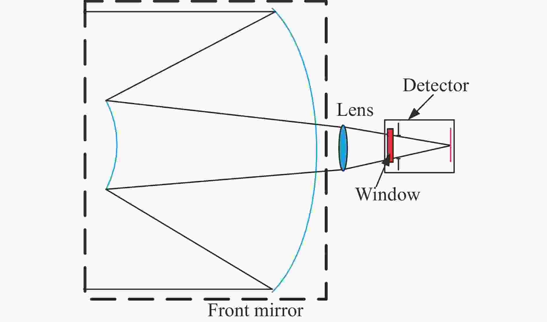
图 1 常温折反光学系统
Figure 1. Ordinary temperature optical system of refraction-reflection
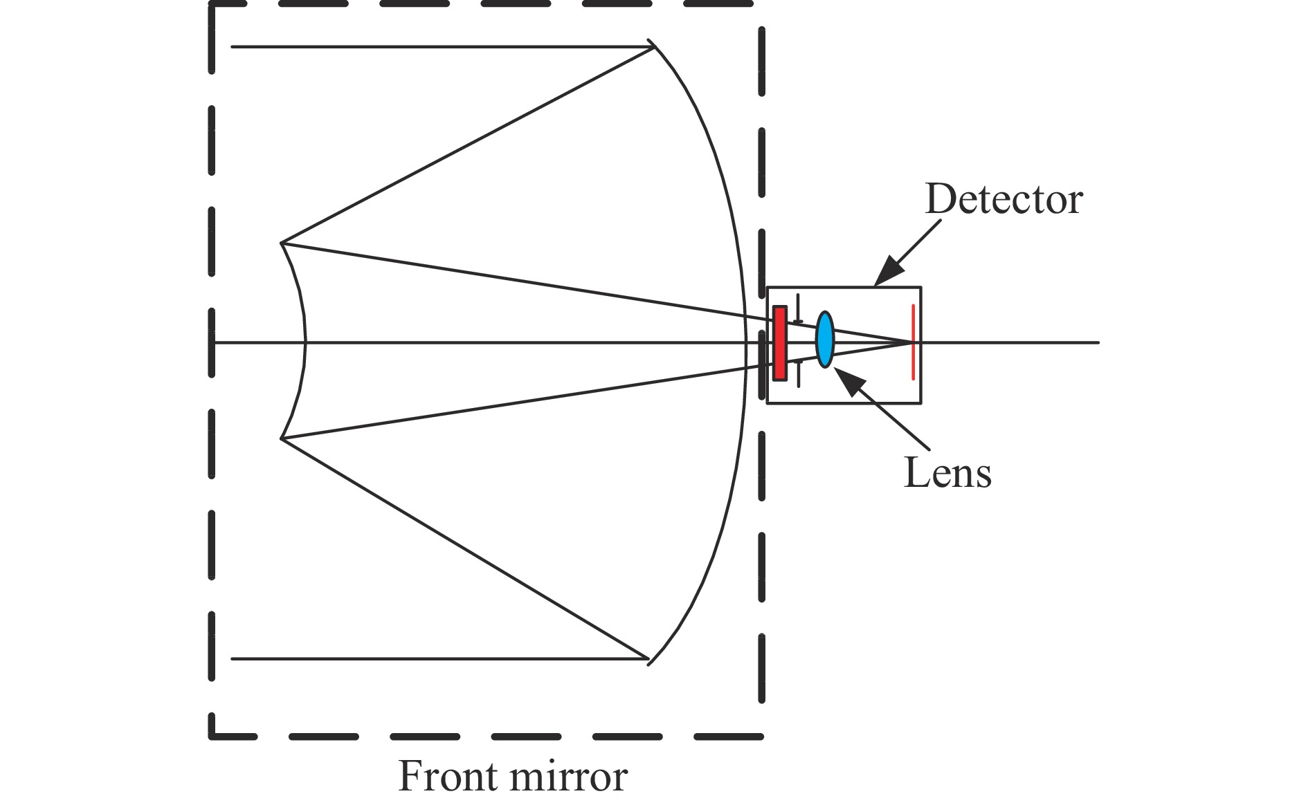
图 2 低温折反光学系统
Figure 2. Low temperature optical system of refraction-reflection
采用这种设计方式有几方面优点:
(1) 传统常温光学系统中透镜组是主要的自辐射源,将透镜组与芯片一起均匀制冷后,透镜组造成的自辐射理论上可以忽略,光学系统整体自辐射得到很大程度抑制;
(2) 比起给整个光学系统制冷而言,单独给透镜组制冷需要的制冷量少和制冷时间缩短,利于对制冷时间有需求的系统应用;
(3) 红外系统的能量接收主要受到前组光学系统口径决定,不会由于透镜组制冷而造成通光量衰减;
(4) 光学系统和探测器结构空间共用,封装到探测器杜瓦内部后,光路会缩短,有利于系统轻小型。
-
前一节通过光学系统局部制冷的方式实现光学系统自辐射抑制,系统等效背景辐射降低,灵敏度会提高,在此基础上研究多波段实现方式。
-
最简单的方式,是将单波段芯片换成双/多波段芯片,系统自然可以实现双波段或多波段能力,如图3所示,其中红外芯片是一个叠层双波段芯片。
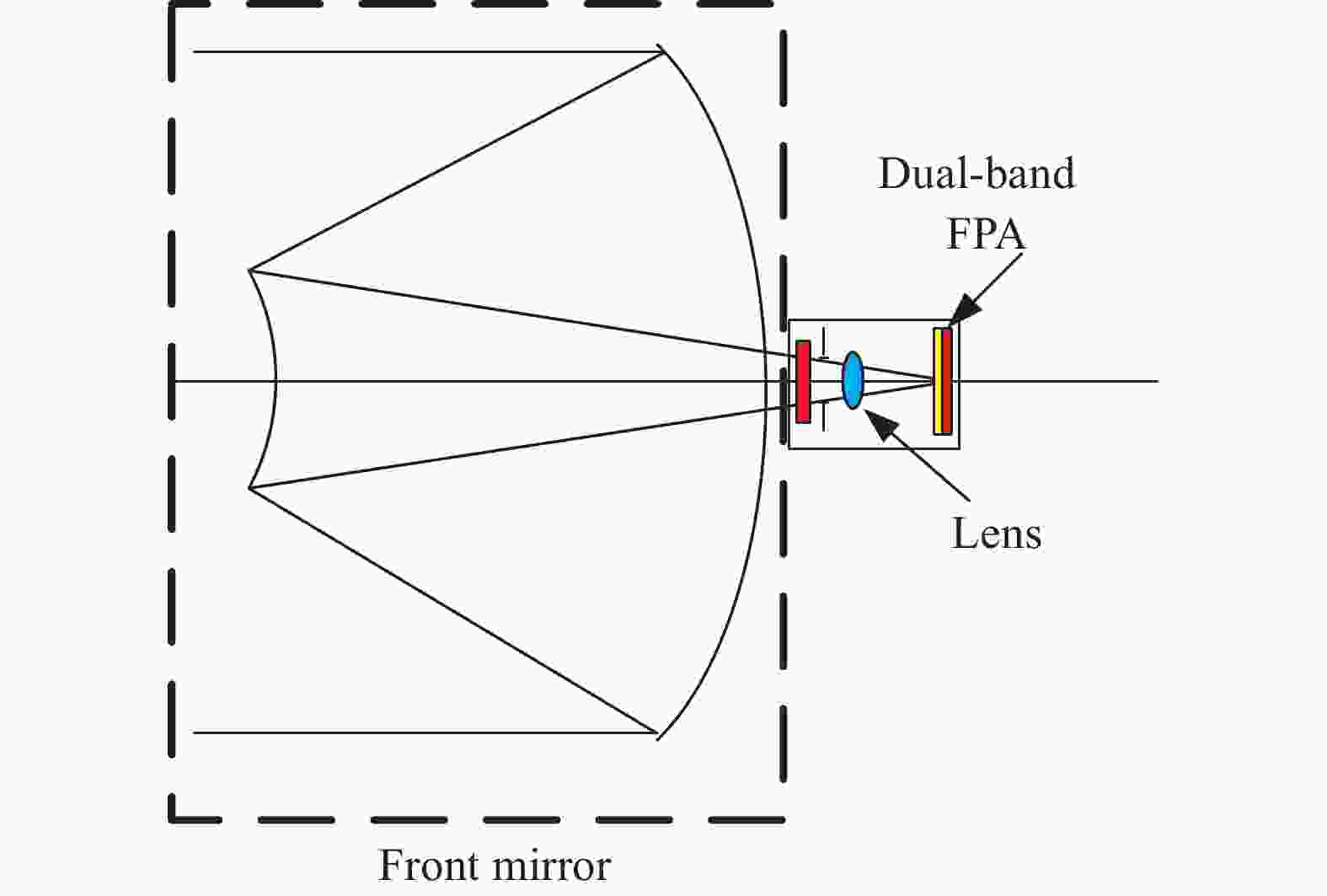
图 3 基于叠层双波段芯片的探测系统
Figure 3. Detection system based on dual-band FPA
-
文中重点研究的是在透镜组后面增加一个分光元件,并将分光元件和透镜组一起随芯片制冷,其中分光元件将光线分成两路,一路反射偏短波光线,光线在红外芯片2上完成光电转换;而另外一路实现透射偏长波光线,在红外芯片1上实现光电转换,至此,实现双波段能力,如图4所示。
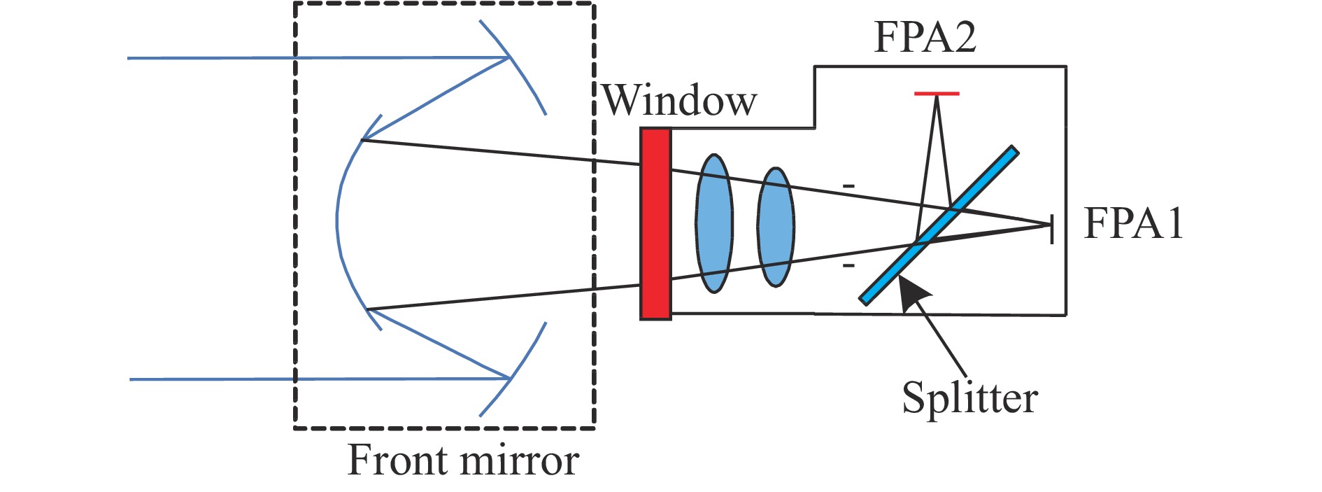
图 4 光学分光实现双波段探测系统
Figure 4. Dual-band detection system by optical splitter
该方案通过增加一路分光片就可以实现双波段能力,而且谱段可基于芯片或分光片任意编辑,理论上可以实现中/长,长/长以及长/甚长等任意波段组合;而且分光片也和透镜组一起制冷,背景辐射不会由于分光片增加而提高,而且当红外叠层芯片成熟后,将其中一个单波段芯片替换,可以扩展到三波段,甚至四波段等多波段能力。
尽管分光可以实现多波段能力,但是分光是在常温装配低温验证,如何保证常温下的装配精度满足低温下分光后的成像质量,是主要技术难点;同时分光技术面临的分光光学元件、低温冷屏等元件也需要制冷,造成分光系统的热质量较大,需要比传统系统更多的冷源。
-
为了能定量的评估出本技术的优势,这里将文中研究的探测技术与传统探测技术分别进行同条件分析及评估,分两项内容研究:(1)光学系统自辐射能力分析与评估;(2)灵敏度能力分析与评估。
-
光学系统自辐射能力分析与评估采用单波段方式就可以验证,因此,仿真时基于单波段完成杂光分析模型设计,其中,光学自辐射仿真软件采用的是通用的光学杂光分析软件Lighttools7.0。设定的基本参数和仿真分析结果如表1所示。
从上面仿真分析可以看出采用文中研究的低温折反光学系统是传统常温的折反系统的1/4,是同轴四反光学系统自辐射的1/2,自辐射抑制效果比较明显。
表 1 光学系统自辐射分析
Table 1. Self-radiation analysis of optical system
Parameter Wave band: 7.5-10.5 μm; Optical field of view: 2.5°×2.5°; f/#=2; Optical reflectivity: 99.2%;
Lens transmission: 98.5%; Metal absorptivity: 20%; Metal reflectivity: 80%Type Ordinary temperature optical system of refraction-reflection Coaxial four anti optical system Low temperature optical system of refraction-reflection Energy of self-radiation/W 2.6×10⁻⁵ 1.47×10⁻⁵ 6.5×10⁻⁶ Equivalent blackbody temperature/K 223 204 183 -
对于低背景探测系统而言,探测目标在成像像面上理论上是一个点,应该用系统灵敏度的等效噪声照度(NEFD)来分析评估。
其中,探测系统的灵敏度(NEFD)由时域灵敏度(NEFDt)和空域灵敏度(NEFDs)两部分组成,表示如下:
$$NEFD = {(NEFD_{\rm{t}}^2 + NEFD_{\rm{s}}^2)^{1/2}}$$ (1) 时域灵敏度(NEFDt)表示如下:
$$NEFD_{\rm{t}} = \frac{{4(f/\# ){{(\xi \alpha \beta \Delta f)}^{1/2}}}}{{ {\text{π}} {D_0}{\tau _0}{D^*}{K_1}{K_2}}}$$ (2) 式中:D0为光学系统口径;f/#为数值孔径参数;τ0为
光学透过率;ξ 为探测器填充率;K1为光学弥散系数;K2为电路损失系数;α和β分别为俯仰方向瞬时视场、瞬时视场;D*为归一化探测率。 空域灵敏度(NEFDs)表示如下:
$$NEFD_{\rm{s}} = \frac{U}{ {\text{π}} }\xi \alpha \beta {E_{\rm{b}}}$$ (3) 这里对三种状态情况进行比较分析:(1)常温折反分光双波段系统;(2)基于叠层芯片低温折反双波段系统;(3)低温折反分光双波段探测系统。其中,常温折反分光双波段系统,是一种国内比较常用的共口径双波段系统技术途径,光学镜片和分光片都在常温环境中,图5为常温折反分光双波段示意图。
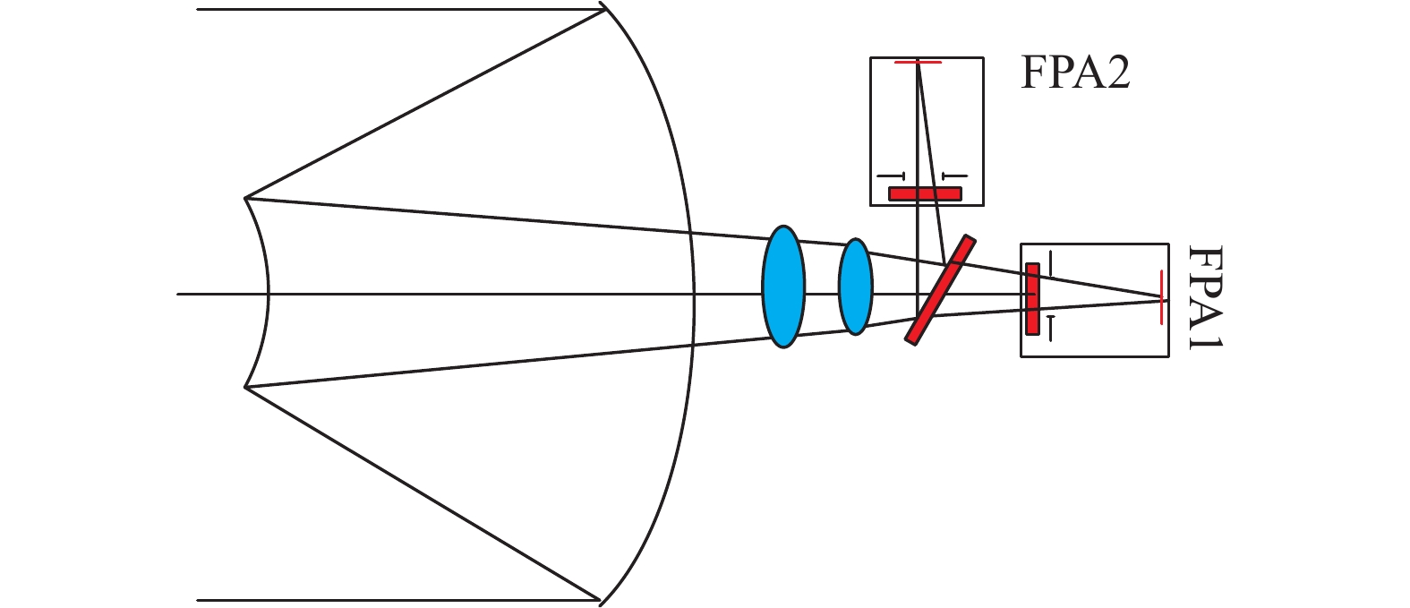
图 5 常温折反分光实现双波段系统
Figure 5. Dual-band detection system by optical splitter based on ordinary temperature refraction-reflection optical system
如前所述,低背景探测大部分以长波为主,这里分析也以长/长双波段探测系统进行比对分析,由于国内没有长/长叠层芯片,这里单波段芯片和叠层双波段芯片都以美国芯片能力为基础进行比较分析[3-5]。
首先,分析不同光学结构形式、不同探测器下的积分时间以及D*等参数进行理论推算,有些探测器指标根据国外资料推出。
(1) 积分时间理论计算
对于低背景探测系统而言,积分时间主要受到读出电路自身电荷存储能力、光电流以及器件自身暗电流决定的,具体如公式(4)和(5)所示:
$${e_{0{\text{光}}}} = \frac{{{Q_{\text{光}}}.{\tau _0}.{A_{\rm{d}}}.k}}{{4{{\left( {f/\# } \right)}^2}}}$$ (4) $${e_{\text{存储}}} = \left( {{e_{0{\text{光}}}} + {e_{0{\text{暗}}}}} \right) \times {t_{{\rm{int}}}}$$ (5) 式中:Q光为光学自辐射产生黑体辐射的光子流数;
${\tau _0}$ 为探测器的光电转换效率;Ad为探测器单位像元的面积;K 为探测器的像元填充率;f/#为系统参数;tint为系统探测积分时间;e0光为光学系统自辐射产生的光子流;e0暗为探测器自身暗电流水平;e存储为探测器电路电荷存储能力。而从国外资料可以看出长波暗电流一般都小于100 pA,基本可以忽略不计,影响探测积分时间长短主要受到光学系统自身热辐射引起的光电流影响。
因此,从国外文献上看,当光学系统达到183 K,单芯片积分时间可以达到6 ms,而如果用叠层芯片,理论上电容存储容量会被分割一半,积分时间变成3 ms;如果采用常温系统,如表1分析所示,光电流会增加4倍,单芯片积分时间理论上会变成1.5 ms;
(2) D*理论计算
美国的文献上一般用NEQ或NEI[3](噪声等效光子流数)来表征探测器能力,而国内用D*来表示,这俩之间的转换关系如公式(6)所示:
$${D^*} = \frac{{hc}}{{NEQ \times \lambda }}\sqrt {\frac{1}{{2{t_{{\rm{int}} }}{A_{\rm{d}}}}}} $$ (6) 式中:h为普朗克常数;λ为中心波长;c为光速。
通过公式(6)可以有效获得国外单波段探测器D*和叠层探测器D*,具体如表2所示。
表 2 D*分析
Table 2. D* analysis
Stacked dual FPA(183 K) Two FPA(183 K) NEQ(ph·cm2·s−1) D*(cm·Hz1/2·W−1) NEQ(ph·cm2·s−1) D*(cm·Hz1/2·W−1) Band 1: 4×10¹¹;
Band 2: 6×10¹¹Band 1: 4.2×10¹¹;
Band 2: 3×10¹¹Band 1: 1.22×10¹¹;
Band 2: 2.15×10¹¹Band 1: 8×10¹¹;
Band 2: 5×10¹¹当光学系统背景辐射提高,积分时间变短,系统的D*值会降低,具体见公式(7)所示:
$${D^*} = \frac{{\sqrt {({A_{\rm d}} \times 2\;1/{t_{{\mathop{\rm int}} }})} }}{{NEP}}$$ (7) 因此,当光子流提高4倍,积分时间降低4倍,D*值理论上降低至原来的1/2。
(3)系统灵敏度NEFD分析
根据上面的分析,可以获得系统的NEFD如表3所示。
表 3 三种不同双波段探测系统能力分析
Table 3. Ability analysis of three different dual-band detection systems
TYPE Ordinary temperature refraction-reflection dual-band detection system Dual-FPA detection system Low temperature refraction-reflection dual-band detection system Main parameter Band 1: 7-8.5 μm;
Band 2: 10-11.5 μm;
Optical field of view:2.5°×2.5°;
f/#=2;
Equivalent blackbody
temperature: 220 K;Band 1: 7-8.5 μm;
Band 2: 10-11.5 μm;
Optical field of view: 2.5°×2.5°;
f/#=2;
Equivalent blackbody
temperatur: 183 K;Band 1: 7-8.5 μm;
Band 2: 10-11.5 μm;
Optical field of view: 2.5°×2.5°;
f/#=2;
Equivalent blackbody
temperatur: 183 K;Theory parameter by calculation Int: 1.5 ms;
Band 1 D*: 4×10¹¹ (cm·Hz1/2·W−1);
Band 2 D*: 2.5×10¹¹ (cm·Hz1/2·W−1);Int: 3 ms;
Band 1 D*:4.2×10¹¹ (cm·Hz1/2·W−1);
Band 2 D*:3×10¹¹ (cm·Hz1/2·W−1);Int: 6 ms;
Band 1 D*: 8×10¹¹ (cm·Hz1/2·W−1);
Band 2 D*: 5×10¹¹ (cm·Hz1/2·W−1);NEFD(W/cm2) Band 1: 0.6×10⁻¹⁴ ;
Band 2: 0.85×10⁻¹⁴Band 1: 0.34×10⁻¹⁴;
Band 2: 0.6×10⁻¹⁴Band 1: 0.13×10⁻¹⁴;
Band 2: 0.26×10⁻¹⁴从表3可以看出:
(1) 相比常温折反分光系统,低温折反分光双波段系统由于提供较低等效背景,能获得高灵敏度(D*)和探测积分时间,从而提高系统灵敏度;
(2) 相比叠层芯片而言,由于低温折反系统单芯片有较高的填充率、电容存储能力以及较低暗电流,可以获得更高的灵敏度;
分析下来,低温折反分光系统可以充分发挥单芯片能力,也可以将辐射抑制下来,将每个多波段系统灵敏度做到与单波段系统的能力一致,具有很大的潜力和优势。
-
文中提出了一种折反光学结构形式光学局部制冷技术,理论分析了背景辐射降低至传统常温系统的1/4相比同类同轴四反结构形式而言也有明显优势,因此,在低背景探测条件下,该技术可以大幅提高系统灵敏度,由于光学探测器一体化设计实现空间共用,压缩光路,有助于降低系统体积尺寸;在此基础上,可以通过采用叠层芯片或光学分光方式实现双波段,也可以将叠层芯片和分光技术共用,可以拓展到多波段能力,该技术理论上可以满足全红外谱段应用;最后文中分别对该技术的光学系统自辐射效果及灵敏度与其他系统进行分析和比较,可以很明显看出:文中提出技术具有很明显的指标优势。
A novel technology on infrared multi-band low-background detection
-
摘要: 红外低背景探测技术主要应用在深空环境,系统灵敏度与自身背景辐射关系较大,如何有效抑制探测系统自身背景辐射一直是重点研究方向;识别一直是红外领域的研究热点,增加探测谱段是提高特征获取量的最有效方式。介绍了一种局部制冷分光的红外多波段探测技术,该技术采用探测器一体化设计思路,将折反结构光学系统局部集成到探测器内部随红外芯片一起制冷;再利用分光元件进行双路分光,实现双波段能力,如果结合叠层芯片可以有效拓展到多波段能力;通过光学自辐射仿真,比较不同光学结构形式下的自辐射结果,可以看出:该技术背景辐射降低至常温折反系统背景辐射1/4,理论灵敏度可以大幅度提高,该技术优势明显,潜力巨大。Abstract: Infrared low-background detection technology is mainly used in space environment, the sensitivity of detection system has a gret relationship with the background radiation of detection system. How to effectively suppress the background radiation of detection system has always been the important research direction. And recognition has been a research hotspot in infrared field, adding the detection spectrum is the most effective way to get the features of target. An infrared multi-band detection technology based on optical lens local refrigeration and optical spiltter was introduced. Firstly, adopting the idea of integrated design with optical system and detector, integrate local optical system into the infrared detector and refrigeration with infrared FPA, then dividing the two lights by optical spiltter, which achieved dual-band ability, if the dual-band FPA was used in the future, the system can have the multi-band ability. Comparing the results of self-radiation under different optical types by the simulation of optical self-radiation, it can be seen that the background radiation of this technology is reduced to 1/4 of the ordinary temperature optical system, the sensitivity has also been greatly improved. This technology has obvious advantages and great potential.
-
Key words:
- low-background detection /
- sensitivity /
- background radiation /
- infrared multi-band /
- refrigeration
-
图 5 常温折反分光实现双波段系统
Figure 5. Dual-band detection system by optical splitter based on ordinary temperature refraction-reflection optical system
表 1 光学系统自辐射分析
Table 1. Self-radiation analysis of optical system
Parameter Wave band: 7.5-10.5 μm; Optical field of view: 2.5°×2.5°; f/#=2; Optical reflectivity: 99.2%;
Lens transmission: 98.5%; Metal absorptivity: 20%; Metal reflectivity: 80%Type Ordinary temperature optical system of refraction-reflection Coaxial four anti optical system Low temperature optical system of refraction-reflection Energy of self-radiation/W 2.6×10⁻⁵ 1.47×10⁻⁵ 6.5×10⁻⁶ Equivalent blackbody temperature/K 223 204 183  下载: 导出CSV
表 2 D*分析
Table 2. D* analysis
Stacked dual FPA(183 K) Two FPA(183 K) NEQ(ph·cm2·s−1) D*(cm·Hz1/2·W−1) NEQ(ph·cm2·s−1) D*(cm·Hz1/2·W−1) Band 1: 4×10¹¹;
Band 2: 6×10¹¹Band 1: 4.2×10¹¹;
Band 2: 3×10¹¹Band 1: 1.22×10¹¹;
Band 2: 2.15×10¹¹Band 1: 8×10¹¹;
Band 2: 5×10¹¹
下载: 导出CSV
表 3 三种不同双波段探测系统能力分析
Table 3. Ability analysis of three different dual-band detection systems
TYPE Ordinary temperature refraction-reflection dual-band detection system Dual-FPA detection system Low temperature refraction-reflection dual-band detection system Main parameter Band 1: 7-8.5 μm;
Band 2: 10-11.5 μm;
Optical field of view:2.5°×2.5°;
f/#=2;
Equivalent blackbody
temperature: 220 K;Band 1: 7-8.5 μm;
Band 2: 10-11.5 μm;
Optical field of view: 2.5°×2.5°;
f/#=2;
Equivalent blackbody
temperatur: 183 K;Band 1: 7-8.5 μm;
Band 2: 10-11.5 μm;
Optical field of view: 2.5°×2.5°;
f/#=2;
Equivalent blackbody
temperatur: 183 K;Theory parameter by calculation Int: 1.5 ms;
Band 1 D*: 4×10¹¹ (cm·Hz1/2·W−1);
Band 2 D*: 2.5×10¹¹ (cm·Hz1/2·W−1);Int: 3 ms;
Band 1 D*:4.2×10¹¹ (cm·Hz1/2·W−1);
Band 2 D*:3×10¹¹ (cm·Hz1/2·W−1);Int: 6 ms;
Band 1 D*: 8×10¹¹ (cm·Hz1/2·W−1);
Band 2 D*: 5×10¹¹ (cm·Hz1/2·W−1);NEFD(W/cm2) Band 1: 0.6×10⁻¹⁴ ;
Band 2: 0.85×10⁻¹⁴Band 1: 0.34×10⁻¹⁴;
Band 2: 0.6×10⁻¹⁴Band 1: 0.13×10⁻¹⁴;
Band 2: 0.26×10⁻¹⁴
下载: 导出CSV
-
[1] 刁华飞, 李智. 天基光学空间监视指向策略研究[J]. 航天控制, 2011, 29(6): 39−43. Diao Huafei, Li Zhi. Study on the pointing strategy of space-based optical space surveillance [J]. Aerospace Control, 2011, 29(6): 39−43. (in Chinese) [2] 范晋祥. 美国动能拦截弹红外成像导引头的发展分析[J]. 红外与激光工程, 2009, 38(1): 1−6. doi: 10.3969/j.issn.1007-2276.2009.01.024 Fan Jinxiang. Development analysis of infrared imaging seeker of kinetic energy interceptor in the united states [J]. Infrared and Laser Engineering, 2009, 38(1): 1−6. (in Chinese) doi: 10.3969/j.issn.1007-2276.2009.01.024 [3] Herring J, Bollengier L, Madajian D, et al. Staring 256 × 256 LWIR focal plane array performanceof the Raytheon exoatmospheric kill vehicle[D].1998. [4] Smith E P G, Gallagher A M, Kostrzewa T J, et al. Large format HgCdTe focal plane arrays for dual-band long-wavelength infrared detection[C]//Optoelectronic and Microelectronic Matieral and Devices, 2010. [5] Smith E P G, Venzor G M, Gallagher A M, et al. Large-format HgCdTe dual-band long-wavelength Infrared Focal-Plane Arrays [J]. Electronic Materials, 2011, 40(8): 1630−1636. doi: 10.1007/s11664-011-1626-9 -

 点击查看大图

计量
- 文章访问数: 1121
- HTML全文浏览量: 595
- PDF下载量: 115
- 被引次数: 0


