


-
SiPM是具有光子数分辨能力的单光子探测器。它是由一系列工作于盖革模式的雪崩光电二极管(avalanche photodiode, APD)微单元并联而成,微单元间相互独立并与各自的淬灭电阻串联,所有微单元通过公共电极输出信号,信号大小正比于处于激发状态的微单元数目,即正比于探测到的光子数。与传统的光电倍增管(photomultiplier tube, PMT)相比,SiPM工作于非真空环境,因此不易损坏,SiPM体积小、不受磁场影响、功耗低、单光子分辨能力强,这些优势使得SiPM逐渐替代PMT成为具有广阔发展前景的单光子探测器,目前已广泛应用于天文物理、高能物理、激光雷达、核医学成像等方面[1-2]。
为了提升信噪比及线性响应范围,SiPM目前都是朝着低DCR、高增益(gain)、高PDE、高动态范围的方向改进,但不同应用对SiPM的特性关注点有所不同。在正电子发射断层扫描成像(positron emission tomography, PET)等高定时性能的应用中 ,低DCR有助于减少DCR带来的随机符合事件,提高定时性能[3]。另外,量能器对动态范围的要求促使SiPM朝着小微单元尺寸的方向发展[4]。目前,滨松发展了具有低DCR的S14160-3015 PS,在其推荐偏压下的典型DCR低于100 kHz/mm2[5]。FBK发展了具有大动态范围的UHD SiPM,微单元密度高达46190个/mm2[6]。
SiPM的淬灭电阻既可以在器件表面集成,也可以做在APD微单元下方,目前按淬灭电阻划分SiPM的结构主要有以下两种。表面多晶硅淬灭电阻型SiPM是最为普遍的结构[7],在器件表面集成分立的淬灭电阻条然后与APD单元相连,滨松、ON、FBK等均采用此结构,该结构由于淬灭电阻做在器件表面,限制了几何填充因子,具有一定的局限性。2010年,北京师范大学的NDL研制出利用P型硅外延层作淬灭电阻的N on P型SiPM[8],由于淬灭电阻不在器件表面,因此能够达到相对较大的几何填充因子,很好地兼顾了高PDE与大动态范围。
文中介绍了NDL 9 mm2 EQR SiPM的最新研究成果:微单元尺寸为15 μm的器件EQR15,通过优化器件设计和改进制作工艺,相较以往微单元尺寸为15 μm、有效面积为1 mm2的EQR SiPM[9],实现了DCR的明显降低同时保持较高的PDE,更有利于PET等核医学诊疗技术的应用;另外,新研制出的微单元尺寸为6 μm的器件EQR06,较以往EQR SiPM动态范围更大,同时保持了高PDE和较低的光学串扰率,特别适合应用于高能射线的探测。
-
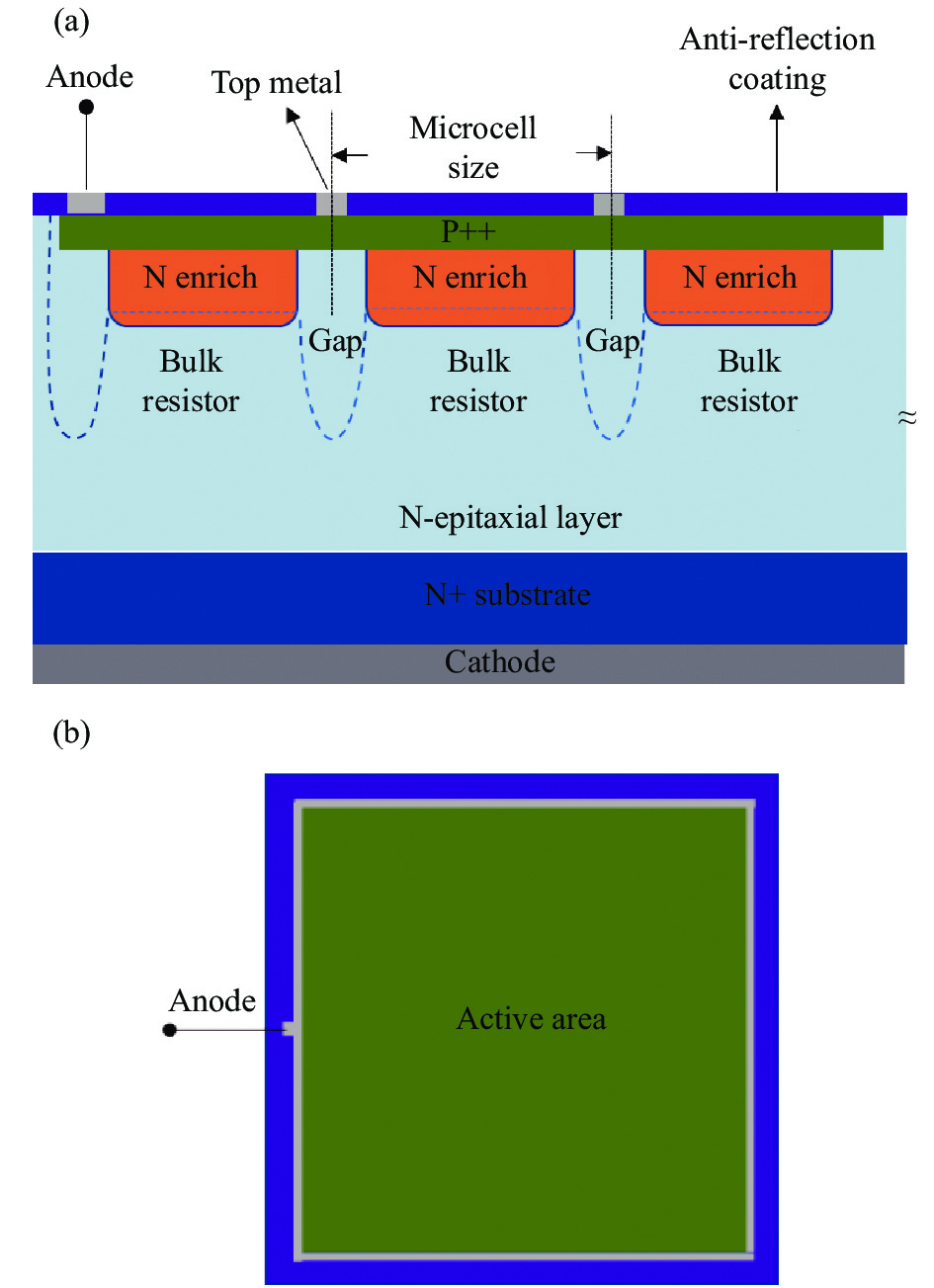
EQR SiPM的器件结构如图1所示,SiPM在反向偏置下工作,由少子触发雪崩事件,短波长光在硅中的吸收深度较浅,且因硅材料中电子的碰撞电离系数及迁移率均大于空穴,因此采用P on N的结构设计以增强器件对蓝紫光的探测灵敏度。器件表面重掺杂层P++与分区注入的N enrich区形成微单元PN结,结下方的N型外延层构成微单元淬灭电阻。由于外延层的掺杂浓度低于enrich区,微单元间Gap区的耗尽区深度大于微单元PN结的耗尽区深度,雪崩载流子将被限制在各自的微单元区域内,Gap区形成微单元间的电学隔离,最终信号通过公共电极输出。

图 1 P on N型EQR SiPM的结构示意图。(a)剖面结构;(b)平面结构
Figure 1. Structure diagram of P on N type EQR SiPM. (a) Profile structure; (b) Planer structure
EQR06与EQR15结构的不同之处在于:微单元尺寸分别为6 μm和15 μm。两类器件微单元尺寸不同,理论上特性的差别主要体现在直接串扰率(direct crosstalk probability, PDiCT)、PDE、增益。
EQR15-HE与EQR15-LE的唯一区别在于PN结的峰值电场强度。为了降低EQR15 SiPM的DCR,NDL优化器件设计和制作工艺,通过降低掺杂浓度降低PN结的峰值电场强度,有效抑制了场致隧穿引起的暗噪声成分,由EQR15- HE发展到EQR15-LE,从而降低了EQR15 SiPM的DCR,其他性能也获得优化。
-
SiPM主要表征I-V特性、DCR、PDiCT、PDE、单光子分辨谱、增益,以下特性无特殊说明外均为在20 ℃下的实验结果。
Keithley SMU对SiPM施加偏压,暗条件下测电流得 I-V曲线,确定器件击穿电压Vb及最大过偏压OVmax。暗条件下,Keithley SMU作为SiPM的偏置电源,其输出信号经过跨阻放大器(NDL AMP-40-1)输入示波器,Labview程序通过改变阈值测量计数率得到计数率随阈值的关系,由阈值为0.5 p.e.处的计数率得到DCR,由阈值为1.5 p.e.处的计数率与阈值为0.5 p.e.处的计数率之比得到PDiCT[10] ,其中1 p.e.代表SiPM中单个微单元发生雪崩时的输出信号幅度。
PDE是指一段时间内器件探测到的光子数与入射到器件表面的光子数之比。图2所示为PDE测试实验装置。图2(a)中采用函数发生器驱动LED产生脉冲光经窄带滤光片射入积分球,积分球出射光分别照射在已定标响应度的PIN和待测SiPM上, SiPM一端可通过加入衰减片以补偿PIN与SiPM的探测灵敏度差异,采集SiPM输出信号,根据泊松分布理论计算单次脉冲SiPM响应的平均光电子数μ[11],测量PIN的平均光电流IPIN,根据公式(1)得到单次脉冲入射至SiPM表面的光子数Nin:
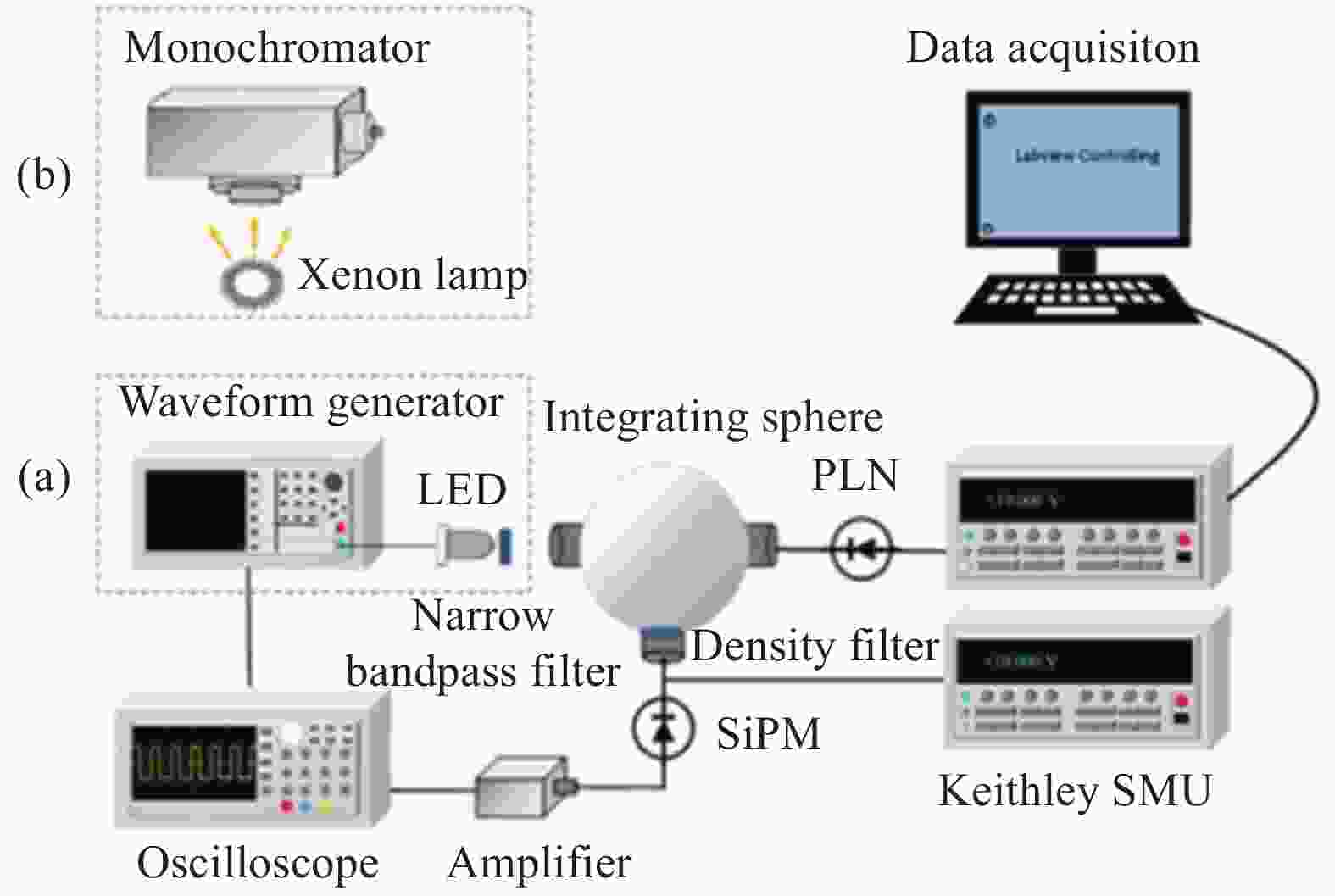
图 2 PDE测试实验装置示意图
Figure 2. Experimental setup diagram of PDE measurement
$$ {{{N}}_{{\rm{in}}}} = \dfrac{{{{{I}}_{{\rm{PIN}}}} \cdot {\rm{\lambda }} \cdot {{{P}}_{{\rm{SiPM}} - {\rm{PIN}}}}}}{{{{R}} \cdot {{h}} \cdot {{c}} \cdot {{f}}}}$$ (1) 式中:
$ \lambda $ 为光波长;R为PIN的响应度;f为入射光频率;h为普朗克常量;c为光速;${{P}}_{\mathrm{S}\mathrm{i}\mathrm{P}\mathrm{M}-\mathrm{P}\mathrm{I}\mathrm{N}}\mathrm{反}\mathrm{映}$ SiPM与PIN位置处入射光功率的比例因子。μ与Nin的比值为器件在该波长下的绝对PDE。图2(b)中采用氙灯作光源经单色仪射入积分球,采集SiPM的平均光响应计数率NL、平均暗计数率ND及PIN的平均光电流IPIN,由此可得PDE随波长的相对变化关系为[12]:
$$ {\rm{PDE}} = \dfrac{{\left( {{{{N}}_{\rm{L}}} - {{{N}}_{\rm{D}}}} \right) \cdot {{R}} \cdot {{h}} \cdot {{c}}}}{{{{{I}}_{{\rm{PIN}}}} \cdot {{\lambda }} \cdot {{{P}}_{{\rm{SiPM}} - {\rm{PIN}}}}}}$$ (2) 将PDE随波长的相对变化关系归一化到基于泊松分布理论的某一波长下的绝对PDE,以此扣除关联噪声的影响,修正后得到PDE随波长的变化关系[11]。
采用脉宽为100 ps的激光器光源,用示波器统计SiPM响应信号,由此获得脉冲面积直方图即为单光子分辨谱,通过相邻光子峰的平均面积差求得增益。
-
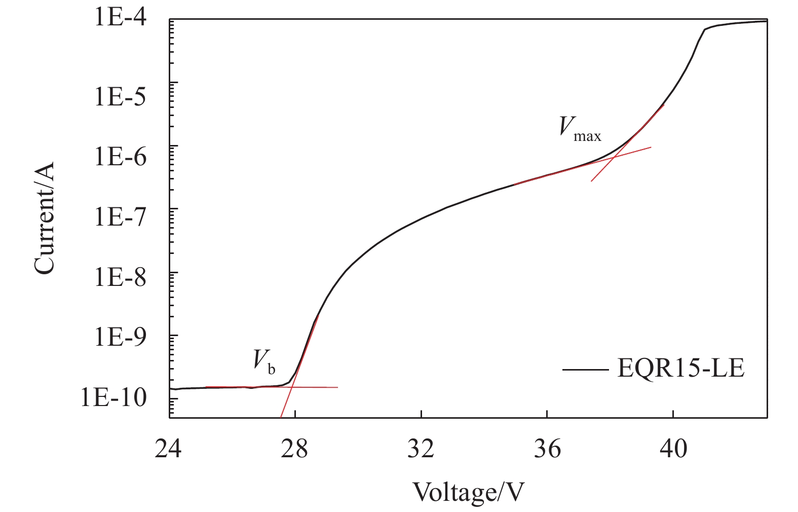
图3为以EQR15-LE为例的EQR SiPM的反向I-V曲线,由直线拟合求交点得到击穿电压Vb及最大过偏压OVmax (OVmax= Vmax−Vb)。EQR15-HE、EQR15-LE、EQR06的击穿电压分别为:20.2、28、24.5 V,最大过偏压分别为7、10、10 V。
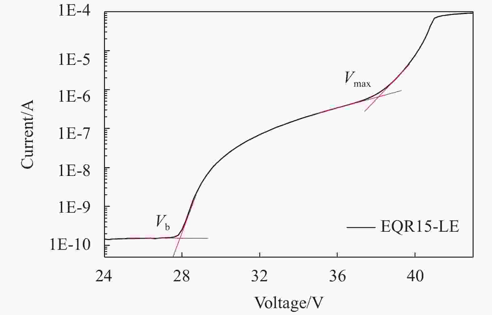
图 3 EQR SiPM的反向I-V曲线
Figure 3. Reverse I-V curve of EQR SiPM
温度升高,载流子的平均自由程变小,击穿时的临界电场增大,因此温度升高,Vb增大,SiPM偏置电压不变的情况下过偏压降低,使得SiPM的特性发生改变。选取−30~30 ℃为温度区间,测试了SiPM Vb随温度的变化关系,通过拟合求斜率得到Vb的温度系数,EQR15-HE、EQR15-LE、EQR06的温度系数分别为16、28、23 mV/℃。
-
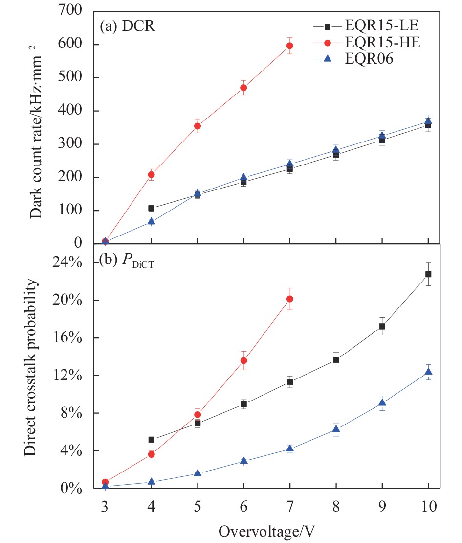
DCR是指单位时间内非待测粒子触发的雪崩脉冲计数,很大程度上反映了SiPM的噪声水平,按照DCR的产生机制分成初始DCR及延迟关联DCR。初始DCR主要来源于热激发、场致隧穿和中性区少子扩散[13]。禁带中的产生复合中心辅助载流子实现带间跃迁,此为热激发部分DCR的产生机制,主要由器件中的杂质密度及温度高低决定。当耗尽区内电场很强时,载流子可以直接隧穿实现带间跃迁,此为场致隧穿部分DCR的产生机制,主要由耗尽区内电场决定。中性区少子扩散部分DCR的大小则与耗尽区边界的载流子浓度梯度有关。
如图4(a)所示为DCR随过偏压变化的关系图,对于EQR15来说,从EQR15-HE~EQR15-LE,DCR随过偏压的斜率降低,过偏压OV=7 V时,DCR由596 kHz/mm2 (EQR15-HE)降低到226 kHz/mm2 (EQR15-LE) ,DCR得到显著降低。对于EQR06,综合考虑器件整体信噪比,调制内部场强使得其在过偏压为7 V时,DCR为240 kHz/mm2。

图 4 DCR及PDiCT随过偏压的关系
Figure 4. DCR and PDiCT as a function of overvoltage
PDiCT反映了器件的光学串扰概率。如图4(b)所示为PDiCT随过偏压变化的关系图,EQR15-LE与EQR15-HE的PDiCT随过偏压的变化趋势略有不同,EQR15-LE在过偏压为7 V时,PDiCT为11%。EQR06相比EQR15器件的微单元面积小增益低,因此单次雪崩事件产生的平均串话光子少, DCR几乎相同的情况下,PDiCT低,过偏压为7 V时,其PDiCT仅为4%。
-
如图5所示,首先测试LED由不同频率脉冲驱动下PIN与SiPM的响应光电流,以此确定探测器保持线性响应的实验条件。另外,为了防止由上一个LED周期内引发的SiPM的后脉冲被误认为下一个LED周期的光响应事件[12],驱动频率的选取既要保证两器件的线性响应,同时LED的脉冲驱动周期应大于SiPM的后脉冲时间常数。综合考虑,文中实验选取驱动LED的脉冲频率为1 MHz,脉宽为16 ns。

图 5 固定驱动电压及脉宽,PIN及SiPM的光电流随LED驱动频率的关系(SiPM以EQR15-LE @4 V为例)
Figure 5. Fix driving voltage and pulse width, photocurrent of PIN and SiPM as a function of LED driving frequency, with EQR15-LE @4 V as an example
如图6所示是EQR SiPM在420 nm处基于泊松理论的PDE实验结果。EQR15-LE的PDE稍低于EQR15-HE,过偏压为7 V时,PDE为46%。由于EQR06的几何填充因子比EQR15小,PDE相对较低,过偏压为7 V时,PDE为28%。
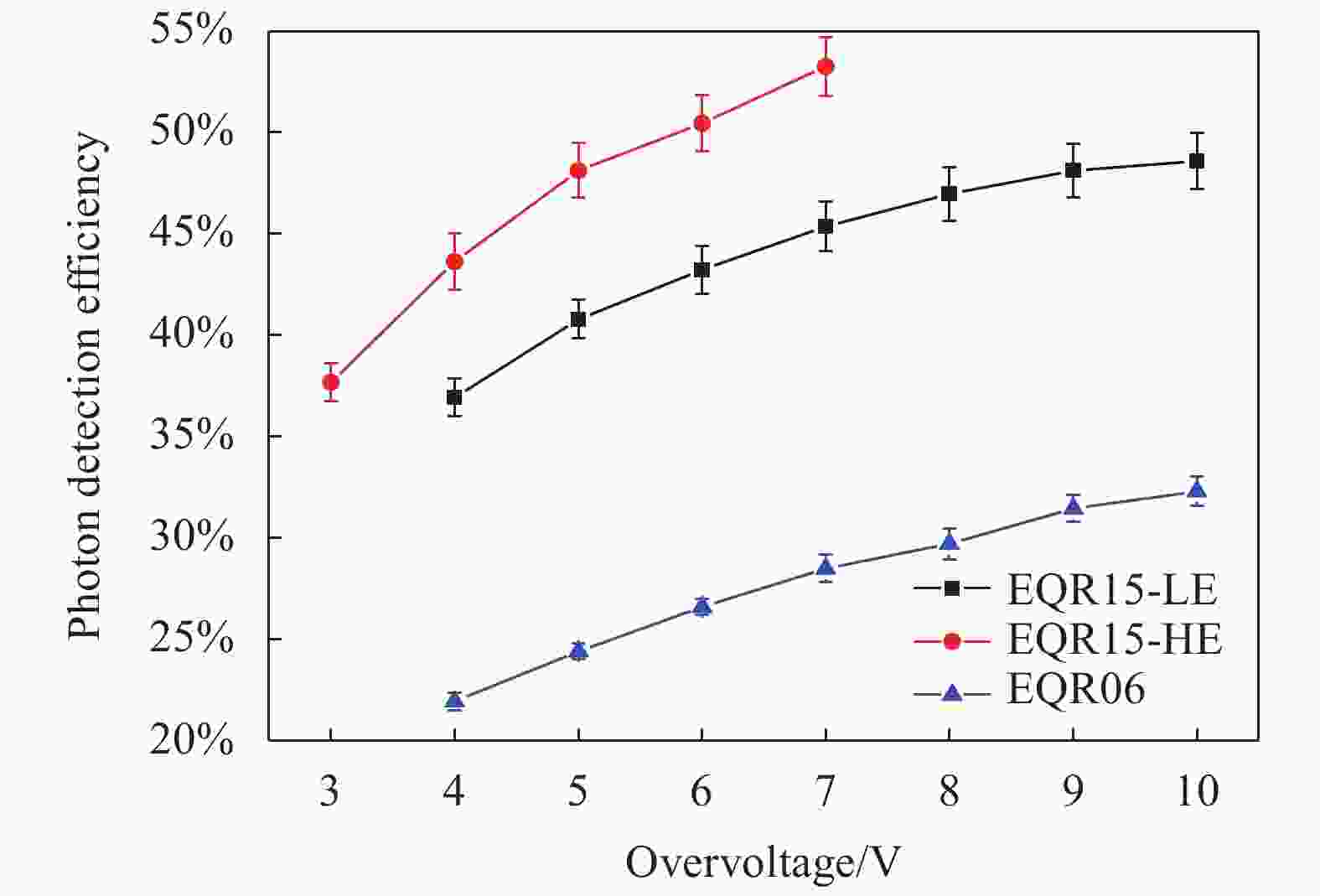
图 6 420 nm处,PDE与过偏压的关系
Figure 6. PDE as a function of overvoltage at 420 nm
随着偏压的增大,PDE逐渐趋于饱和,但DCR仍线性增加,图7示出了器件在各自最佳推荐过偏压下,PDE随波长的变化关系。如1.2节所述方式,图中曲线为PDE随波长的相对变化关系归一化到420 nm的绝对PDE得到的PDE随波长的变化关系,另外,图中的散点为器件在420、532 nm处利用泊松统计理论测得的绝对PDE。可看出利用此方式得到的PDE随波长变化关系在532 nm的PDE与在该波长下采用泊松统计得到的绝对PDE基本一致。峰值波长处,EQR15-LE的PDE稍低于EQR15-HE,但是450 nm以上波段PDE差异很小。在7 V过偏压下,EQR06峰值波长处PDE为28%。

图 7 PDE随波长的变化关系
Figure 7. PDE as a function of wavelength
-
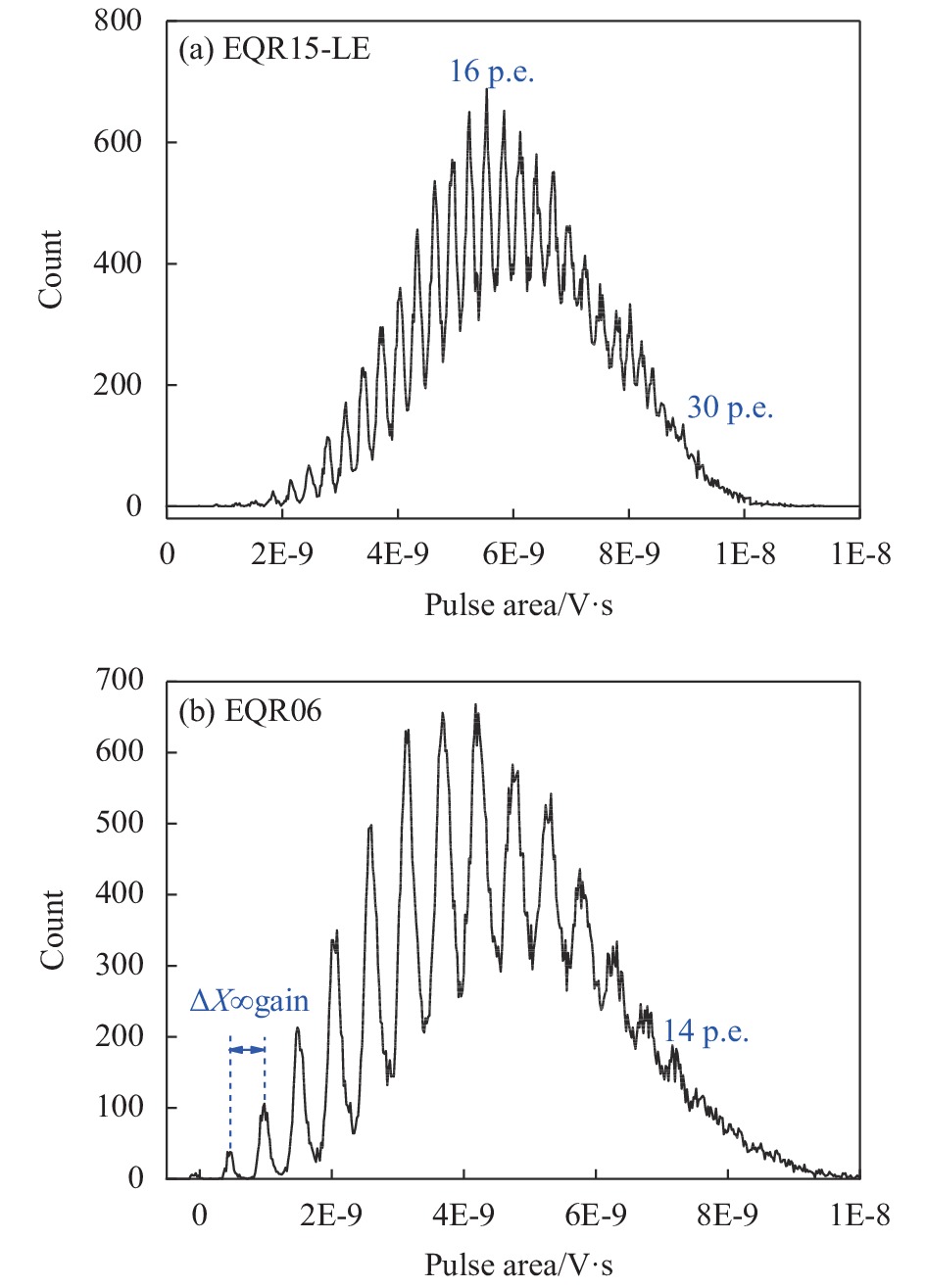
单光子分辨谱中第一个峰是指系统噪声贡献的基线峰,第n个峰代表器件探测到n-1个光子。SiPM的输出信号正比于探测到的粒子数,理想情况下,器件发生一次雪崩倍增释放的电荷量是固定的,因此相邻光子峰之间的差值为定值。事实上,受增益的统计涨落及后脉冲等延迟关联噪声的影响,每个峰都有一定的半高宽,对于单光子谱而言,峰谷比越好说明器件的信噪比越好,光子数分辨能力越强。如图8所示,在83% OVmax处,EQR15-LE能够分辨30个光子,在80%,OVmax处EQR06能够分辨14个光子。

图 8 脉冲面积直方图。(a) EQR15-LE @83%OVmax;(b) EQR06 series@80%OVmax
Figure 8. Histogram of pulse area. (a) EQR15-LE @83%OVmax;(b) EQR06 series@80%OVmax
增益是指SiPM的一个微单元发生一次雪崩释放的电子空穴对数,增益越大信号幅值越大,器件的信噪比越好。单光子分辨谱中相邻峰间距正比于增益,在不同过偏压下采集单光子分辨谱可得到增益随过偏压的变化。如图9所示为增益随过偏压的关系图,与EQR15-HE相比,EQR15-LE增益随过偏压的斜率降低,过偏压为7 V时,EQR15-LE的增益为3.5×10⁵。由于EQR06器件微单元尺寸相对较小,微单元等效电容低,因此EQR06的增益较低,过偏压为7 V时增益为7×10⁴。
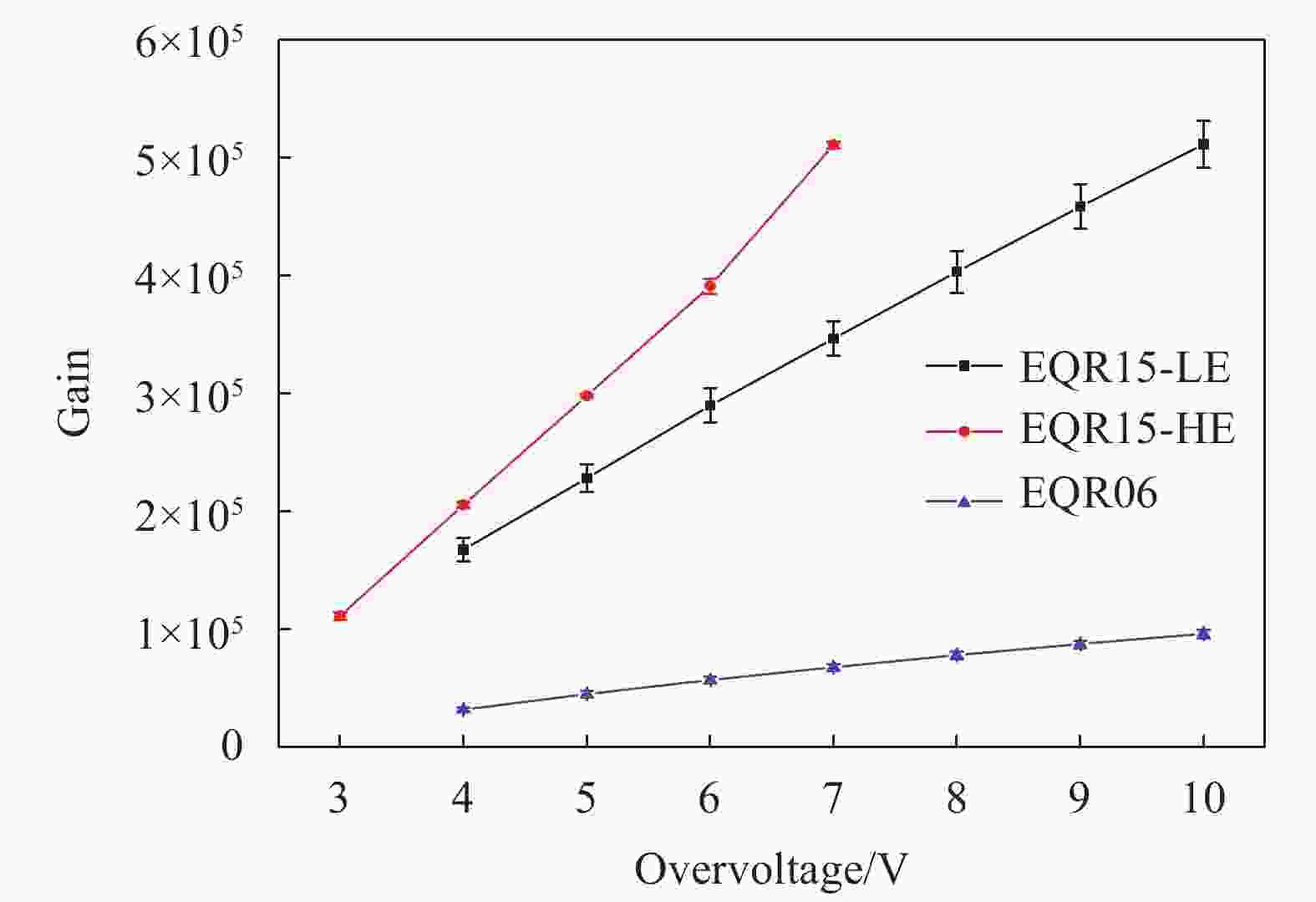
图 9 增益随过偏压的变化关系
Figure 9. Gain as a function of overvoltage
-
从EQR15-HE~EQR15-LE,通过工艺和设计优化,器件特性取得一定改进:
(1)场致隧穿部分的DCR正比于器件内部电场强度,器件内部电场降低使得场致隧穿部分的DCR降低,因此,DCR随电场的斜率降低,即DCR随过偏压的斜率降低。
(2)电场强度的降低导致耗尽区宽度增大,使得SiPM微单元的等效电容减小,而增益正比于微单元等效电容及过偏压,因此与EQR15-HE相比,EQR15-LE增益随过偏压的斜率降低。两者温度系数的不同来源于耗尽区宽度的差异,耗尽区宽度越大温度系数越高[14],EQR15-LE具有更高的温度系数。每105个穿过高场区的载流子平均会产生3个串扰光子[15],这体现在对于单次雪崩事件而言,增益越高产生的串扰光子越多。因此,EQR15-HE与EQR15-LE增益及DCR随过偏压的变化趋势不同进而导致PDiCT的不同。
(3) PDE的大小由几何填充因子、量子效率、盖革效率决定。碰撞电离系数与电场呈指数关系且正相关[15],器件内部电场降低导致电子空穴的碰撞电离系数减小进而盖革效率降低,影响PDE,这体现在短波长处PDE的降低。与此同时,尽管盖革效率存在一定程度的降低,但PN结峰值电场降低使得耗尽区展宽,更深吸收长度的长波长光子量子效率反而提升,因此,长波长处PDE改变很小。
-
表1为NDL EQR15-LE与滨松同类型S14160-3015 PS[5]的主要参数,两类器件具有相同的有效面积及微单元尺寸。两器件的动态范围近似一样,EQR SiPM的器件结构使得其几何填充因子更高,因而器件在各自的推荐偏压下(Vop),EQR SiPM有更优PDE。EQR SiPM与MPPC的增益相近,只是其DCR及PDiCT不及MPPC。EQR SiPM的结电容远小于MPPC,意味其输出信号脉宽更窄,在高计数率应用中,脉冲堆叠现象的影响会比MPPC小。
表 1 NDL与滨松SiPM的主要特性参数对比
Table 1. Main characteristic parameters comparison between NDL and HAMAMATSU SiPM
Research institute HAMAMATSU NDL Series S14160-3015 PS EQR15 11-3030 D Active area/mm2 3.0×3.0 3.0×3.0 Microcell size/μm 15 15 Microcell number 39984 40000 Breakdown voltage (Vb)/V 38±3 28±0.2 Recommended operating voltage (Vop)/V Vb+4 Vb+7 Photon detection efficiency (PDE) @Vop 32% @460 nm 46% @410 nm Gain @Vop 3.6×10⁵ 3.5×10⁵ Dark count rate (DCR) @Vop Typical: 700 kHz Typical: 2 000 kHz Crosstalk probability @Vop <1% 11% Terminal capacitance/pF 530 48 FBK于2018年报道出微单元尺寸为5 μm、微单元密度高达46190个/mm2的超高密度UHD SiPM[6],在接近6 V的工作条件下,增益约为1.8×10⁵,在545 nm处,PDE约为12%,但DCR高于800 kHz/mm2。与其相比,EQR06 SiPM微单元密度低于UHD SiPM,在推荐过偏压处,增益为7×10⁴,峰值波长处PDE为28%,DCR约为240 kHz/mm2,整体特性优于FBK 微单元尺寸为5 μm的UHD SiPM。
-
NDL最新的研究成果包括EQR15 3030 D的改进及EQR06 3030 D新系列的研制。EQR15系列通过优化设计和工艺改进降低PN结的峰值电场强度, DCR得到显著降低,环境温度为20 ℃、过偏压为7 V时,DCR的典型值为226 kHz/mm2、峰值PDE为46%。另外,研制出的超高微单元数目的EQR06 3030 D系列SiPM,兼顾了高PDE与大动态范围,适合高能物理方面的应用。
Recent research progress of silicon photomultiplier with epitaxial quenching resistor
-
摘要: 北京师范大学新器件实验室(NDL)一直致力于研制结构紧凑、工艺相对简单的外延电阻淬灭型硅光电倍增器(silicon photomultiplier with epitaxial quenching resistor, EQR SiPM)。近期为了满足硅光电倍增器(silicon photomultiplier, SiPM)在核医学成像方面的需要,NDL通过优化器件设计和制作工艺,成功研制出微单元尺寸为15 μm、有效面积为9 mm2的EQR SiPM。相较以往同类型器件,实现了器件暗计数率(dark count rate, DCR)的进一步降低同时保持了较高的光子探测效率(photon detection efficiency, PDE),在环境温度为20 ℃、过偏压为7 V时,DCR的典型值为226 kHz/mm2、峰值PDE为46%。另外,为了进一步提升EQR SiPM的动态范围,NDL还研制出微单元尺寸为6 μm、有效面积为9 mm2、微单元数目为244720的EQR SiPM,在环境温度为20 ℃、过偏压为7 V时,DCR的典型值为240 kHz/mm2、峰值PDE为28%,其较大的动态范围特别适合高能宇宙射线的测量、强子量能器等应用。Abstract: The Novel Device Laboratory (NDL) of Beijing Normal University has been developing a silicon photomultiplier with an epitaxial quenching resistor (EQR SiPM), which has a compact structure and a relatively simple fabrication process. Recently, to meet the requirements of nuclear medicine imaging, NDL has successfully developed an EQR SiPM with a microcell size of 15 μm and an active area of 9 mm2 by optimizing the device structure and fabrication technology. Compared to previous devices of the same type, the dark count rate (DCR) of the EQR SiPM is further reduced while still maintaining high photon detection efficiency (PDE). At an ambient temperature of 20 ℃ and an operating overvoltage of 7 V, the typical DCR is 226 kHz/mm2, and the peak PDE is 46%. In addition, to further increase the dynamic range of the EQR SiPM, NDL has developed an EQR SiPM with a microcell size of 6 μm, an active area of 9 mm2 and a microcell number of 244720. At an ambient temperature of 20 ℃ and an operating overvoltage of 7 V, the typical DCR is 240 kHz/mm2, and the peak PDE is 28%. It has large dynamic range that is very suitable for the measurement of high-energy cosmic rays and other applications in hadron calorimeters.
-
图 1 P on N型EQR SiPM的结构示意图。(a)剖面结构;(b)平面结构
Figure 1. Structure diagram of P on N type EQR SiPM. (a) Profile structure; (b) Planer structure
图 5 固定驱动电压及脉宽,PIN及SiPM的光电流随LED驱动频率的关系(SiPM以EQR15-LE @4 V为例)
Figure 5. Fix driving voltage and pulse width, photocurrent of PIN and SiPM as a function of LED driving frequency, with EQR15-LE @4 V as an example
图 8 脉冲面积直方图。(a) EQR15-LE @83%OVmax;(b) EQR06 series@80%OVmax
Figure 8. Histogram of pulse area. (a) EQR15-LE @83%OVmax;(b) EQR06 series@80%OVmax
表 1 NDL与滨松SiPM的主要特性参数对比
Table 1. Main characteristic parameters comparison between NDL and HAMAMATSU SiPM
Research institute HAMAMATSU NDL Series S14160-3015 PS EQR15 11-3030 D Active area/mm2 3.0×3.0 3.0×3.0 Microcell size/μm 15 15 Microcell number 39984 40000 Breakdown voltage (Vb)/V 38±3 28±0.2 Recommended operating voltage (Vop)/V Vb+4 Vb+7 Photon detection efficiency (PDE) @Vop 32% @460 nm 46% @410 nm Gain @Vop 3.6×10⁵ 3.5×10⁵ Dark count rate (DCR) @Vop Typical: 700 kHz Typical: 2 000 kHz Crosstalk probability @Vop <1% 11% Terminal capacitance/pF 530 48  下载: 导出CSV
-
[1] Nagai A, Alispach C, Volpe D D, et al. SiPM behaviour under continuous light [J]. Journal of Instrumentation, 2019, 14(12): P12016. doi: 10.1088/1748-0221/14/12/P12016 [2] Gundacker S, Heering A. The silicon photomultiplier: fundamentals and applications of a modern solid-state photon detector [J]. Physics in Medicine & Biology, 2020, 65(17): 17TR01. [3] Gola A, Acerbi F, Capasso M, et al. NUV-sensitive silicon photomultiplier technologies developed at fondazione bruno kessler [J]. Sensors, 2019, 19(2): 308. doi: 10.3390/s19020308 [4] Simon F. Silicon photomultipliers in particle and nuclear physics [J]. Nuclear Instruments and Methods in Physics Research Section A: Accelerators, Spectrometers, Detectors and Associated Equipment, 2019, 926: 85-100. [5] Hamamatsu. S14160-3015PS: Low breakdown voltage, wide dynamic range type MPPC with small pixels[EB/OL]. [2021-09-12]. https://www.hamamatsu.com/jp/en/product/optical-sensors-/mppc/mppc_mppc-array/S14160-3015PS.html [6] Acerbi F, Gola A, Regazzoni V, et al. High efficiency, ultra-high-density silicon photomultipliers [J]. IEEE Journal of Selected Topics in Quantum Electronics, 2018, 24(2): 1-8. [7] Acerbi F, Paternoster G, Capasso M, et al. Silicon photomultipliers: technology optimizations for ultraviolet, visible and near-infrared range [J]. Instruments, 2019, 3(1): 15. doi: 10.3390/instruments3010015 [8] Zhang G Q, Hu X B, Hu C Z, et al. Demonstration of a silicon photomultiplier with bulk integrated quenching resistors on epitaxial silicon [J]. Nuclear Instruments and Methods in Physics Research Section A: Accelerators, Spectrometers, Detectors and Associated Equipment, 2010, 621(1-3): 116-120. doi: 10.1016/j.nima.2010.04.040 [9] 刘红敏, 龙金燕, 代雷, 等. 大动态范围外延电阻淬灭型硅光电倍增器[J]. 光学精密工程, 2020, 28(3): 535-541. doi: 10.3788/OPE.20202803.0535 Liu Hongmin, Long Jinyan, Dai Lei, et al. Research progress of large dynamic range silicon photomultiplier with epitaxial quenching resistor [J]. Optics and Precision Engineering, 2020, 28(3): 535-541. (in Chinese) doi: 10.3788/OPE.20202803.0535 [10] Nagai A, Alispach C, Barbano A, et al. Characterization of a large area silicon photomultiplier [J]. Nuclear Instruments and Methods in Physics Research Section A: Accelerators, Spectrometers, Detectors and Associated Equipment, 2019, 948: 162796. doi: 10.1016/j.nima.2019.162796 [11] Eckert P, Schultz-Coulon H C, Shen W, et al. Characterisation studies of silicon photomultipliers [J]. Nuclear Inst & Methods in Physics Research A, 2010, 620(2): 217-226. [12] Zappalà G, Acerbi F, Ferri A, et al. Set-up and methods for SiPM Photo-Detection Efficiency measurements [J]. Journal of Instrumentation, 2016, 11(8): P08014. doi: 10.1088/1748-0221/11/08/P08014 [13] Serra N, Ferri A, Gola A, et al. Characterization of new FBK SiPM technology for visible light detection [J]. Journal of Instrumentation, 2013, 8(3): P03019. doi: 10.1088/1748-0221/8/03/P03019 [14] Piemonte C, Gola A. Overview on the main parameters and technology of modern Silicon Photomultipliers [J]. Nuclear Instruments and Methods in Physics Research Section A: Accelerators, Spectrometers, Detectors and Associated Equipment, 2019, 926: 2-15. doi: 10.1016/j.nima.2018.11.119 [15] Fa A, Sgb C. Understanding and simulating SiPMs [J]. Nuclear Instruments and Methods in Physics Research Section A: Accelerators, Spectrometers, Detectors and Associated Equipment, 2019, 926: 16-35. -

 点击查看大图
计量
- 文章访问数: 220
- HTML全文浏览量: 69
- PDF下载量: 45
- 被引次数: 0


