


-
红外光电探测器在航空航天、目标侦探、卫星遥感和红外制导等领域有着广泛的应用,并逐步向着高集成度、高性能、多维度探测和低成本的方向发展,对于响应速度、探测灵敏度、响应时间和器件的体积、质量和成本等指标提出了更高的要求。
在增强探测器性能的各种技术中,微纳结构能有效提高等效光程,突破传统体材料的吸收极限,提高光电器件的量子效率,为高性能红外探测器的研究提供了全新的技术手段[1-4]。近年来,研究人员通过在探测器表面集成各类不同类型和功能的微纳结构,在拓展探测器响应波段、提高探测率、响应速度,以及实现探测器的小型化和集成化,降低红外探测器的尺寸、质量、功耗和价格上开展了大量研究工作[5-8],取得了积极有效的进展。利用微纳结构引入高效光耦合和亚波长光场局域效果,结合传统半导体器件的能级优化等调控方式实现探测器综合性能的提升,已成为目前红外探测器领域较为活跃和具有良好前景的研究方向。
在该背景下,文中综述了近年来集成微纳结构的红外光电探测器的最新研究进展。首先,介绍了不同类型的微纳结构增强红外探测器性能的基本原理,描述了介质型、表面金属型、三维等离子腔型三种不同微纳结构各自的特点,然后分别针对上述微纳结构在红外探测器上的研究现状和进展进行阐述,最后对该领域的未来发展和应用前景作出展望。
-
近年来,随着外延生长技术、单晶衬底制备技术和探测器制作工艺的不断成熟,红外探测器的性能得到了显著的提升,器件的非本征暗电流已得到了很好的抑制。要进一步提高红外探测器的性能,就需要在不增加或降低本征吸收层厚度的情况下提高器件对入射光的吸收率,并抑制与器件体积成正比的本征暗电流。
人工微纳结构设计与加工技术的进步为克服上述问题提供了有效的解决思路。微纳结构是指周期性的结构尺寸远小于或接近入射波长的特殊结构,在与光的相互作用过程中展现出许多独特的性质,提升了人们对电磁波的调控能力。由于周期调制导致的能带结构和局域光场,微纳结构可以操纵入射光子的行为和光生电子的输运特性,带来独特的光电响应。在红外探测器领域,利用微纳结构提高光子的耦合效率和吸收率,保持器件光学响应的同时降低器件吸收层的厚度和体积,从而降低了器件的暗电流,提高了器件探测率。
目前,在红外探测器研究中使用的微纳结构主要包括:介质型微纳结构、表面金属型微纳结构和三维等离子体腔型微纳结构等。介质型微纳结构是指直接在半导体器件的正面或背面进行微纳加工,形成周期性孔状或柱状结构调控入射光场,使光在微纳结构内多次反射和散射,通过增加光的传播路径来提升吸收率[9]。表面金属型微纳结构是通过在器件表面额外集成一层具有特定形貌的周期性金属微纳图形,在谐振波长处激发表面等离激元,提高光场密度,实现特定波长光的吸收增强[10]。三维等离子腔体结构则是一种三明治复合结构,在表面金属结构的基础上增加了中间的介质吸收层和底部的金属反射层,形成一种三维的谐振腔结构。上层的微纳金属结构与底部的反射层会在厚度较小的中间吸收层产生近场耦合效应,从而入射光通过后会在吸收层中产生强烈的局域增强现象[11]。通过调节微纳金属结构的形貌和吸收层的厚度,能够有效影响吸收层中电磁共振的频率和振幅。
上述微结构对红外探测器性能的增强首先体现在对特定入射光谱或宽光谱段的减反效果上。由于材料表面微纳结构组成界面的等效折射率低于材料本身,更易于与空气界面实现折射率匹配,最大限度降低入射光的反射率。如采用圆锥、漏斗、金字塔型等渐变型几何形貌的微纳结构,可使等效折射率具有连续的梯度渐变特性,从而在较宽的光谱范围和入射角度内降低界面的反射率。其次,微纳结构的增强作用体现在光吸收率(即光响应)的提升上,对薄层吸收材料尤为明显,峰值处光吸收率能超过传统材料的Yablonovitch吸收增强上限[12-13]。
这些微纳结构用于增强探测器光响应的作用机理和表现形式有所不同。介质型微纳结构通过导模谐振效应,使纵向传播的入射光变为横向传播模式,增加入射光在器件吸收层中的有效光程,从而提高了光吸收率;表面金属微纳结构主要通过激发金属-吸收层界面处的表面等离子体共振,提高吸收层的光场密度,增加了光吸收率;而三维等离子体腔结构则是通过局域等离子体共振,使谐振波长处的入射光局域在吸收层区域得到增强,进而可达到或超过传统材料的吸收极限。
探测器光吸收率的大幅提高意味着可以使用更薄的吸收层材料,而微纳结构本身也可以有效减小器件光敏单元的体积,这使得器件与材料体积相关的本征暗电流明显减小,从而进一步提高红外探测器的探测率和综合性能。
-
在传统的半导体探测器吸收层中加工出具有亚波长特征尺寸的微纳结构能有效增加材料的等效吸收光程,提高光敏源的光吸收率,同时降低本征暗电流,使器件的性能得到显著提升。目前,研究人员对介质型微纳结构在锗、硅、碲镉汞、III-V族半导体等探测器中的设计、加工和集成开展了系统研究[14-16]。
硅基探测器在制作成本和工艺兼容性上具有很大的优势,但是较低的近红外吸收率限制了它的应用。研究人员通过在探测器上集成波长响应较长的半导体材料和具有光捕获功能的微纳结构[17-18],在共振波长处产生局域增强的光场,提高了探测器对特定波段的光响应,拓展了探测器的应用场景。加州大学戴维斯分校的Cansizoglu等人提出了一种表面照明的高速锗硅光电二极管[19],结构示意图与量子效率增强曲线如图1 (a)和(b)所示。利用微孔的陷光特性,该探测器的外部量子效率在1300 nm达到了80%,1550 nm处依然能保持在73%,比无微孔器件的外部量子效率提升了3倍以上。微孔结构在硅单光子雪崩探测器中也有重要的应用。如图1 (c)和(d)所示,美国斯坦福大学的Zang等人[20]制作了一种类似微孔结构的薄结硅单光子雪崩二极管探测器,光子探测效率提高了2.5倍,量子效率峰值提升到90%,而时间抖动保持在25 ps。该方法有效解决了厚结器件光子探测效率高、时序抖动差,但薄结器件时序抖动好、效率低的矛盾。
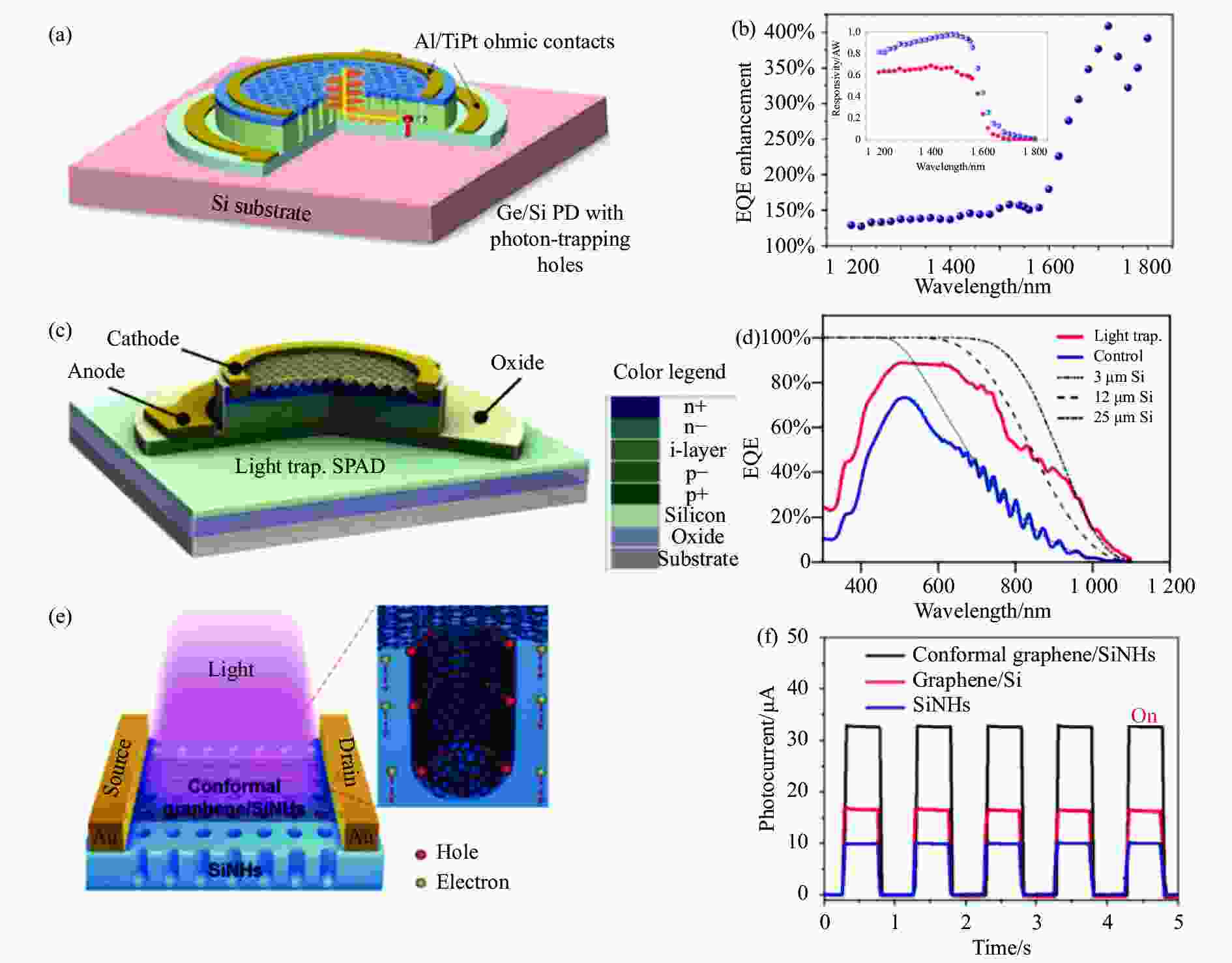
图 1 带有微孔阵列结构的硅基底红外探测器[19-21];(a)带有微孔阵列结构的锗硅光电器件的示意图[19];(b)锗硅器件在1 200~1 800 nm波段的外量子效率增强系数与响应度[19];(c)带有微孔阵列结构的硅单光子雪崩探测器的示意图[20];(d)不同尺寸硅单光子雪崩器件的外量子效率[20]共形石墨烯/硅纳米孔探测器的示意图[21];(f)测试得到的硅纳米孔、石墨烯/硅和共形石墨烯/硅纳米孔探测器的光电响应[21]
Figure 1. Infrared detectors with micro-holes on silicon substrates[19-21]; (a) Schematic diagram of Si-Ge optoelectronic device with micro-hole array structures[19]; (b) External quantum efficiency enhancement coefficient and responsivity in the 1 200-1 800 nm band of the Si-Ge device[19];(c) Schematic diagram of a silicon single-photon avalanche detector with micro-hole array structures[20]; (d) External quantum efficiency of devices of different sizes[20]; (e) Schematic diagram of conformal graphene/silicon nanopore detector[21] ; (f) Photoelectric response of silicon nanopore, graphene/silicon and conformal graphene/silicon nanopore detectors[21]
硅基微孔结构还可以和二维材料(如石墨烯)相结合,形成新型的高性能石墨烯/硅异质结光电探测器。中国科学院重庆绿色智能技术研究院的Yang[21]等人提出直接在硅纳米孔表面生长石墨烯的方法,显著改进了石墨烯/硅探测器的光吸收性能,如图1 (e)和(f)所示。该器件实现了高效的光捕获和优越的电子输运界面,获得了高达90%的高吸收率,显示出更高的光响应率(2720 A/W)和更快的响应速度(约6.2 μs)。
研究人员进一步系统研究了不同形貌和微孔阵列密度的微纳结构对探测器性能的影响。加州大学戴维斯分校的Gao等人[22]在硅探测器吸收层上刻蚀了方孔、六角孔、圆柱形和漏斗形等多种周期性微结构阵列,硅探测器在800~860 nm波段的外量子效率大于50%,器件示意图、刻蚀孔洞的SEM图和量子效率曲线如图2 (a)~(c) 所示。通过时域有限差分算法(FDTD)模拟了垂直光照下,漏斗形方型阵列和圆柱形小孔阵列的横向电场分布情况。对比发现,漏斗形阵列在横向的电场模式更强,更适合作为探测器的吸收增强结构。该校同一题组的C.Bartolo-Perez等人[23]研究了反向金字塔型、圆锥形等陷光结构以及单位面积微纳结构的数量对探测器量子效率的影响,提出一种同时大幅提高硅基光电探测器的响应灵敏度和响应速度的方法。通过优化陷光结构的设计并将其集成到高速光电探测器中,同时实现了高达1000%的宽波段吸收效率的增强和超过50%的电容值的降低,并获得了光电探测器的量子效率与陷光结构的数量、材料特性及加工工艺之间的关系,如图2 (d)~(f)所示。该方法克服了光电探测器探测效率和响应速度之间的矛盾,为高响应和高速度的CMOS集成接收器件的发展提供了新的思路。


图 2 (a)集成微纳小孔结构的硅光电二极管的示意图[22];(b)光电二极管中集成的不同形状孔洞的SEM图,包括方孔、六角孔、圆柱形和漏斗形[22];(c)光电二极管有源区域的扫描电子显微镜图片[22];(d)集成微结构的硅光电探测器的示意图[23];(e)漏斗型和反向金字塔型陷光结构的顶部和横截面视图[23];(f)外量子效率与纳米孔数量的关系[23]
Figure 2. (a) A schematic diagram of a silicon photodiode integrated with a micro-holes[22]; (b) SEM images of holes of different shapes integrated in the photodiode, including square holes, hexagonal holes, cylindrical and funnel shapes[22]; (c) Scanning electron microscope picture of the active area of the photodiode[22]; (d) A schematic diagram of a silicon photodetector with integrated micro structures[23]; (e) Top and cross-sectional views of the funnel-shaped and inverted pyramid-shaped light trapping structures[23]; (f) Relationship between the external quantum efficiency and the number of nano-holes[23]
介质型微纳结构在碲镉汞红外探测器上的增强效果同样十分显著。雷神公司研制了不同柱状结构和孔状结构的碲镉汞中波红外(截止波长5 μm)探测器[24],如图3所示,微结构化后在降低暗电流的同时不影响器件的量子效率。波士顿大学的Schuster等人[25]设计了一种新型限光结构碲镉汞中波红外探测器,将碲镉汞的衬底机械剥离后直接对碲镉汞的吸收层刻蚀形成表面微纳结构,不仅增强了宽波段吸收,还有效降低小尺寸阵列探测器间的串扰。

在各类介质型微纳结构中,除了微米尺度的孔和柱状微结构外,纳米线阵列也是一类用于增强红外探测器光学响应的重要结构。硅、锗和氧化锌等材料制备的纳米线阵列能表现出强烈的光子捕获效应,与其他光敏材料复合之后,通过多重反射与散射增强光敏吸收层中的局域光场,大幅度提升光敏材料的光吸收性能,并能拓展探测器的响应带宽。合肥工业大学的Luo 等人将甲基-硅纳米线阵列、等离子金纳米颗粒和石墨烯薄膜组合形成一种近红外光电探测器[26],如图4 (a)所示,开关比可以达到106,零偏压时的响应度和探测率分别是1.5 A/W和2.52×1014 cm·Hz1/2·W−1。该课题组还制作了另一种锗纳米锥(GeNCs)和硒化钯(PdSe2)多层膜组成的无需外部电源可以自驱动的红外光电探测器[27],图4 (b)所示,对1350 nm和1650 nm的入射光响应具有很高的灵敏度、稳定性和复现性,探测器的响应度和外量子效率分别达到了530.2 mA/W和42.4%。Liu等人[28]通过在垂直硅纳米线阵列上直接涂覆一层铯掺杂的甲酰亚胺碘化铅(FAPbl3)钙钛矿薄膜,制备了一种高灵敏度的近红外探测器。器件结构和光电响应如图4 (c)所示,在−0.9 V偏置电压下,响应度为844.33 mA/W,比探测率达到了3.2×1011 cm·Hz1/2·W−1。图4 (d)所示的是苏州大学Ning等人[29]提出一种在氧化锌纳米柱阵列上磁控溅射硫化钼薄膜制备高性能氧化锌-硫化钼光电探测器的方法。实验结果表明,该探测器表现出从紫外线到可见光和近红外的宽波段响应特征,相比氧化锌-硫化钼的平面异质结,该方法制作的纳米柱阵列光电探测器在相同光照下的光电流提升高达60倍。

图 4 不同类型的纳米柱近红外光电探测器的结构及光电特性[26-29]。(a)硅纳米线/金纳米颗粒/石墨烯探测器的I-V曲线和器件结构[26];(b)硅纳米线阵列/钙钛矿光电探测器的示意图(横截面图和850 nm入射光零偏压下的时间响应曲线)[27];(c) PbSe2/GeNcs阵列异质结光电探测器的示意图(锗纳米锥阵列的横截面SEM图和I-V曲线图)[28];(d) ZnO/MoS2光电探测器的结构示意图(SEM图和时间-电流响应)[29]
Figure 4. Structure and photoelectric characteristics of different types of nanorods near infrared photodetectors[26-29]. (a) I-V curve of the SiNW/Au/Graphene detector and the device structure[26]; (b) Schematic diagram of the silicon nanowire array/perovskite photodetector(cross-sectional view and 850 nm incident light time response curve under zero bias)[27]; (c) Schematic diagram of PbSe2/GeNcs array heterojunction photodetector(cross-sectional SEM image of germanium nanocone array and I-V curve diagram)[28]; (d) Schematic diagram of the ZnO/MoS2 detector(SEM images and time-current response)[29]
传统半导体器件受限于吸收层的厚度和界面反射导致的能量损耗,利用红外探测材料自身构建介质型微纳结构增强功能模块,能有效减小反射、提高传统探测器的量子效率,并在提高焦平面器件集成度方面具有较大优势。通过进一步控制微纳结构器件的制作成本和成品率,介质型微纳结构在各类红外探测器件中将有独特的应用价值。
-
入射光在表面金属微纳结构的激发下会产生表面等离激元,这是一种外界电磁场与金属表面自由电子相互作用产生的沿着金属表面传播的电磁振荡模式,可以在界面附近提高光子态密度,使得光探测效率得到极大的增强。在多种增强探测的技术中,表面等离激元具有突破衍射极限和局域增强的特性,为高性能光电探测器的研究提供了全新的研究方法。将表面金属结构与传统探测器相结合,可以极大地提升探测材料对光的吸收,从而产生更大的光电流,提高器件响应度[30-32]。
研究表明,通过设计表面金属微纳结构的周期、厚度等参数,可以控制共振吸收频率及响应光谱的宽度、强度。基本的方式是通过使用一维等离子体光栅将入射光耦合到探测器吸收层中来实现增强,海军实验室的Nolde等人实现了量子效率高达39%的低暗电流nBn中波红外光电探测器[33]。此外,多种形貌的表面金属结构被集成到各类不同的红外探测器中,实现了探测器性能的显著增强。密苏里科技大学的Cheng等人[34]基于非对称红外等离子体超材料实现了聚合物分子的超灵敏检测和表征,并对分子检测灵敏度和分子结构的相互作用进行了定量分析,如图5 (a)所示。通过利用等离子体激发的近场特性对分子吸收红外光谱信号的增强,最高可获得高达105的吸收增幅。

图 5 不同类型的表面金属微纳结构增强的红外探测器的结构与性能[34-37]。(a)非对称型红外等离子体探测器的结构示意图(SEM图和电场强度增强系数)[34];(b)十字星型等离子体双色红外探测器的结构示意图(SEM图和反射率曲线)[35];(c)方孔型等离子体长波红外探测器的结构示意图(SEM图和吸收增强系数曲线)[36];(d)等离子腔量子阱红外探测器的结构示意图(SEM图和吸收增强光谱)[37]
Figure 5. Structures and performances of enhanced infrared detectors with different types of surface metal microstructures[34-37]. (a) Structure diagram of the aysmmetric infrared plasma detector(SEM image and electric field intensity enhancement coefficient)[34] ; (b) Schematic diagram of the two-color infrared detector with cross stars(SEM image and reflection curve)[35];(c) Schematic diagram of the square-hole plasma long-wave infrared detector(SEM image and curve of absorption enhancement factor)[36]; (d) Schematic diagram of the plasma cavity quantum well infrared detector(SEM image and absorption enhancement spectrum)[37]
图5 (b)、(c)和(d)中分别显示了十字星形、方形和圆孔形金属超表面结构在双色红外探测器、多光谱偏振敏感中红外探测器和量子阱红外探测器中的应用示例及光电响应增强效果[35-37]。其中,图5 (b)中等离子体双色探测器的吸收率在两个探测波长处达到了~42.8%和46.2%,比非等离子体器件高20倍[35];图5 (c)中的光电探测器利用表面等离子体共振元件[36],具有可定制的频率响应和极化选择性,探测器的共振响应增强是无超表面探测器的5倍;而图5 (d)中的等离子体量子阱红外探测器[37]在8 μm的光响应达到了~7 A/W,峰值探测率高达7.4×1010 cm·Hz1/2·W−1。
表面金属微纳结构还能引起一类与上述等离激元效应不同的现象,即等离激元热电子效应。当与半导体接触的金属微纳结构受到外场激发时,产生的具有较高的能量的电子注入到半导体中,形成等离激元热电子。使用该效应的探测器可以突破半导体带隙限制,拓展器件的光响应范围[38-41]。此外,热电子的产生还可以提高光电流的大小,降低暗电流以及驰豫和复合过程中的能量损失,由此提高探测器的响应度、探测率和响应速度[42]。
利用金属等离子激元的热电子效应,典型的方式是将金属微纳结构集成在探测器的表面,表面等离子波衰减产生的热电子注入半导体材料,然后在电极作用下沿水平方向完成收集。莱斯大学的Knight等人将金纳米颗粒与n掺杂的硅接触,首次报道一种基于局域等离子体的等离激元热电子注入型的光电探测器[43],如图6 (a)所示,其探测波长约在1600 nm以内。
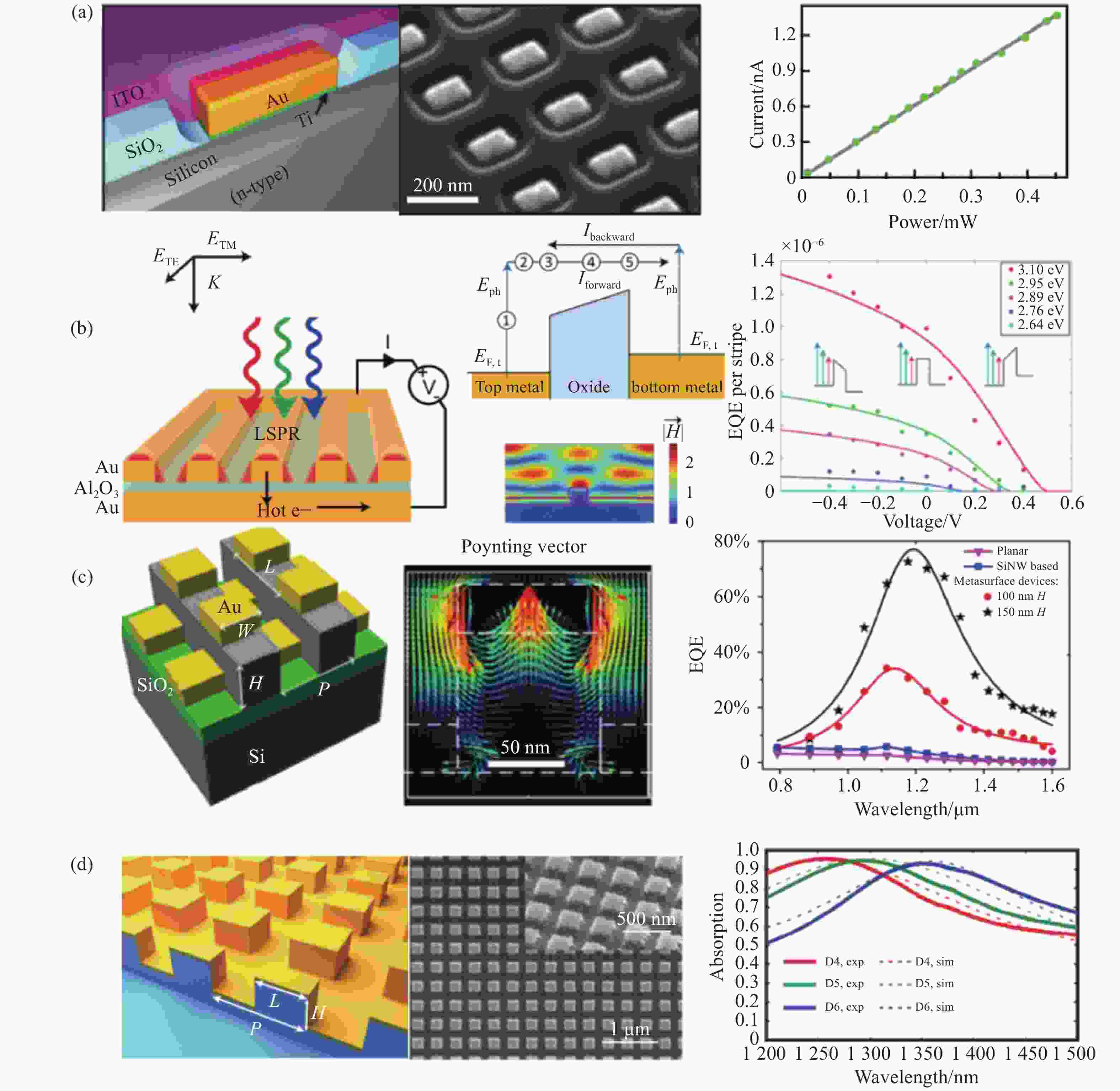
图 6 几类金属超表面热电子红外探测器的结构及其性能[43-46]。(a)局域等离激元热电子注入型的光电探测器的结构示意图、SEM图和光电性能[43];(b)基于表面等离子体的等离激元热电子光电探测器的结构示意图和量子效率曲线[44]; (c)全硅热电子型光电探测器结构示意图和光谱响应[45]; (d)一种宽带热电子光电探测器的结构示意图和吸收率曲线[46]
Figure 6. Structures and performance of several types of hot-electron infrared detectors with metal meta-surface[43-46] . (a) Structure diagram, SEM image and photoelectrical properties of local plasmon thermal electron injection photodetector[43]; (b) Structure diagram and quantum efficiency curve of plasmon thermoelectron photodetector based on surface plasma[44]; (c) Schematic diagram and spectral response of all-silicon thermoelectronic photodetector[45]; (d) Structure diagram and absorption curve of a wide band thermo-electron photodetector[46]
等离激元热电子不仅适用于局域等离子体,优化的表面等离子体激元结构也能表现出等离激元热电子注入现象。斯坦福大学的Chalabi等人[44]在两层金属之间用Al2O3作为势垒层,得到了基于表面等离子体的等离激元热电子注入型光电探测器,如图6 (b)所示。热电子器件的量子效率普遍很低,这是由于较低的电子注入和低光吸收率造成的。图6 (c)所示,复旦大学的Feng等人[45]提出了一种改进的全硅热电子型光电探测器结构,采用电子束光刻自对准技术,将特殊设计的超表面作为天线集成到绝缘体上的硅纳米线阵列中。该探测器在1.15 μm、480 nm带宽下的响应度和探测度分别高达94.5 mA/W和4.38 ×1011 cm·Hz1/2/W。其成功的关键主要有两个方面:一是利用专门设计的三维腔作为天线进行完美的吸收;二是在连接硅纳米线的顶部天线的下方通过等离子体的非辐射衰变产生热电子,并在高态密度硅纳米线中进行一维输运,以确保高注入效率。
图6 (d)所示为美国范德堡大学的Li等人[46]利用超薄等离子体纳米结构(厚度为15 nm,小于热电子扩散长度)与硅衬底集成,制作了一种宽带热电子光电探测器,通过设计超材料单元的几何形状可以调制探测器的光谱带宽和极化灵敏度,其光响应度是目前报道中最高的。
表面金属微纳结构增强型红外探测器在提高光吸收率、响应度、量子效率,降低暗电流和对响应光谱进行频率选择等方面具有更为明显的优势。虽然金属微纳结构制作工艺较为复杂,导致这类探测器距离规模量产和应用仍有一定距离,但随着微纳加工工艺的迭代,超表面等离子体和拓扑光子学等技术的发展,表面金属微纳结构在红外探测器中展现出很好的应用前景。
-
在增强红外探测器性能的微纳结构中,三维等离子腔体微结构另是一类重要的分支,对探测器性能的增强效果尤为显著。该结构是一种三维人工复合结构,是在金属超表面结构的基础上增加了底部反射层,两层之间的介质层作为探测器的吸收层。顶层的金属微纳结构同入射光发生相互作用产生偶极子共振,再与底平面反射层之间产生近场耦合效应,从而在吸收层中产生强烈的局域增强现象。早期这类结构主要用于单波段、多波段和宽波段等各类完美吸收器件的研究[47-49],近年来,随着微纳加工技术和仿真设计理论的不断成熟,三维等离子腔体微结构也越来越多地实际应用于红外探测器的光场增强领域。
如图7 (a)所示,美国桑迪亚国家实验室的Goldflam等人研制了一种集成十字星形金属纳米天线的II型超晶格长波红外探测器[50]。由底部金属电极、半导体层和表面纳米天线组成的等离子体腔之间的耦合使谐振波长处的吸收率显著增强,峰值量子效率提高到50%以上。同时吸收材料的变薄可以通过降低暗电流来降低光电探测器的噪声,提高长波红外探测器的比探测率。当探测元件的吸收区进一步降低至几百纳米的超薄层时,微结构探测器仍然能发挥极强的光吸收增强效应,使器件吸收率超过90%。美国杜克大学的Montoya等人[51]提出一种深亚波长超材料探测器体系结构,将多功能等离子谐振腔结构集成到一个超薄型(~/15λ,240 nm)InAs/GaSb II型超晶格(T2 SL)红外探测器上,如图7 (b)所示,从而显著提高了探测量子效率(QE)和对入射辐射的吸收。
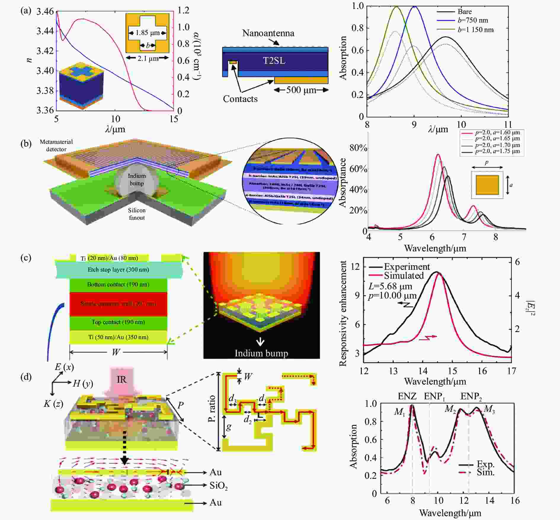
三维等离子腔结构还可以集成到量子阱红外探测器,利用微腔中的高度受限光学模式形成局域等离子体和量子阱之间的强耦合,从而增强光电转换过程。中国科学院上海技术物理研究所的Jing等人[52]制作出了第一个像素级等离子体微腔红外光电探测器,如图7 (c)所示,它在金属超表面和反射层之间集成了一个单量子阱,峰值响应度的增强幅度大于一个数量级。研究表明,像素大小对腔内局域等离子体和表面等离子体模式光耦合能力有不同的影响。随着像素宽度的减小,表面等离子体模式相对较弱,而腔模式仍然较强,对探测器性能增强起主导作用的是局域等离子体模式。图7 (d)所示为华中科技大学的Li等人[53]设计了一种适用于小像素尺寸焦平面阵列红外探测器的等离子腔超材料吸收器,它由深亚波长弯曲纳米天线、二氧化硅介质层和金背板组成。实验证明该器件具有11~14 μm双混合模式的高吸收光谱,像素间距为最小可达1.47 μm。通过等离子腔微结构的局域等离子体共振效应,在不影响吸收性能的情况下最小化了天线占用空间,为光电子器件集成小像素红外焦平面阵列以增强性能和扩展功能提供了可能性。
三维等离子腔微结构除了应用于上述传统的半导体材料红外探测器外,也被用于新型二维材料红外探测器的研究与应用中。如图8 (a)所示,中国科学院上海技术物理研究所的Guo等人[54]研究了集成二维材料石墨烯的等离子腔结构。根据不同的几何尺寸,该结构可以以磁谐振器形式或超表面索尔兹伯里屏幕形式工作。通过改变磁谐振器的结构形式,石墨烯等离子器件的吸收率在长波红外范围提高了4.2倍,器件的检测带宽扩大了3.6倍。

图 8 二维材料的等离子腔吸收增强结构和性能[54-56]。(a)石墨烯的等离子腔结构示意图及吸收曲线[54];(b)集成石墨烯薄膜的混合光栅法布里-珀罗结构示意图及吸收曲线[55];(c)黑磷的金纳米结构离子腔示意图和吸收曲线[56]
Figure 8. Structures and performance of plasmonic cavity enhanced 2D materials infrared detectors with micro-structure [54-56]. (a) Schematic diagram of plasma cavity structure and absorption curve of graphene[54]; (b) Schematic diagram and absorption curve of hybrid grating Fabry-Perot structure integrated with graphene film[55]; (c) Schematic diagram of gold nanostructure plasmonic cavity and absorption curve of black phosphorus[56]
华中科技大学的Zhou等人[55]提出了一种具有石墨烯薄膜的混合光栅法布里-珀罗结构,用于实现双波段窄带近红外光吸收,器件结构示意图与吸收率如图8 (b)所示。在正态入射时,由于导模共振和法布里-珀罗共振的临界耦合作用,器件存在两个近乎完美的窄带吸收峰,峰值波长处的局域吸光度分别从2.3%提高到75.25% (TM偏振)和82.61% (TE偏振)。图8 (c)中南加州大学的Audhkhasi等人[56]提出一种等离子腔模式的金纳米结构设计,用于在3.5 μm波长范围内增强黑磷薄膜的吸收。当薄膜厚度为5 nm时,在4 μm波长处的增强因子优化后可达561。这种在超薄介质层中实现强吸收增强的能力,加上黑磷独特的光电特性,使该设计在中红外光电探测器领域具有很好的应用潜力。
在三维等离子腔微结构中,金属层的作用至关重要。通常情况下金、银等贵金属被作为金属层,然而传统贵金属在中长红外波段具有较大的损耗,等离子腔微结构形成的局域光场很大一部分转化为金属的热能,不利于红外探测器光响应与量子效率的提高。近年来的研究表明,重掺半导体在红外波段的介电常数符合Drude模型,可以表现出类似金属的等离子体性质[57],但对红外光的损耗远小于金属材料。这使得无金属的全外延生长型等离子结构红外探测器件成为一个很有前景的研究方向,主要研究工作由美国德州大学奥斯汀分校的D.Wasserman课题组成员完成[58-60]。
该课题组的Nordin等人[61]提出并制作了一种集成重掺杂半导体的II类超晶格长波红外探测器结构,利用重掺半导体(掺杂浓度1 ×1019 cm−3)的金属等离子体特性形成共振腔,增强吸收谐振处的长波红外光。研究人员设计了两个目标吸收波长分别为8 μm和10 μm的探测器,吸收层总厚度分别只有1.42 μm和1.80 μm,如图9 (a)所示。两种器件的峰值外部量子效率分别达到了45%和27%。图9 (b)所示为Wang等人[62]提出了一种超薄型II类超晶格探测器结构。探测器红外吸收材料厚度为1/50波长,通过引入重掺杂型InAs和表面纳米天线结构,使谐振波长处的入射光局域在超薄吸收层中,实现了近50%的探测器吸收。随后,D.Wasserman课题组的Kamboj等人[63]又报道了一种全外延导模共振的中波红外II型超晶格nBn光探测器,如图9 (c)所示。该探测器包括一个高折射率吸收器/波导层,低折射率的半导体吸收层和重掺杂反射层。实验结果显示,在与导模共振耦合的波长处,吸收得到了强烈增强。对于吸收层厚度仅为250 nm 的TE偏振光,探测器在较高的工作温度(T=200 K),外部量子效率超过50%,探测率D*达到4 ×1010 cm·Hz1/2·W−1。
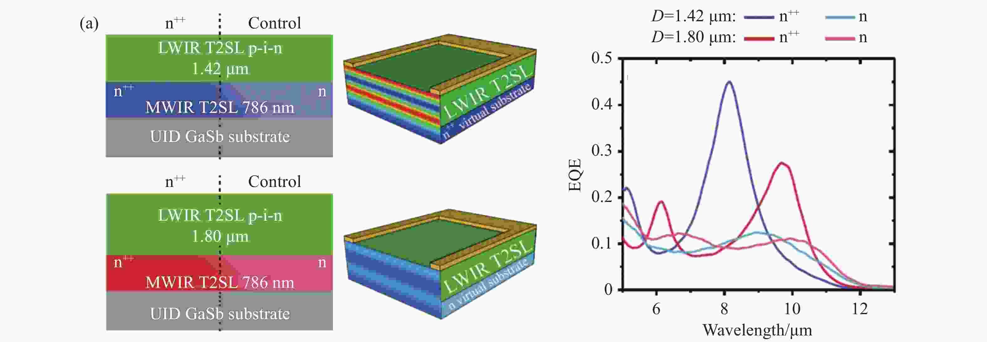

图 9 三种重掺半导体型等离子体探测器的结构和性能[61-63]。(a)重掺等离子腔探测器结构、电场分布及其EQE 曲线[61] ;(b) 超薄增强吸收长波红外探测器示意图(势垒层能带和吸收率曲线)[62]; (c) 单周期GMR 探测器示意图(横截面的扫描电子显微照片和探测率曲线)[63]
Figure 9. Structures and performance of three kinds of heavily doped semiconducting plasma detectors[61-63]. (a) Structures of heavily doped plasmonic detector, distribution of electrical field and curve of EQE[61]; (b) Schematic diagram of ultra-thin enhanced absorption long-wave infrared detector(band-structure schematics and the absorption curve)[62] ; (c) Schematic diagram of a single-cycle GMR detector (Scanning electron micrographs and detectability curves of cross-sections)[63]
重掺型半导体等离子体红外探测器避免了刻蚀衬底和蒸镀金属膜等工艺,可通过全外延法一次性生长,降低了工艺的复杂性。但半导体重掺工艺本身具有较高的技术难度,重掺元素难以有效激活,导致该方法的成品率不高。整体上看,三维等离子体腔微结构红外探测器的研究还处在探索阶段,物理机理和制作工艺都有待进一步深入研究。
-
利用微纳结构实现对红外探测器光电性能的多维度调控及其机理研究是当前红外探测器研究的前沿,也是未来新一代红外探测器发展的重要方向。文中根据增强红外探测器的微纳结构特点和增强机理的不同,从介质型、表面金属型、三维等离子腔体型等方面概述了基于微纳结构增强的红外探测器的最新研究进展,阐述了微纳结构增强探测器性能的机理及主要方法,不同探测器的结构类型、原理以及关键指标总结如表1所示。
表 1 微纳结构增强型红外探测器分类和进展
Table 1. Classification and progress of micro-nano structure enhanced infrared detectors
Structure type Principle Wavelength
/μmResponsivity/(A/W) D*/cm·Hz1/2·W−1
DielectricSilicon substrate Increasing the effective propagation path by multiple reflections and scatterings 0.8-1.8[19-23] 0.91[19] 1.25×10¹¹ [21] HgCdTe 1-5[24] 1-2[24] NETD:50 mK[24] Nanowires 1-1.65[26] 1.5[26] 2.52×10¹⁴ [26]
Surface metalMeta-surface SPP and LSP are excited at resonant wavelength to improve optical field density and enhance the absorption; 3-12[34-37] 7 [37] 7.4×10¹⁰ [37] LSP hot electrons 1.2~1.6[43] 8×10⁻⁶[43] 2.4×10⁷ [46] SPP hot electrons 0.8-1.6[45] 9×10⁻²[45] 4.38 ×10¹¹[45]
3D plasma cavitySemi-conductor cavity Strong local enhancement and near-field coupling effect in the absorption layer of multi-layer cavity 4-11[51] 2[51] 6.06 ×10¹⁰ [51] Quantum well cavity 11-14[52] 0.6[52] 8.52 ×10⁹ [52] 2D material cavity 3-14[54-56] 0.32[55] —— 尽管近年来人们在微纳结构增强红外探测器性能方面开展了系列研究,并取得了阶段性进展,但微纳结构红外探测器件仍面临一些困难和挑战亟需克服。
(1)工艺的兼容性问题。微纳结构的制备在实验室可采用电子束光刻(EBL)和聚焦离子束光刻(FIB)等加工工艺,但复杂的结构在向传统半导体生产线导入时,由于材料、镀膜、光刻、刻蚀等工艺的兼容性问题,在产品化过程中面临较大挑战。
(2)性能的颠覆性不够。微结构红外探测器的响应波段、响应度、噪声、响应速度等性能指标之间依然存在相互制约关系,虽然特定的某个性能可以通过优化设计进行提升,但一般会引起综合性能的降低,导致器件性能的颠覆性和综合竞争力不足。
(3)自适应能力有待提升。微纳结构的材料和结构一旦确定,其功能往往也固定下来。现有的微纳结构增强型红外探测器或功能单一,或响应光谱受限,面临复杂应用场景时动态调节能力和适应性还达不到预期。
围绕上述问题,微纳结构增强型红外探测器件在未来发展中需要重点关注以下研究方向:
(1)与CMOS兼容的微结构探测器件结构设计方法与加工工艺。在原有数字CMOS工艺基础上研发适合微纳结构红外探测器的深亚微米CMOS工艺,优化工艺流程,提高探测器与运算电路集成的工艺兼容性,为基于商用CMOS工艺的微纳结构红外光电探测器的实现提供解决方案。
(2)同时具备宽波段、高灵敏度、低噪声和高响应速度等综合性能的微纳结构红外探测技术。在增强微纳结构与入射光场宽光谱上相互作用,提高光吸收效率和光谱响应带宽的基础上,同时抑制暗电流抑制,提升探测器响应速度和灵敏度,全面提升器件的综合性能。
(3)响应光谱等性能具有动态调控能力的自适应型器件。拓展微结构红外探测器件响应光谱频率的动态选择范围,并将电子逻辑处理、智能控制和运算存储等多种功能模块高度集成,增加探测器的灵活性和适用性,对于微结构红外探测器的设计和应用具有重要意义。
从实现途径上来说,主要是研发新工艺方法、引入新物理机理和采用新材料/新设计。在研发新工艺方法方面,可变电容、浅沟槽隔离和深n阱的引入将克服传统CMOS工艺的局限性,减少噪声耦合并隔离串扰,使亚微米CMOS工艺更兼容微纳结构红外探测器的加工;重掺型等离子结构全外延生长法的提出将为增强微纳结构与红外探测器的兼容性提供一种有效方式,有望实现了对探测器性能和成本的兼顾。在引入新物理机理方面,等离激元热电子注入、拓扑光子学和人工智能深度学习与微纳结构设计的相互结合将为综合性能颠覆性提升的微纳结构红外探测器的实现提供了新的可能。在采用新材料和新设计方面,压控、温控和相变等材料的引入则能实现对微纳结构探测器光谱响应的动态调控,智能处理芯片片内集成、读出电路三维垂直互联和高效能稀疏神经网络等技术的引入将有望实现感算一体的多功能微纳结构探测器,提升其在各种应用场景的适应性。
可以预见,随着未来探测器新材料、新结构、新机理的深入研究和系统集成工艺的不断进步,微纳结构增强型红外探测器将展现出极具前景的应用潜力,为高集成度、高性能和低成本的红外探测系统提供新的解决方案。
Research progress of micro-nano structures enhanced infrared detectors (Invited)
-
摘要: 红外探测器在军事侦查、遥感、通信、精确制导和航空航天等领域发挥着关键作用,受到世界各国长期关注,具有重要的研究价值和应用前景。微纳结构与传统半导体探测器集成后能够有效提高光子耦合效率和等效光程,突破传统体材料的吸收极限,提高光电器件的量子效率并降低器件的暗电流,为高性能红外探测器的研究提供了全新的技术手段。文中围绕近年来各种不同类型的微纳结构增强型红外探测器的研究展开综述。首先,介绍了微纳结构增强型红外探测器的基本原理,根据微纳结构的材料和功能不同,进行了分类和对比;其次,分别从介质型、表面金属型和三维等离子腔型等方面对微纳结构在红外探测器上的研究进展进行了阐述;最后,对基于微纳结构增强型红外探器的发展趋势进行了总结和展望。Abstract: Infrared detectors play an important role in the areas of military investigation, remote sensing, communication, precision guidance and aerospace, which have been concerned by the world for a long time and have high research value and good application prospect. The integration of micro-nano structures and traditional semiconductor detector can effectively improve the photon coupling efficiency and equivalent optical path, exceed the absorption limit of traditional bulk materials, improve the quantum efficiency of photoelectric devices and reduce the dark current of devices, providing a new technical means for the research of high-performance infrared detectors. Various types of enhanced infrared photodetectors with micro-nano structures were reviewed in this paper. Firstly, the basic principle of performance enhancd infrared detectors with micro-nano structures were introduced. According to the different materials and functions of micro-nano structures, it was classified and compared; Secondly, the research progress of the above micro-nano structures in infrared detectors were systematically demonstrated from the aspects of dielectric type, surface metal type and 3D plasma cavity type. Finally, the development trend of infrared detector based on micro-nano structure enhancement was prospected.
-
Key words:
- infrared detection /
- micro-nano structure /
- light trapping /
- local enhancement /
- plasma plasmon
-
图 1 带有微孔阵列结构的硅基底红外探测器[19-21];(a)带有微孔阵列结构的锗硅光电器件的示意图[19];(b)锗硅器件在1 200~1 800 nm波段的外量子效率增强系数与响应度[19];(c)带有微孔阵列结构的硅单光子雪崩探测器的示意图[20];(d)不同尺寸硅单光子雪崩器件的外量子效率[20]共形石墨烯/硅纳米孔探测器的示意图[21];(f)测试得到的硅纳米孔、石墨烯/硅和共形石墨烯/硅纳米孔探测器的光电响应[21]
Figure 1. Infrared detectors with micro-holes on silicon substrates[19-21]; (a) Schematic diagram of Si-Ge optoelectronic device with micro-hole array structures[19]; (b) External quantum efficiency enhancement coefficient and responsivity in the 1 200-1 800 nm band of the Si-Ge device[19];(c) Schematic diagram of a silicon single-photon avalanche detector with micro-hole array structures[20]; (d) External quantum efficiency of devices of different sizes[20]; (e) Schematic diagram of conformal graphene/silicon nanopore detector[21] ; (f) Photoelectric response of silicon nanopore, graphene/silicon and conformal graphene/silicon nanopore detectors[21]
图 2 (a)集成微纳小孔结构的硅光电二极管的示意图[22];(b)光电二极管中集成的不同形状孔洞的SEM图,包括方孔、六角孔、圆柱形和漏斗形[22];(c)光电二极管有源区域的扫描电子显微镜图片[22];(d)集成微结构的硅光电探测器的示意图[23];(e)漏斗型和反向金字塔型陷光结构的顶部和横截面视图[23];(f)外量子效率与纳米孔数量的关系[23]
Figure 2. (a) A schematic diagram of a silicon photodiode integrated with a micro-holes[22]; (b) SEM images of holes of different shapes integrated in the photodiode, including square holes, hexagonal holes, cylindrical and funnel shapes[22]; (c) Scanning electron microscope picture of the active area of the photodiode[22]; (d) A schematic diagram of a silicon photodetector with integrated micro structures[23]; (e) Top and cross-sectional views of the funnel-shaped and inverted pyramid-shaped light trapping structures[23]; (f) Relationship between the external quantum efficiency and the number of nano-holes[23]
图 4 不同类型的纳米柱近红外光电探测器的结构及光电特性[26-29]。(a)硅纳米线/金纳米颗粒/石墨烯探测器的I-V曲线和器件结构[26];(b)硅纳米线阵列/钙钛矿光电探测器的示意图(横截面图和850 nm入射光零偏压下的时间响应曲线)[27];(c) PbSe2/GeNcs阵列异质结光电探测器的示意图(锗纳米锥阵列的横截面SEM图和I-V曲线图)[28];(d) ZnO/MoS2光电探测器的结构示意图(SEM图和时间-电流响应)[29]
Figure 4. Structure and photoelectric characteristics of different types of nanorods near infrared photodetectors[26-29]. (a) I-V curve of the SiNW/Au/Graphene detector and the device structure[26]; (b) Schematic diagram of the silicon nanowire array/perovskite photodetector(cross-sectional view and 850 nm incident light time response curve under zero bias)[27]; (c) Schematic diagram of PbSe2/GeNcs array heterojunction photodetector(cross-sectional SEM image of germanium nanocone array and I-V curve diagram)[28]; (d) Schematic diagram of the ZnO/MoS2 detector(SEM images and time-current response)[29]
图 5 不同类型的表面金属微纳结构增强的红外探测器的结构与性能[34-37]。(a)非对称型红外等离子体探测器的结构示意图(SEM图和电场强度增强系数)[34];(b)十字星型等离子体双色红外探测器的结构示意图(SEM图和反射率曲线)[35];(c)方孔型等离子体长波红外探测器的结构示意图(SEM图和吸收增强系数曲线)[36];(d)等离子腔量子阱红外探测器的结构示意图(SEM图和吸收增强光谱)[37]
Figure 5. Structures and performances of enhanced infrared detectors with different types of surface metal microstructures[34-37]. (a) Structure diagram of the aysmmetric infrared plasma detector(SEM image and electric field intensity enhancement coefficient)[34] ; (b) Schematic diagram of the two-color infrared detector with cross stars(SEM image and reflection curve)[35];(c) Schematic diagram of the square-hole plasma long-wave infrared detector(SEM image and curve of absorption enhancement factor)[36]; (d) Schematic diagram of the plasma cavity quantum well infrared detector(SEM image and absorption enhancement spectrum)[37]
图 6 几类金属超表面热电子红外探测器的结构及其性能[43-46]。(a)局域等离激元热电子注入型的光电探测器的结构示意图、SEM图和光电性能[43];(b)基于表面等离子体的等离激元热电子光电探测器的结构示意图和量子效率曲线[44]; (c)全硅热电子型光电探测器结构示意图和光谱响应[45]; (d)一种宽带热电子光电探测器的结构示意图和吸收率曲线[46]
Figure 6. Structures and performance of several types of hot-electron infrared detectors with metal meta-surface[43-46] . (a) Structure diagram, SEM image and photoelectrical properties of local plasmon thermal electron injection photodetector[43]; (b) Structure diagram and quantum efficiency curve of plasmon thermoelectron photodetector based on surface plasma[44]; (c) Schematic diagram and spectral response of all-silicon thermoelectronic photodetector[45]; (d) Structure diagram and absorption curve of a wide band thermo-electron photodetector[46]
图 8 二维材料的等离子腔吸收增强结构和性能[54-56]。(a)石墨烯的等离子腔结构示意图及吸收曲线[54];(b)集成石墨烯薄膜的混合光栅法布里-珀罗结构示意图及吸收曲线[55];(c)黑磷的金纳米结构离子腔示意图和吸收曲线[56]
Figure 8. Structures and performance of plasmonic cavity enhanced 2D materials infrared detectors with micro-structure [54-56]. (a) Schematic diagram of plasma cavity structure and absorption curve of graphene[54]; (b) Schematic diagram and absorption curve of hybrid grating Fabry-Perot structure integrated with graphene film[55]; (c) Schematic diagram of gold nanostructure plasmonic cavity and absorption curve of black phosphorus[56]
图 9 三种重掺半导体型等离子体探测器的结构和性能[61-63]。(a)重掺等离子腔探测器结构、电场分布及其EQE 曲线[61] ;(b) 超薄增强吸收长波红外探测器示意图(势垒层能带和吸收率曲线)[62]; (c) 单周期GMR 探测器示意图(横截面的扫描电子显微照片和探测率曲线)[63]
Figure 9. Structures and performance of three kinds of heavily doped semiconducting plasma detectors[61-63]. (a) Structures of heavily doped plasmonic detector, distribution of electrical field and curve of EQE[61]; (b) Schematic diagram of ultra-thin enhanced absorption long-wave infrared detector(band-structure schematics and the absorption curve)[62] ; (c) Schematic diagram of a single-cycle GMR detector (Scanning electron micrographs and detectability curves of cross-sections)[63]
表 1 微纳结构增强型红外探测器分类和进展
Table 1. Classification and progress of micro-nano structure enhanced infrared detectors
Structure type Principle Wavelength
/μmResponsivity/(A/W) D*/cm·Hz1/2·W−1
DielectricSilicon substrate Increasing the effective propagation path by multiple reflections and scatterings 0.8-1.8[19-23] 0.91[19] 1.25×10¹¹ [21] HgCdTe 1-5[24] 1-2[24] NETD:50 mK[24] Nanowires 1-1.65[26] 1.5[26] 2.52×10¹⁴ [26]
Surface metalMeta-surface SPP and LSP are excited at resonant wavelength to improve optical field density and enhance the absorption; 3-12[34-37] 7 [37] 7.4×10¹⁰ [37] LSP hot electrons 1.2~1.6[43] 8×10⁻⁶[43] 2.4×10⁷ [46] SPP hot electrons 0.8-1.6[45] 9×10⁻²[45] 4.38 ×10¹¹[45]
3D plasma cavitySemi-conductor cavity Strong local enhancement and near-field coupling effect in the absorption layer of multi-layer cavity 4-11[51] 2[51] 6.06 ×10¹⁰ [51] Quantum well cavity 11-14[52] 0.6[52] 8.52 ×10⁹ [52] 2D material cavity 3-14[54-56] 0.32[55] ——  下载: 导出CSV
-
[1] Wang J, Fang H, Wang X, et al. Recent progress on localized field enhanced two-dimensional material photodetectors from ultraviolet-visible to infrared [J]. Small, 2017, 13(35): 1700894. doi: 10.1002/smll.201700894 [2] Guan X, Yu X, Periyanagounder D, et al. Recent progress in short-to long-wave infrared photodetection using 2D materials and heterostructures [J]. Advanced Optical Materials, 2021, 9: 2001708. doi: 10.1002/adom.202001708 [3] Hu X, Wu J, Wu M, et al. Recent developments of infrared photodetectors with low-dimensional inorganic nanostructures [J]. Nano Research, 2021,15(2): 1-13. [4] Jiang F, Shi M, Zhou J, et al. Integrated photonic structure enhanced infrared photodetectors [J]. Advanced Photonics Research, 2021, 2(9): 2000187. doi: 10.1002/adpr.202000187 [5] Zhang T, Wang S J, Zhang X Y, et al. Recent progress on nanostructure-based broadband absorbers and their solar energy thermal utilization [J]. Frontiers of Chemical Science and Engineering, 2021, 15(1): 35-48. doi: 10.1007/s11705-020-1937-6 [6] Zhuge F, Zheng Z, Luo P, et al. Nanostructured materials and architectures for advanced infrared photodetection [J]. Advanced Materials Technologies, 2017, 2(8): 1700005. doi: 10.1002/admt.201700005 [7] Anguita J V, Ahmad M, Haq S, et al. Ultra-broadband light trapping using nanotextured decoupled graphene multilayers [J]. Science Advances, 2016, 2(2): e1501238. doi: 10.1126/sciadv.1501238 [8] Wang H, Zhen H, Li S, et al. Self-rolling and light-trapping in flexible quantum well–embedded nanomembranes for wide-angle infrared photodetectors [J]. Science Advances, 2016, 2(8): e1600027. doi: 10.1126/sciadv.1600027 [9] Lin X, Ding Z Y, Wang W P, et al. Investigation on the operation enhancement of HgCdTe photon-trapping detector [J]. Laser & Infrared, 2017, 47(12): 1510-1515. (in Chinese) [10] Lee S C, Krishna S, Brueck S R J, et al. Light direction-dependent plasmonic enhancement in quantum dot infrared photodetectors [J]. Applied Physics Letters, 2010, 97(2): 21112. doi: 10.1063/1.3454776 [11] Oay A, Avt A, Vvk A, et al. Planar plasmonic nanocavity for efficient enhancement of photoluminescence of molecular emitters [J]. Optical Materials, 2019, 94: 348-355. doi: 10.1016/j.optmat.2019.06.015 [12] Lee S C, Krishna S, Brueck S R J, et al. Beyond the yablonovitch limit: Trapping light by frequency shift [J]. Applied Physics Letters, 2011, 98(7): 71107. doi: 10.1063/1.3554436 [13] Prajapati A, Chauhan A, Keizman D, et al. Approaching the Yablonovitch limit with free-floating arrays of subwavelength trumpet non-imaging light concentrators driven by extraordinary low transmission [J]. Nanoscale, 2019, 11(8): 3681-3688. doi: 10.1039/C8NR10381J [14] Yokogawa S, Oshiyama I, Ikeda H, et al. IR sensitivity enhancement of CMOS Image Sensor with diffractive light trapping pixels [J]. Sci Rep, 2017, 7(1): 3832. doi: 10.1038/s41598-017-04200-y [15] Fang Z. Plasmonic silicon quantum dots extend photodetection into mid-infrared range [J]. Science Bulletin, 2017, 62(21): 8-9. [16] Tong J, Tobing L, Luo Y, et al. Single plasmonic structure enhanced dual-band room temperature infrared photodetection [J]. Scientific Reports, 2018, 8(1): 1548. doi: 10.1038/s41598-018-20028-6 [17] Hu W D, Ge H, Xie R, et al. Skin effect photon-trapping enhancement in infrared photodiodes [J]. Optics Express, 2021, 29(15): 22823-22837. doi: 10.1364/OE.427714 [18] Ye Z H, Zhang P, Li Y, et al. Photon trapping photodiode design in HgCdTe mid-wavelength infrared focal plane array detectors [J]. Optical & Quantum Electronics, 2014, 46(10): 1385-1390. [19] Cansizoglu H, Bartolo-Perez C, Gao Y, et al. Surface-illuminated photon-trapping high-speed Ge-on-Si photodiodes with improved efficiency up to 1700 nm [J]. Photonics Research, 2018, 6(7): 734-742. doi: 10.1364/PRJ.6.000734 [20] Zang K, Jiang X, Huo Y, et al. Silicon single-photon avalanche diodes with nano-structured light trapping [J]. Nature Communications, 2017, 8(1): 628. doi: 10.1038/s41467-017-00733-y [21] Yang J, Tang L, Luo W, et al. Light trapping in conformal graphene/silicon nanoholes for high performance photodetectors [J]. ACS Applied Materials & Interfaces, 2019, 11(33): 30421-30429. [22] Gao Y, Cansizoglu H, Polat K G, et al. Photon-trapping microstructures enable high-speed high-efficiency silicon photodiodes [J]. Nature Photonics, 2017, 11(5): 301-308. doi: 10.1038/nphoton.2017.37 [23] Bartolo-Perez C, Qarony W, Ghandiparsi S, et al. Maximizing absorption in photon trapping ultra-fast silicon photodetectors [J]. Advanced Photonics Research, 2021, 2(6): 2000190. doi: 10.1002/adpr.202000190 [24] Wehner J, Smith E, Venzor G M, et al. HgCdTe photon trapping structure for broadband mid-wavelength infrared absorption [J]. Journal of Electronic Materials, 2011, 40(8): 1840-1846. doi: 10.1007/s11664-011-1703-0 [25] Schuster J, Bellotti E. Numerical simulation of crosstalk in reduced pitch HgCdTe photon-trapping structure pixel arrays [J]. Optics Express, 2013, 21(12): 14712-14727. doi: 10.1364/OE.21.014712 [26] Luo L B, Zeng L H, Chao X, et al. Light trapping and surface plasmon enhanced high-performance NIR photodetector [J]. Scientific Reports, 2014, 4(1): 3914. [27] Linbao L, Di W, Chao X, et al. PdSe2 multilayer on germanium nanocones array with light trapping effect for sensitive infrared photodetector and image sensing application [J]. Advanced Functional Materials, 2019, 29(22): 1900849. [28] Liu J Q, Yang G, Wu G, et al. Silicon/perovskite core-shell heterojunctions with light trapping effect for sensitive self-driven NIR photodetectors [J]. ACS Applied Materials & Interfaces, 2018, 10(33): 27850-27857. [29] Ning L, Jiang T H, Shao Z B, et al. Light-trapping enhanced ZnO-MoS2 core-shell nanopillar arrays for broadband ultraviolet-visible-near infrared photodetection [J]. Journal of Materials Chemistry C Materials for Optical & Electronic Devices, 2018, 6(26): 7077-7084. [30] Nordin L, Li K, Briggs A, et al. Enhanced emission from ultra-thin long wavelength infrared superlattices on epitaxial plasmonic materials [J]. Applied Physics Letters, 2020, 116(2): 021102. doi: 10.1063/1.5132311 [31] Yang J, Zhu Z, Zhang J, et al. Mie resonance induced broadband near-perfect absorption in nonstructured graphene loaded with periodical dielectric wires [J]. Optics Express, 2018, 26(16): 20174-20182. doi: 10.1364/OE.26.020174 [32] Meng J, Cadusch J J, Crozier K B. Plasmonic mid-infrared filter array-detector array chemical classifier based on machine learning [J]. ACS Photonics, 2021, 8(2): 648-657. doi: 10.1021/acsphotonics.0c01786 [33] Nolde J A, Kim M, Kim C S, et al. Resonant quantum efficiency enhancement of midwave infrared nBn photodetectors using one-dimensional plasmonic gratings [J]. Applied Physics Letters, 2015, 106(26): 261109. doi: 10.1063/1.4923404 [34] Cheng F, Yang X, Gao J. Ultrasensitive detection and characterization of molecules with infrared plasmonic metamaterials [J]. Scientific Reports, 2015, 5(1): 14327. doi: 10.1038/srep14327 [35] Mao F, Xie J, Xiao S, et al. Plasmonic light harvesting for multicolor infrared thermal detection [J]. Optics Express, 2013, 21(1): 295. doi: 10.1364/OE.21.000295 [36] Jessie R, Shenoi R V, Sanjay K, et al. Design of plasmonic photonic crystal resonant cavities for polarization sensitive infrared photodetectors [J]. Optics Express, 2010, 18(4): 3672-3686. doi: 10.1364/OE.18.003672 [37] Wei W, Bonakdar A, Mohseni H. Plasmonic enhanced quantum well infrared photodetector with high detectivity [J]. Applied Physics Letters, 2010, 96(16): 667. [38] Zheng B, Zhao H, Manjavacas A, et al. Distinguishing between plasmon-induced and photoexcited carriers in a device geometry [J]. Nature Communications, 2015, 6(1): 7797. doi: 10.1038/ncomms8797 [39] Xia F, Wang H, Xiao D, et al. Two-dimensional material nanophotonic [J]. Nature Photonics, 2014, 8(12): 899-907. doi: 10.1038/nphoton.2014.271 [40] Narang P, Sundararaman R, Atwater H A. Plasmonic hot carrier dynamics in solid-state and chemical systems for energy conversion [J]. Nanophotonics, 2016, 5(1): 96-111. doi: 10.1515/nanoph-2016-0007 [41] Brongersma M L, Halas N J, Nordlander P. Plasmon-induced hot carrier science and technology [J]. Nature Nanotechnology, 2015, 10(1): 25-34. doi: 10.1038/nnano.2014.311 [42] Wang W, Klots A, Prasai D, et al. Hot electron-based near-infrared photodetection using bilayer MoS2 [J]. Nano Letters, 2015, 15(11): 7440-7444. doi: 10.1021/acs.nanolett.5b02866 [43] Knight M W, Sobhani H, Nordlander P, et al. Photodetection with active optical antennas [J]. Science, 2011, 332(6030): 702-704. doi: 10.1126/science.1203056 [44] Chalabi H, Schoen D, Brongersma M L. Hot-electron photodetection with a plasmonic nanostripe antenna [J]. Nano Letters, 2014, 14(3): 1374-1380. doi: 10.1021/nl4044373 [45] Feng B, Zhu J, Bingrui L U, et al. Achieving infrared detection by all-Si plasmonic hot-electron detectors with high detectivity [J]. ACS Nano, 2019, 13(7): 8433-8441. [46] Li W, Valentine J. Metamaterial perfect absorber based hot electron photodetection [J]. Nano Letters, 2012, 14(6): 3510-3514. [47] Bouchon P, Koechlin C, Pardo F, et al. Wideband omni-directional infrared absorber with a patchwork of plasmonic nanoantennas [J]. Optics Letters, 2012, 37(6): 1038. doi: 10.1364/OL.37.001038 [48] Cui, Y X, Xu J, Fung K H, et al. A thin film broadband absorber based on multi-sized nanoantennas. [J]. Applied Physics Letters, 2011, 99(25): 253101. doi: 10.1063/1.3672002 [49] Feng R, Ding W, Liu L, et al. Dual-band infrared perfect absorber based on asymmetric T-shaped plasmonic array [J]. Optics Express, 2014, 22(S2): A335-A343. doi: 10.1364/OE.22.00A335 [50] Goldflam M, Kadlec E A, Olson B V, et al. Enhanced infrared detectors using resonant structures combined with thin type-II superlattice absorbers [J]. Applied Physics Letters, 2016, 109(25): 251103. doi: 10.1063/1.4972844 [51] Montoya J A, Tian Z B, Krishna S, et al. Ultra-thin infrared metamaterial detector for multicolor imaging applications [J]. Optics Express, 2017, 25(19): 23343. doi: 10.1364/OE.25.023343 [52] Jing Y L, Li Z F, Li Q, et al. Pixel-level plasmonic microcavity infrared photodetector [J]. Scientific Reports, 2016, 6(1): 25849. doi: 10.1038/srep25849 [53] Li J, Li J Z, Zhou H, et al. Plasmonic metamaterial absorbers upon strong coupling effects for small pixel infrared detector [J]. Optics Express, 2021, 29(15): 22907-22921. doi: 10.1364/OE.430156 [54] Guo S, Deng J, Zhou J, et al. Combined role of polarization matching and critical coupling in enhanced absorption of 2 D materials based on metamaterials [J]. Optics Express, 2021, 29(6): 9269-9282. doi: 10.1364/OE.419028 [55] Zhou K, Cheng Q, Lu L, et al. Dual-band tunable narrowband near-infrared light trapping control based on a hybrid grating-based Fabry–Perot structure [J]. Optics Express, 2020, 28(2): 1647-1656. doi: 10.1364/OE.383988 [56] Audhkhasi R, Povinelli M L. Gold-black phosphorus nano-structured absorbers for efficient light trapping in the mid-infrared [J]. Optics Express, 2020, 28(13): 19562-19570. doi: 10.1364/OE.398641 [57] Felts J R, Law S, Roberts C M, et al. Near-field infrared absorption of plasmonic semiconductor microparticles studied using atomic force microscope infrared spectroscopy [J]. Applied Physics Letters, 2013, 102(15): 152110. doi: 10.1063/1.4802211 [58] Law S, Liu R, Wasserman D. Doped semiconductors with band-edge plasma frequencies [J]. Journal of Vacuum Science & Technology B, 2014, 32(5): 052601. [59] Qian X, Vangala S, Wasserman D, et al. High-optical-quality nanosphere lithographically formed InGaAs quantum dots using molecular beam epitaxy assisted GaAs mass transport and overgrowth [J]. Journal of Vacuum Science & Technology B, 2010, 28(3): C3C9-C3C14. [60] Xu X, Kwon H, Finch S, et al. Reflecting metagrating-enhanced thin-film organic light emitting devices [J]. Applied Physics Letters, 2021, 118(5): 053302. doi: 10.1063/5.0034573 [61] Nordin L, Kamboj A, Petluru P, et al. All-epitaxial integration of long-wavelength infrared plasmonic materials and detectors for enhanced responsivity [J]. ACS Photonics, 2020, 7(8): 1950-1956. doi: 10.1021/acsphotonics.0c00659 [62] Wang S H, Yoon N, Kamboj A, et al. Ultra-thin enhanced-absorption long-wave infrared detectors [J]. Applied Physics Letters, 2018, 112(9): 091104. doi: 10.1063/1.5017704 [63] Kamboj A, Nordin L, Petluru P, et al. All-epitaxial guided-mode resonance mid-wave infrared detectors [J]. Applied Physics Letters, 2021, 118(20): 201102. doi: 10.1063/5.0047534 -

 点击查看大图

计量
- 文章访问数: 733
- HTML全文浏览量: 132
- PDF下载量: 290
- 被引次数: 0

