


-
光谱仪器是物质化学组成及含量的重要分析仪器,已在现代科学实验、生物医学、工农业生产、国防等领域得到广泛的应用。传统光谱仪器使用条件苛刻、体积庞大,因而大大地限制了其应用范围。芯片式光谱仪的出现解决了尺寸过大带来的系列问题,但光束的传输主要还是依靠光纤来进行[1-5]。
为解决芯片式光谱仪与光纤的耦合问题,国内外研究人员提出许多方案,目前应用最广的方案是通格衍射原理,将光纤输入的光束衍射到水平方向,耦合进波导中去。但上述耦合方式由于光栅耦合器与光纤接触会造成磨损;由于光纤本身的遮挡导致无法观测到其对准情况;且不同类型的芯片式光谱仪的光栅耦合器与光纤端面尺寸不匹配导致能量损耗[6-11]。
若增大光纤与芯片式光谱仪之间的距离,虽然能够解决芯片式光谱仪的磨损和遮挡问题,但是由于光纤传输的光发散角较大,而光栅耦合器尺寸在微米级别,当光传输到芯片式光谱仪时光斑远大于光栅耦合器尺寸,耦合效果不好,且对准精度要求高,每次进行光束耦合及监测时都需利用六维调节架反复调节光纤位置,成本极高[12]。
针对芯片式光谱仪的耦合及监测,文中提出了一种芯片式光谱仪光束耦合与对准监测集成光学系统。该系统有效解决了尺寸不匹配、芯片磨损、调节困难等问题,且能够对耦合效果进行实时监测。为芯片式光谱仪的耦合及监测提供了一种新方法。
-
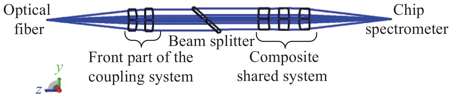
芯片式光谱仪入射光束耦合与对准监测系统结构如图1所示,系统由耦合前部分系统、监测后部分系统和复合共用系统三部分组成,复合共用系统需要同时配合耦合前部分系统与监测后部分系统分别完成光束耦合与耦合效果监测的功能,成功解决了监测系统的遮挡问题。即耦合前部分系统与复合共用系统构成了耦合系统,监测后部分系统与复合共用系统构成了监测系统。所设计的监测后部分系统与耦合系统为非共轴光学系统,不影响耦合系统工作,可在实现光斑与光谱仪对准后去除监测后部分系统,实现监测后部分系统共用。

Figure 1. Sketch of system for incident beam coupling and alignment monitoring of chip spectrometer
由于芯片式光谱仪接收端为光栅结构,在接收光束的同时存在反射,且光栅耦合需满足布拉格条件:当入射光矢量与光栅矢量叠加后的矢量方向刚好和波导的某一模式的传输方向上的分量相等时,可以通过光栅耦合进入波导中,因此将耦合系统倾斜一定角度提高耦合效率,并避免光在光栅结构上反射回发射端。耦合系统将光纤发出的光束以最大效率导入到芯片上,为了降低由于对准产生的能量损耗,要求经耦合系统在芯片式光谱仪上成像尺寸至少小于芯片式光谱仪接收端的尺寸,这里取接收端的一半。监测系统将芯片接收端放大成像在探测器上,利用分光装置同时实现反射和透射。
-
耦合系统满足拉赫不变量:
式中:n为物方介质折射率;y为物高;u为物方孔径角;n′为像方介质折射率;y′为像高;u′为像方孔径角;β为垂轴放大率。即光学系统在近轴区内成像时,在一对共轭平面内,物高y、孔径角u和介质折射率n的乘积为一常数。y′和u′是两个成反比例关系的量,增大像高,必然减小像方孔径角。耦合系统要求在芯片接收范围内光斑较大以便进行对准,且像方孔径角较大以便后方监测系统提高放大倍率,综合考虑取β=−1×左右[13]。
考虑到要与监测系统进行拼接,耦合系统与监测系统共用光路。因此先将光纤发出的光束准直,便于设置分光板对平行光进行透射与反射。后接复合共用系统对光线汇聚,成像在芯片的接收端面上。如此复合共用系统可同时配合耦合前部分系统与监测后部分系统分别完成光束耦合与耦合效果监测的功能。
-
由于复合共用系统需要同时配合耦合前部分系统与监测后部分系统分别完成光束耦合与耦合效果监测的功能,因此耦合系统的像面与监测系统的物面共面,耦合系统的像方孔径角即为监测系统的物方孔径角,但是成像在芯片接收端时要求光斑小于接收端面,监测时要求可以观察到整个接收端面,因此监测系统的物面要比耦合系统的像面大。监测系统需要将芯片接收端放大成像在探测器上以观察光束耦合情况,由于耦合系统需留出较大的后截距来更换芯片式光谱仪及调整接收端位置,即监测系统物距l较大,根据公式(2)可知,β值越大,像距l′越大,因此可以设置较低的放大倍率来降低系统的总长,现有的近红外探测器像元大小基本在25 μm×25 μm以内,因此设置β=−3×即可以使探测器分辨芯片式光谱仪的对准情况。通过复合共用系统将芯片式光谱仪的光线准直,再通过监测后部分系统成像在探测器上。
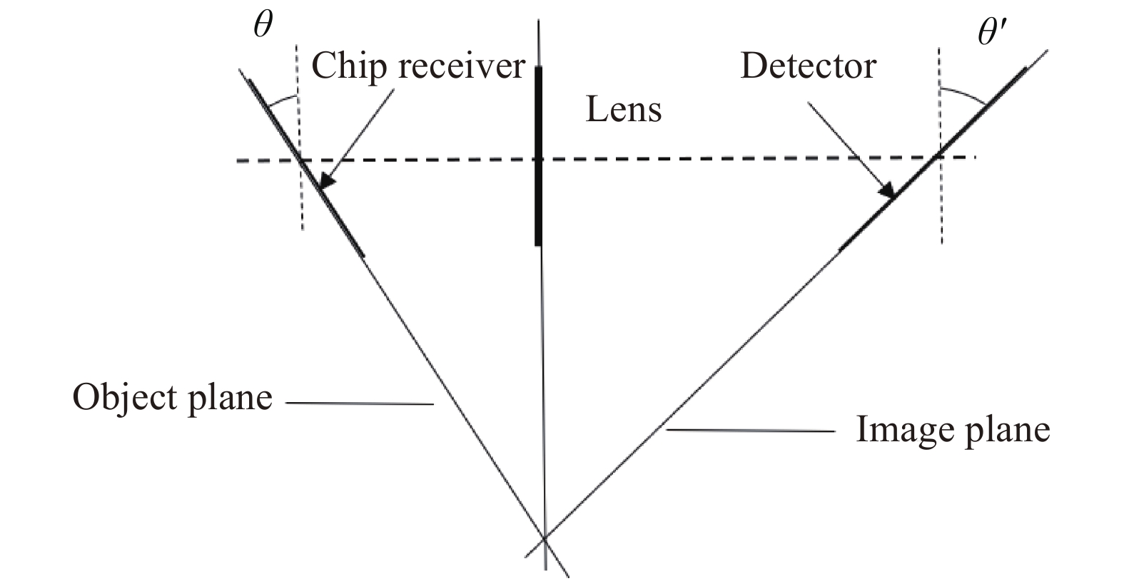
由于芯片式光谱仪接收端为光栅耦合器,而光栅耦合需满足布拉格条件,因此需耦合系统整体倾斜一定角度,监测系统与耦合系统共用一部分光路,则监测系统物面与光轴不垂直。根据Scheimpflug条件:
式中:β为放大倍率,物面、透镜主平面和像面延长线交于一点,设置像面倾斜来校正,如图2所示[14]。

Figure 2. Set the image plane tilt according to the Scheimpflug condition
-
本系统的指标参数如表1所示。
Parameter Data source Spectral range/nm 1 550±50 Fiber NA 0.12 Fiber diameter/μm 6 Chip receiving area/μm2 20×20 Angle between the optical axis and the chip normal/(°) 7 Coupling system vertical axis magnification −1× Monitoring system vertical axis magnification −3× Table 1. Optical design parameters
-
表2为耦合系统透镜数据,图3为耦合系统结构图,光纤光束通过耦合系统高效的耦合到芯片式光谱仪上。左侧为输入光纤,右侧为芯片接收端,前两片透镜为耦合前部分系统,后三片透镜为复合共用系统。
Lens Material Radius Radius Thickness Diameter 1 H−K9L −15.214 −5.546 0.800 2.536 2 H−K9L 64.029 −11.388 0.800 2.706 Beam splitter H−K9L Infinity Infinity 0.500 3.748 3 H−ZK3 13.385 6.184 1.000 2.326 4 H−K9L 22.000 −10.332 1.000 2.364 5 H−ZK3 5.400 30.545 1.000 2.278 Table 2. Coupling system lens data

Figure 3. Coupling system structure
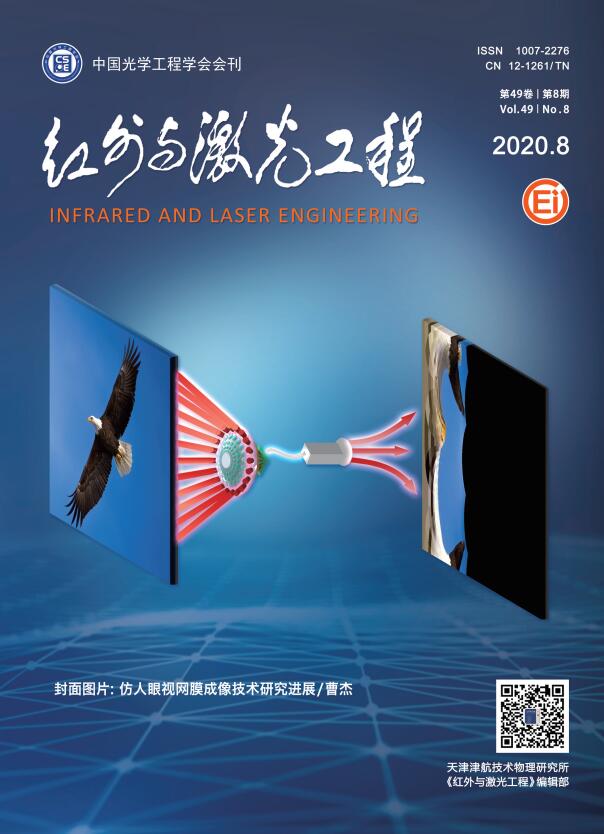
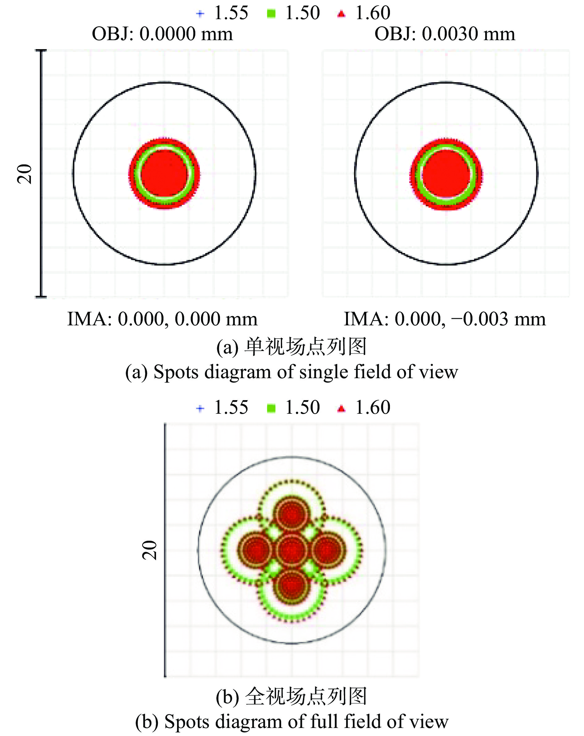
图4(a)、(b)为耦合系统的点列图,表明耦合系统在不同波长和视场下点列斑分布均匀,单个弥散斑半径在3 μm内,全视场光斑直径大小在12 μm内,小于集成芯片式光谱仪接收端尺寸。因此集成芯片式光谱仪接收端可接收到光纤发出的全部光束,避免能量浪费。
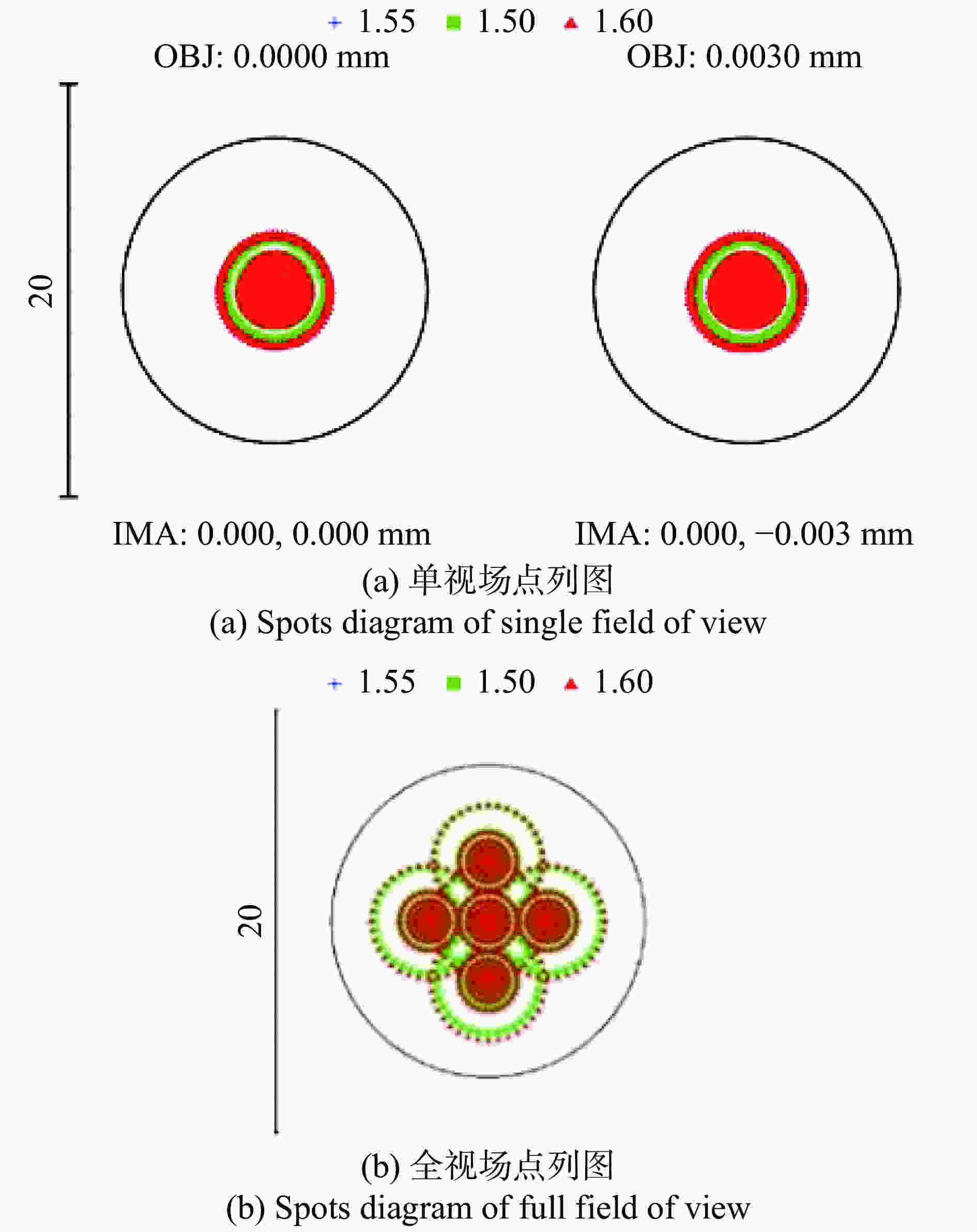
Figure 4. Schematic diagram of increase the distance between the fiber and the spectrometer
-
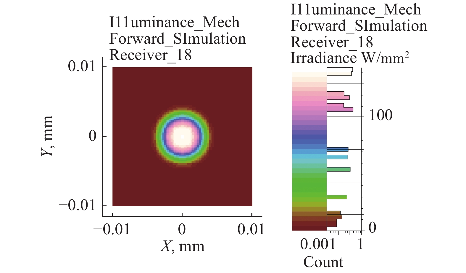
将耦合系统导入LightTools中进行能量分析,图5 为耦合系统能量图,可见能量集中在光栅耦合器中央位置且分布均匀。光源发出的总功率为0.005 665 7 W,通过LightTools模拟可得接收端总功率为0.004 153 3,则在光栅面处耦合效率为0.733。
Figure 5. Coupling system energy diagram
通过LightTools模拟及计算,可知光束耦合系统达到满足测试需求的耦合效率。
-
表3为耦合系统透镜数据,图6为监测系统结构图,底端为芯片接收端,左侧为探测器,下端为复合共用系统,上端为监测后部分系统。由于物面与光轴成7°倾斜角,通过公式计算得出像面倾斜角度,如图6所示。
Lens Material Radius Radius Thickness Diameter 1 H-ZK3 30.545 5.400 1.000 2.278 2 H-K9L −10.332 22.000 1.000 2.364 3 H-ZK3 6.184 13.385 1.000 2.326 4 H-ZK3 −7.211 −20.437 1.000 2.336 5 H-K9L 20.708 −30.453 1.000 2.178 6 H-K9L 65.430 15.977 1.000 2.090 Table 3. Monitoring system lens data

Figure 6. Monitoring system structure
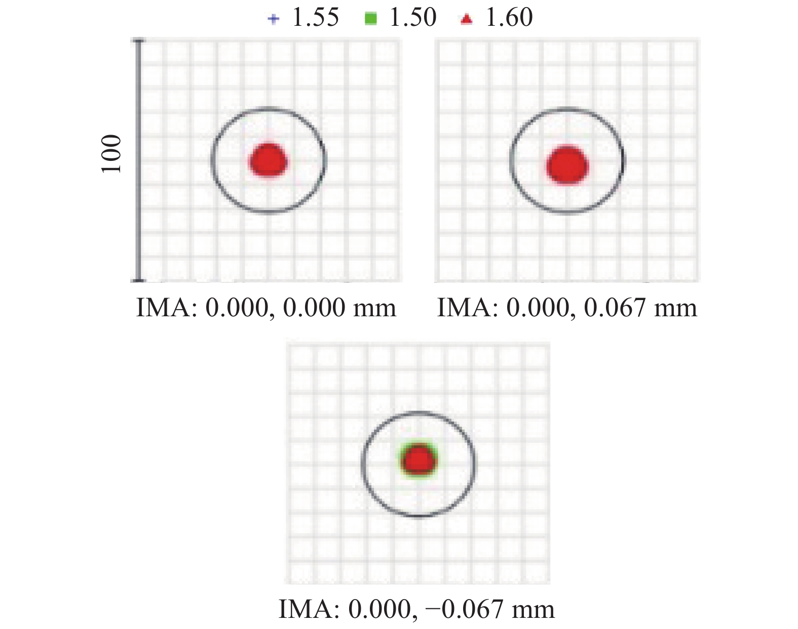
图7和图8为监测系统的点列图和MTF曲线,表明监测系统在不同波长和视场下点列斑均小于一个像元大小,MTF曲线均贴近衍射极限,成像效果良好,可通过监测系统清晰地观测到芯片式光谱仪接收端情况。
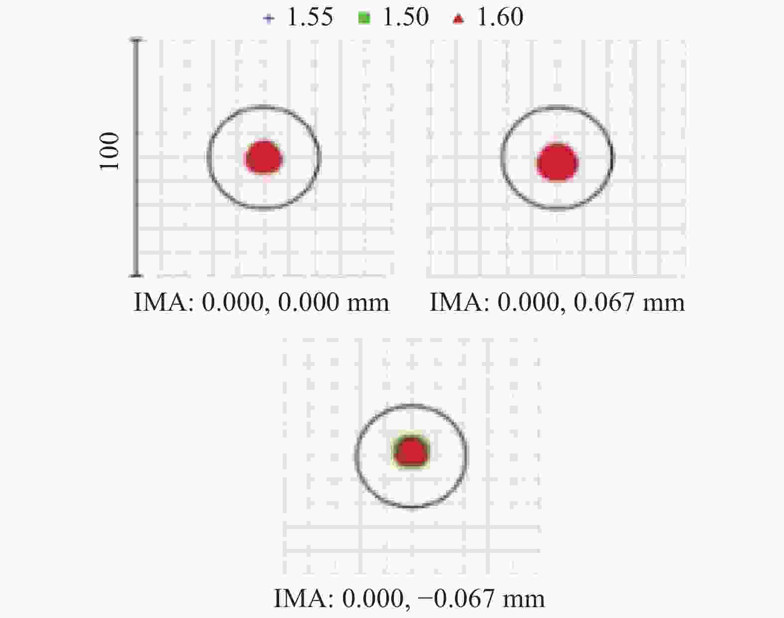
Figure 7. Spots diagram of different wavelengths and fields of views
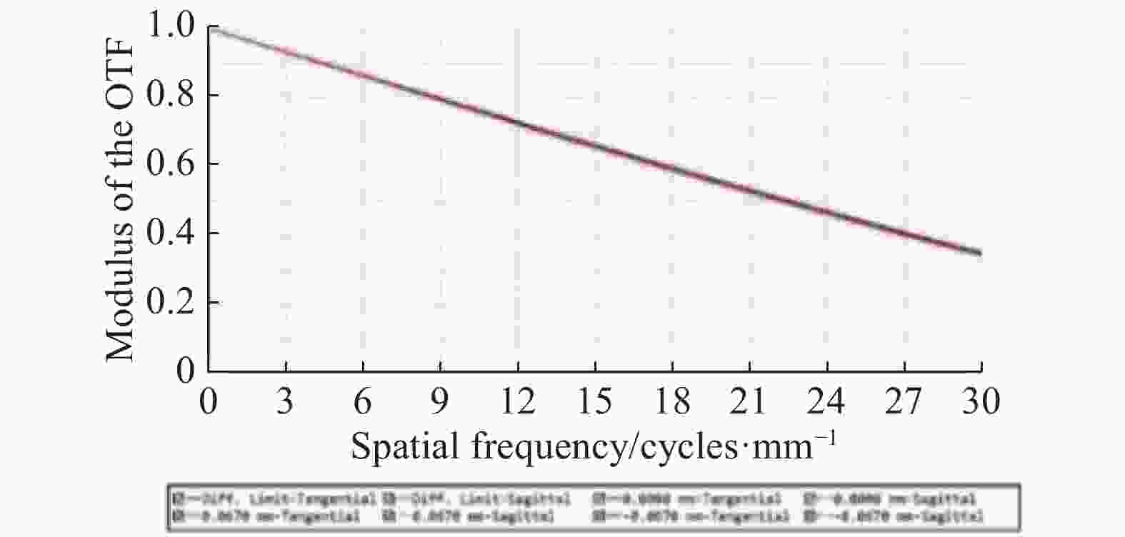
Figure 8. MTF of monitoring system
-
将设计优化的子系统进行拼接,完成最终的芯片式光谱仪入射光束耦合与对准监测系统的设计,如图9所示。系统用于芯片式光谱仪入射光的耦合时,可将光纤光束完整的成像在芯片接收端面上,提高能量的利用率;同时将光纤与芯片分离,解决了光纤与芯片的磨损问题;确定好芯片位置后添加一个卡槽,同尺寸同类型的芯片无需再次调整校准即可进行耦合;无需六维调节架来进行反复校准,提高效率的同时大大缩减了成本。且由于芯片式光谱仪入射光束耦合与对准监测系统设计了复合共用系统,因此可同时对芯片式光谱仪入射光的耦合效果进行实时监测,将耦合效果清晰的成像在探测器上。系统结构简单,易于固定,无需手动调节。
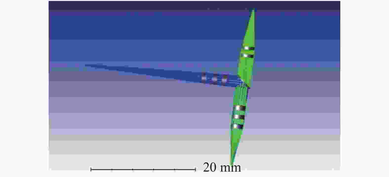
Figure 9. Structure of integrated optical system for incident beam coupling and alignment monitoring of chip spectrometer
-
文中设计的芯片式光谱仪入射光束耦合与对准监测集成光学系统结构简单,像质良好。此芯片式光谱仪入射光束耦合与对准监测集成光学系统解决了芯片式光谱仪的耦合及监测难的问题,提高能量利用率,实现了光纤与芯片式光谱仪的分离,可在光束的耦合的同时对耦合效果进行实时监测,为同类型的芯片式光谱仪的耦合与监测提供了参考,具有一定现实意义。
System design for beam coupling and alignment monitoring of chip spectrometer
doi: 10.3788/IRLA20190532
- Received Date: 2019-12-05
- Rev Recd Date: 2020-02-15
- Available Online: 2020-09-22
- Publish Date: 2020-08-28
-
Key words:
- chip spectrometer /
- beam coupling /
- composite shared optical path /
- alignment monitoring
Abstract: Aiming at the problem of the beam coupling and alignment monitoring of the chip spectrometer, an integrated optical system was proposed for avoiding the wear of the receiving end at chip spectrometer and the shielding of the optical fiber. The system consisted of a front coupling system, a rear monitor system and a composite sharing system. The composite sharing system needed to cooperate with the front coupling system and the rear monitor system to complete the beam coupling and alignment monitoring functions respectively. The final system was designed by multiple combinations, a coupling system and a monitoring system were designed for a 6 μm incident fiber and a 20 μm×20 μm chip spectrometer receiving end at (1 550±50) nm. The energy analysis of the coupled system was performed by LightTools. The coupling efficiency was 0.733. The final system has a simple structure and can perform beam coupling and alignment monitoring at the same time, which provides a new method for the beam coupling and monitoring of chip spectrometers.


 DownLoad: