Volume 49 Issue 9
Sep.  2020
Turn off MathJax
Article Contents

Guo Xuyue, Li Bingjie, Fan Xinhao, Zhong Jinzhan, Liu Sheng, Wei Bingyan, Li Peng, Zhao Jianlin. Complex amplitude modulation of light fields based on dielectric metasurfaces and its applications[J]. Infrared and Laser Engineering, 2020, 49(9): 20201031. doi: 10.3788/IRLA20201031
Citation: Guo Xuyue, Li Bingjie, Fan Xinhao, Zhong Jinzhan, Liu Sheng, Wei Bingyan, Li Peng, Zhao Jianlin. Complex amplitude modulation of light fields based on dielectric metasurfaces and its applications[J]. Infrared and Laser Engineering, 2020, 49(9): 20201031. doi: 10.3788/IRLA20201031

Complex amplitude modulation of light fields based on dielectric metasurfaces and its applications

doi: 10.3788/IRLA20201031
  • Received Date: 2020-06-11
  • Rev Recd Date: 2020-08-07
  • Available Online: 2020-09-22
  • Publish Date: 2020-09-22
  • Metasurface is an artificially ultrathin material with two-dimensional nanostructure array, which can achieve flexible modulation on amplitude, phase and polarization of light field in a sub-wavelength scale, providing a new possibility for the miniaturization and integration of modern optical devices. With the development of optical imaging, display and so on, the requirement of miniaturized optical devices with high efficiency in visible light band is becoming conspicuous. In recent years, optical metasurfaces fabricated by dielectric materials with high refractive indices and low losses have been extensively studied, showing application prospects in achromatic metalens, polarization-dependent holographic display, et al. Around the research on the metasurface of dielectric, firstly, the generalized Snell's law and the modulation principle of nanostructures in dielectric metasurface on amplitude, phase and polarization of light field were introduced. Then the research progress of dielectric metasurfaces in holographic display and structural light field generation, based on single- and multi-parameters modulation of light field was reviewed. At last, the possible challenges and prospects of dielectric metasurfaces were discussed.
  • [1] Veldkamp W B, McHugh T J. Binary optics [J]. Scientific American, 1992, 266(5): 92-97. doi:  10.1038/scientificamerican0592-92
    [2] Cai W, Shalaev V M. Optical Metamaterials[M]. USA: Springer, 2010.
    [3] Liu Y M, Zhang X. Metamaterials: A new frontier of science and technology [J]. Chemical Society Reviews, 2011, 40(5): 2494-2507. doi:  10.1039/c0cs00184h
    [4] Smith D R, Padilla W J, Vier D C, et al. Composite medium with simultaneously negative permeability and permittivity [J]. Physical Review Letters, 2000, 84(18): 4184-4187. doi:  10.1103/PhysRevLett.84.4184
    [5] Shelby R A, Smith D R, Schultz S. Experimental verification of a negative index of refraction [J]. Science, 2001, 292(5514): 77-79. doi:  10.1126/science.1058847
    [6] Cai W, Chettiar U K, Kildishev A V, et al. Optical cloaking with metamaterials [J]. Nature Photonics, 2007, 1(4): 224-227. doi:  10.1038/nphoton.2007.28
    [7] Schurig D, Mock J J, Justice B J, et al. Metamaterial electromagnetic cloak at microwave frequencies [J]. Science, 2006, 314(5801): 977-980. doi:  10.1126/science.1133628
    [8] Pendry J B. Negative refraction makes a perfect lens [J]. Physical Review Letters, 2000, 85(18): 3966-3969. doi:  10.1103/PhysRevLett.85.3966
    [9] Yu N F, Genevet P, Kats M A, et al. Light propagation with phase discontinuities: Generalized laws of reflection and refraction [J]. Science, 2011, 334(6054): 333-337. doi:  10.1126/science.1210713
    [10] Chen S Q, Li Z C, Liu W W, et al. From single-dimensional to multidimensional manipulation of optical waves with metasurfaces [J]. Advanced Materials, 2019, 31(16): 1802458. doi:  10.1002/adma.201802458
    [11] Chen S Q, Liu W W, Li Z C, et al. Metasurface-empowered optical multiplexing and multifunction [J]. Advanced Materials, 2020, 32(3): 1805912. doi:  10.1002/adma.201805912
    [12] Li Z C, Liu W W, Cheng H, et al. Spin-selective full-dimensional manipulation of optical waves with chiral mirror [J]. Advanced Materials, 2020, 32(26): 1907983. doi:  10.1002/adma.201907983
    [13] Liu W W, Cheng H, Tian J G, et al. Diffractive metalens: From fundamentals, practical applications to current trends [J]. Advances in Physics: X, 2020, 5(1): 1742584. doi:  10.1080/23746149.2020.1742584
    [14] Deng Z L, Deng J H, Zhuang X, et al. Diatomic metasurface for vectorial holography [J]. Nano Letters, 2018, 18(5): 2885-2892. doi:  10.1021/acs.nanolett.8b00047
    [15] Wen D D, Yue F Y, Li G X, et al. Helicity multiplexed broadband metasurface holograms [J]. Nature Communications, 2015, 6: 8241. doi:  10.1038/ncomms9241
    [16] Arbabi A, Horie Y, Bagheri M, et al. Dielectric metasurfaces for complete control of phase and polarization with subwavelength spatial resolution and high transmission [J]. Nature Nanotechnology, 2015, 10(11): 937-943. doi:  10.1038/nnano.2015.186
    [17] Mueller J B, Rubin N A, Devlin R C, et al. Metasurface polarization optics: independent phase control of arbitrary orthogonal states of polarization [J]. Physical Review Letters, 2017, 118(11): 113901. doi:  10.1103/PhysRevLett.118.113901
    [18] Aieta F, Genevet P, Kats M A, et al. Aberration-free ultrathin flat lenses and axicons at telecom wavelengths based on plasmonic metasurfaces [J]. Nano Letters, 2012, 12(9): 4932-4936. doi:  10.1021/nl302516v
    [19] Yu N F, Aieta F, Genevet P, et al. A broadband, background-free quarter-wave plate based on plasmonic metasurfaces [J]. Nano Letters, 2012, 12(12): 6328-6333. doi:  10.1021/nl303445u
    [20] Sun S L, He Q, Xiao S Y, et al. Gradient-index meta-surfaces as a bridge linking propagating waves and surface waves [J]. Nature Materials, 2012, 11(5): 426-431. doi:  10.1038/nmat3292
    [21] Chen C, Song W G, Chen J W, et al. Spectral tomographic imaging with aplanatic metalens [J]. Light-Science & Applications, 2019, 8(6): 990-997. doi:  10.1038/s41377-019-0208-0
    [22] Wang S M, Wu P C, Su V C, et al. Broadband achromatic optical metasurface devices [J]. Nature Communications, 2017, 8(1): 187. doi:  10.1038/s41467-017-00166-7
    [23] Lin R J, Su V C, Wang S M, et al. Achromatic metalens array for full-colour light-field imaging [J]. Nature Nanotechnology, 2019, 14(3): 227-231. doi:  10.1038/s41565-018-0347-0
    [24] Pu M, Li X, Ma X, et al. Catenary optics for achromatic generation of perfect optical angular momentum [J]. Science Advances, 2015, 1(9): 1-7. doi:  10.1126/sciadv.1500396
    [25] Cheng H, Liu Z C, Chen S Q, et al. Emergent functionality and controllability in few-layer metasurfaces [J]. Advanced Materials, 2015, 27(36): 5410-5421. doi:  10.1002/adma.201501506
    [26] Liu Z C, Li Z C, Liu Z, et al. High-performance broadband circularly polarized beam deflector by mirror effect of multinanorod metasurfaces [J]. Advanced Functional Materials, 2015, 25(34): 5428-5434. doi:  10.1002/adfm.201502046
    [27] Zheng G X, Mühlenbernd H, Kenney M, et al. Metasurface holograms reaching 80% efficiency [J]. Nature Nanotechnology, 2015, 10(4): 308-312. doi:  10.1038/nnano.2015.2
    [28] Yang Y M, Wang W Y, Moitra P, et al. Dielectric meta-reflectarray for broadband linear polarization conversion and optical vortex generation [J]. Nano Letters, 2014, 14(3): 1394-1399. doi:  10.1021/nl4044482
    [29] Lin Dianmin, Fan Pengyu, Erez Hasman, et al. Dielectric gradient metasurface optical elements [J]. Science, 2014, 345(6194): 298-302. doi:  10.1126/science.1253213
    [30] Kamali S M, Arbabi E, Arbabi A, et al. A review of dielectric optical metasurfaces for wavefront control [J]. Nanophotonics, 2018, 7(6): 1041-1068. doi:  10.1515/nanoph-2017-0129
    [31] Zhang F, Pu M B, Li X, et al. All‐dielectric metasurfaces for simultaneous giant circular asymmetric transmission and wavefront shaping based on asymmetric photonic spin–orbit interactions [J]. Advanced Functional Materials, 2017, 27(47): 1704295. doi:  10.1002/adfm.201704295
    [32] Liu W W, Li Z C, Li Z, et al. Energy‐tailorable spin‐selective multifunctional metasurfaces with full fourier components [J]. Advanced Materials, 2019, 31(32): 1901729.
    [33] Li S Q, Li X Y, Wang G X, et al. Multidimensional manipulation of photonic spin hall effect with a single‐layer dielectric metasurface [J]. Advanced Optical Materials, 2019, 7(5): 1801365. doi:  10.1002/adom.201801365
    [34] Feng H, Li Q T, Wan W P, et al. Spin-switched three-dimensional full-color scenes based on a dielectric meta-hologram [J]. ACS Photonics, 2019, 6(11): 2910-2916. doi:  10.1021/acsphotonics.9b01017
    [35] Fan Q B, Zhu W Q, Liang Y Z, et al. Broadband generation of photonic spin-controlled arbitrary accelerating light beams in the visible [J]. Nano Letters, 2019, 19(2): 1158-1165. doi:  10.1021/acs.nanolett.8b04571
    [36] Jin L, Dong Z G, Mei S T, et al. Noninterleaved Metasurface for (26-1) Spin-and Wavelength-Encoded Holograms [J]. Nano Letters, 2018, 18(12): 8016-8024.
    [37] Huang K, Deng J, Leong H S, et al. Ultraviolet metasurfaces of ≈80% efficiency with antiferromagnetic resonances for optical vectorial anti-counterfeiting [J]. Laser & Photonics Reviews, 2019, 13(5): 1800289. doi:  10.1002/lpor.201800289
    [38] Zhang C, Divitt S, Fan Q B, et al. Low-loss metasurface optics down to the deep ultraviolet region [J]. Light-Science & Applications, 2020, 9(1): 1-10. doi:  10.1038/s41377-020-0287-y
    [39] Yu N F, Capasso F. Flat optics with designer metasurfaces [J]. Nature Materials, 2014, 13(2): 139-150. doi:  10.1038/nmat3839
    [40] Lalanne P, Morris G M. Antireflection behavior of silicon subwavelength periodic structures for visible light [J]. Nanotechnology, 1997, 8(2): 53-56. doi:  10.1088/0957-4484/8/2/002
    [41] Bomzon Z, Biener G, Kleiner V, et al. Radially and azimuthally polarized beams generated by space-variant dielectric subwavelength gratings [J]. Optics Letters, 2002, 27(5): 285-287. doi:  10.1364/OL.27.000285
    [42] Lalanne P, Astilean S, Chavel P, et al. Blazed binary subwavelength gratings with efficiencies larger than those of conventional échelette gratings [J]. Optics Letters, 1998, 23(14): 1081-1083. doi:  10.1364/OL.23.001081
    [43] Khorasaninejad M, Capasso F. Metalenses: Versatile multifunctional photonic components [J]. Science, 2017, 358(6367): 1-8. doi:  10.1126/science.aam8100
    [44] Kuznetsov A I, Miroshnichenko A E, Brongersma M L, et al. Optically resonant dielectric nanostructures [J]. Science, 2016, 354(6314): 1-8. doi:  10.1126/science.aag2472
    [45] Wang L, Kruk S, Tang H Z, et al. Grayscale transparent metasurface holograms [J]. Optica, 2016, 3(12): 1504-1505. doi:  10.1364/OPTICA.3.001504
    [46] Devlin R C, Khorasaninejad M, Chen W T, et al. Broadband high-efficiency dielectric metasurfaces for the visible spectrum [J]. Proceedings of the National Academy of Sciences of the United States of America, 2016, 113(38): 10473-10478. doi:  10.1073/pnas.1611740113
    [47] Guo X Y, Li P, Li B J, et al. Visible-frequency broadband dielectric metahologram by random Fourier phase-only encoding [J]. Science China Physics, Mechanics & Astronomy, 2021, 64(1): 214211.
    [48] Li J X, Chen S Q, Yang H F, et al. Metasurfaces: Simultaneous control of light polarization and phase distributions using plasmonic metasurfaces [J]. Advanced Functional Materials, 2015, 25(5): 704-710. doi:  10.1002/adfm.201570036
    [49] Yin X B, Ye Z L, Rho J, et al. Photonic spin hall effect at metasurfaces [J]. Science, 2013, 339(6126): 1405-1407. doi:  10.1126/science.1231758
    [50] Clark T W, Offer R F, Franke-Arnold S, et al. Comparison of beam generation techniques using a phase only spatial light modulator [J]. Optics Express, 2016, 24(6): 6249-6264. doi:  10.1364/OE.24.006249
    [51] Jiang Q, Jin G F, Cao L C. When metasurface meets hologram: principle and advances [J]. Advances in Optics and Photonics, 2019, 11(3): 518-576. doi:  10.1364/AOP.11.000518
    [52] Huang K, Dong Z G, Mei S T, et al. Silicon multi‐meta‐holograms for the broadband visible light [J]. Laser & Photonics Reviews, 2016, 10(3): 500-509. doi:  10.1002/lpor.201500314
    [53] Zhao W Y, Jiang H, Liu B Y, et al. Dielectric Huygens’ metasurface for high-efficiency hologram operating in transmission mode [J]. Scientific Reports, 2016, 6: 30613. doi:  10.1038/srep30613
    [54] Yoon G, Lee D, Nam K T, et al. Pragmatic metasurface hologram at visible wavelength: The balance between diffraction efficiency and fabrication compatibility [J]. ACS Photonics, 2018, 5(5): 1643-1647. doi:  10.1021/acsphotonics.7b01044
    [55] Wang B, Dong F L, Li Q T, et al. Visible-frequency dielectric metasurfaces for multiwavelength achromatic and highly dispersive holograms [J]. Nano Letters, 2016, 16(8): 5235-5240. doi:  10.1021/acs.nanolett.6b02326
    [56] Cooley J W, Tukey J W. An algorithm for the machine calculation of complex Fourier series [J]. Mathematics of Computation, 1965, 19(90): 297-301. doi:  10.1090/S0025-5718-1965-0178586-1
    [57] Gerchberg R W. A practical algorithm for the determination of phase from image and diffraction plane pictures [J]. Optik, 1972, 35: 237-246.
    [58] Davis J A, Cottrell D M, Campos J, et al. Encoding amplitude information onto phase-only filters [J]. Applied Optics, 1999, 38(23): 5004-5013. doi:  10.1364/AO.38.005004
    [59] Mendoza-Yero O, Mínguez-Vega G, Lancis J. Encoding complex fields by using a phase-only optical element [J]. Optics Letters, 2014, 39(7): 1740-1743. doi:  10.1364/OL.39.001740
    [60] Guo X Y, Zhong J Z, Li P, et al. Creation of topological vortices using Pancharatnam-Berry phase liquid crystal holographic plates [J]. Chinese Physics B, 2020, 29(4): 102-106.
    [61] Devlin R C, Ambrosio A, Rubin N A, et al. Arbitrary spin-to–orbital angular momentum conversion of light [J]. Science, 2017, 358(6365): 896-901. doi:  10.1126/science.aao5392
    [62] Dutton Z, Ruostekoski J. Transfer and storage of vortex states in light and matter waves [J]. Physical Review Letters, 2004, 93(19): 193602. doi:  10.1103/PhysRevLett.93.193602
    [63] Ruostekoski J, Anglin J R. Creating vortex rings and three-dimensional skyrmions in Bose-Einstein condensates [J]. Physical Review Letters, 2001, 86(18): 3934. doi:  10.1103/PhysRevLett.86.3934
    [64] Guo X, Li P, Zhong J, et al. Tying polarization-switchable optical vortex knots and links via holographic all-dielectric metasurfaces [J]. Laser & Photonics Reviews, 2020, 14(3): 1900366.
    [65] Zhong J Z, Qi S X, Liu S, et al. Accurate and rapid measurement of optical vortex links and knots [J]. Optics Letters, 2019, 44(15): 3849-3852. doi:  10.1364/OL.44.003849
    [66] Wang L, Zhang W X, Yin H X, et al. Ultrasmall optical vortex knots generated by spin-selective metasurface holograms [J]. Advanced Optical Materials, 2019, 7(10): 1900263. doi:  10.1002/adom.201900263
    [67] Leach J, Dennis M R, Courtial J, et al. Vortex knots in light [J]. New Journal of Physics, 2005, 7(1): 55. doi:  10.1088/1367-2630/7/1/055
    [68] Overvig A C, Shrestha S, Malek S C, et al. Dielectric metasurfaces for complete and independent control of the optical amplitude and phase [J]. Light-Science & Applications, 2019, 8(5): 860-871. doi:  10.1038/s41377-019-0201-7
    [69] Lee G Y, Yoon G, Lee S Y, et al. Complete amplitude and phase control of light using broadband holographic metasurfaces [J]. Nanoscale, 2018, 10(9): 4237-4245.
    [70] Fan X, Li P, Guo X, et al. Axially tailored light field by means of a dielectric metalens [J]. Physical Review Applied, 2020, 14(2): 024035.
    [71] Li S Q, Xu X W, Veetil R M, et al. Phase-only transmissive spatial light modulator based on tunable dielectric metasurface [J]. Science, 2019, 364(6445): 1087-1090. doi:  10.1126/science.aaw6747
    [72] Li J X, Yu P, Cheng H, et al. Optical polarization encoding using graphene-loaded plasmonic metasurfaces [J]. Advanced Optical Materials, 2016, 4(1): 91-98. doi:  10.1002/adom.201500398
    [73] Qu Y R, Li Q, Du K K, et al. Dynamic thermal emission control based on ultrathin plasmonic metamaterials including phase-changing material GST [J]. Laser & Photonics Reviews, 2017, 11(5): 1700091. doi:  10.1002/lpor.201700091
  • 加载中
通讯作者: 陈斌, bchen63@163.com
  • 1. 

    沈阳化工大学材料科学与工程学院 沈阳 110142

  1. 本站搜索
  2. 百度学术搜索
  3. 万方数据库搜索
  4. CNKI搜索

Figures(6)

Article Metrics

Article views(1121) PDF downloads(247) Cited by()

Related
Proportional views

Complex amplitude modulation of light fields based on dielectric metasurfaces and its applications

doi: 10.3788/IRLA20201031
  • Shaanxi Key Laboratory of Optical Information Technology, School of Physical Science and Technology, Northwestern Polytechnical University, Xi’an 710129, China

Abstract: Metasurface is an artificially ultrathin material with two-dimensional nanostructure array, which can achieve flexible modulation on amplitude, phase and polarization of light field in a sub-wavelength scale, providing a new possibility for the miniaturization and integration of modern optical devices. With the development of optical imaging, display and so on, the requirement of miniaturized optical devices with high efficiency in visible light band is becoming conspicuous. In recent years, optical metasurfaces fabricated by dielectric materials with high refractive indices and low losses have been extensively studied, showing application prospects in achromatic metalens, polarization-dependent holographic display, et al. Around the research on the metasurface of dielectric, firstly, the generalized Snell's law and the modulation principle of nanostructures in dielectric metasurface on amplitude, phase and polarization of light field were introduced. Then the research progress of dielectric metasurfaces in holographic display and structural light field generation, based on single- and multi-parameters modulation of light field was reviewed. At last, the possible challenges and prospects of dielectric metasurfaces were discussed.

    • 振幅、相位及偏振是光波的基本特征参量,光学元件各种功能的实现依赖于对光场参量的有效调控。例如,传统的光学元件对光场相位的调控主要是基于光波的折/反射原理,即利用材料的折射率差异以及光学元件面形,通过光程的累积来实现特定的相位分布,从而实现光波的聚焦、成像、分束等功能。然而,受限于自然界光学材料的选择范围,传统的光学元件往往具有较大的体积和质量,并且通常只具有单一的功能。微电子加工技术的进步推动了光学技术的高速发展,20世纪末,麻省理工学院林肯实验室的Veldkamp研究组首次提出了基于光波衍射理论的“二元光学”概念[1]。二元光学元件是一类利用计算机辅助设计和超大规模集成电路制备工艺,在衬底或传统光学元件表面刻蚀出具有多个台阶深度浮雕结构的纯相位衍射光学元件。相比于传统的折、反射式光学元件,二元光学元件摒弃了冗余的2$\pi $相位,具有质量轻、成本低、易复制等优点,在一定程度上实现了光学器件的小型化、平面化。

      然而,二元光学元件受其调制原理以及材料特性的限制,不可避免地存在着视场小、色差大的缺点,并且在常用光波段,基于衍射原理的光学元件仍具有较大体积。为进一步减小光学元件的尺寸,需要探索新型的光场波前调控机制与方法。在此背景下,具有亚波长单元的人工结构材料——超材料[2-3]被提出。超材料是一种三维的人工复合材料,具有周期性的亚波长结构,通过合理的设计可以实现自然材料无法实现的电磁参数与电磁响应,提高并拓展了调控光场分布的灵活性和自由度,目前已经在负折射[4-5]、电磁隐身[6-7]、高分辨成像[8]等多个领域展现出巨大的应用潜力。然而,随着超材料结构单元尺寸的不断减小,工作波长也逐渐向高频段推进,体超材料逐渐显现出损耗大、难加工的缺点,严重阻碍了其进一步的应用。在上述问题的推动下,具有亚波长厚度的超材料——超表面应运而生。2011年,哈佛大学Capasso教授团队首次提出了超表面的概念,利用广义斯涅耳定律精确设计V型金属纳米天线,实现了在亚波长尺度上对光波相位的有效调控[9]。由此开启了利用超表面结构实现光场调控的新方向。

      独特的调控机理和灵活的设计方式使得超表面具有非常丰富的光场调控自由度,因此受到研究者们的广泛关注[10-17]。例如,Capasso教授团队在后续的工作中基于V型天线设计实现了平板透镜、锥棱镜和超表面四分之一波片[18-19];复旦大学周磊教授团队采用H型金属纳米结构实现了反射聚焦并利用相位梯度超表面实现了传输波向表面波的转化[20];南京大学祝世宁院士团队发展出宽带消色差的超表面设计方案,并先后在近红外和可见光波段实现了超宽带的消色差超透镜[21-23];此外,中国科学院光电技术研究所罗先刚院士以及南开大学陈树琪教授团队分别提出了悬链线结构[24]和少层超表面(Few-layer Metasurfaces)[25]概念,有效提高了超表面器件的工作效率和可操控性。随着微纳加工技术的进步以及超表面器件的逐渐实用化,在可见光波段具有高工作效率的微型光学器件的需求日益增长。在微纳光子学领域中,金属的欧姆损耗是限制器件性能的主要因素,而金属材料超表面调控效率的理论上限为25%[26]。因此早期的超表面多为“金属—电介质—金属”结构[27]的反射式超表面,通过金属薄膜和纳米结构之间光波的多次反射和干涉来增强纳米结构与光波的相互作用,从而提高超表面的调控效率。电介质超表面的出现[28]以及电介质材料在超表面中的逐渐应用[29-30],从根本上解决了超表面调控效率低的问题。相比于金属材料,电介质材料具有高折射率、低损耗的特点,在特定波段具有极高的透射率。此外,透射型的超表面在实际应用中会带来比金属反射型超表面更多的便利。近年来,基于电介质材料的光学超表面得到了极大地发展,在近红外[31-33]、可见光[34-36]以及紫外[37-38]波段均表现出优越的调制效果,并且在消色差超透镜、偏振相关全息显示等多个领域展现出广泛的应用前景。

      超表面结构能够在亚波长尺度下实现光场振幅、相位及偏振的有效调控,为开发平面化、小型化、集成化的光学器件与光学系统提供了全新的途径,也为拓展光在通信、数据存储、生物医学等领域的进一步应用创造了契机。文中将从广义斯涅耳定律及电介质超表面单元调控光场振幅、相位和偏振态的基本原理出发,系统介绍笔者所在团队在利用电介质超表面实现光场参量调控方面取得的最新研究进展,并展望超表面发展的可能方向。

    • 超表面起源于人们对斯涅耳定律的重新探索,其对光场参量的调控依赖于局部纳米结构对光波的响应。因此,超表面器件的设计关键在于根据所需的光学响应分布函数,通过研究纳米结构对光波的响应作用来确定结构参数,如组成材料、结构形状、结构参数变化范围等。最后,对离散的结构单元进行合理排布,阵列结构单元共同作用从而实现宏观的光场调控。

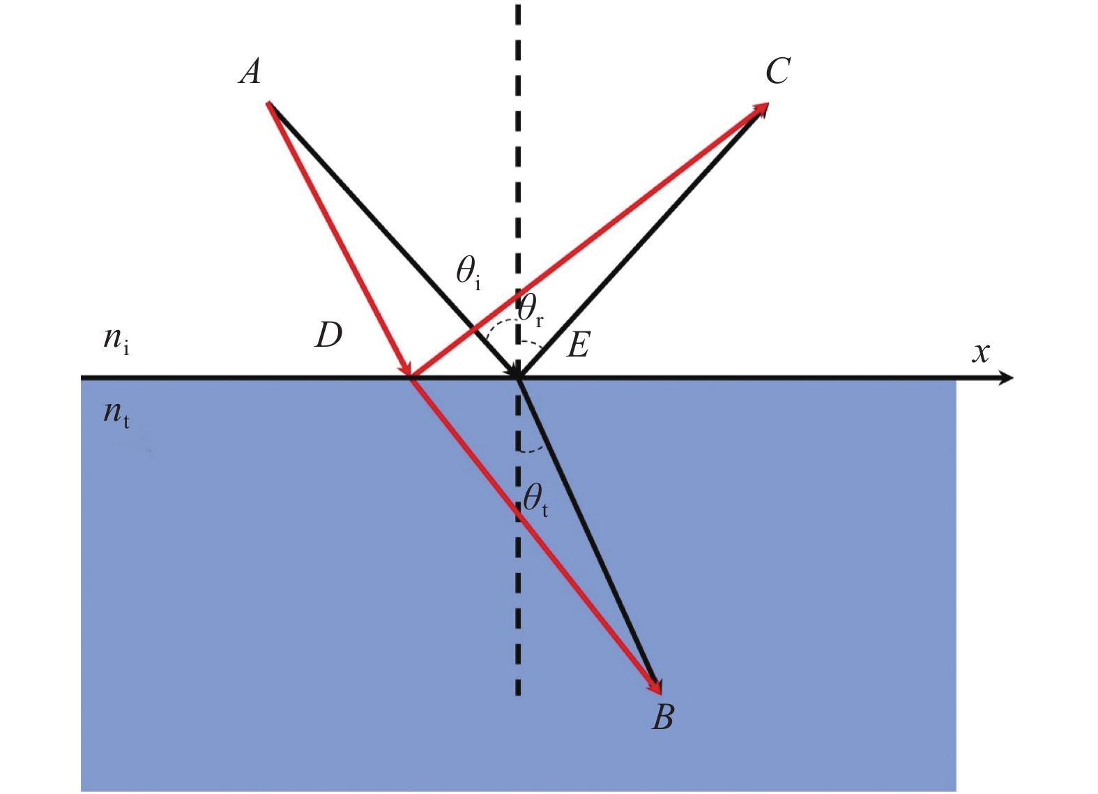
    • 费马原理表明,光传播的实际路径为光程取极值的路径,根据这一原理可以得到斯涅耳定律。但是,当两种介质的分界面存在相位突变ϕ时,斯涅耳定律则需要改写。如图1所示,相位突变量ϕx方向以一定梯度分布,从A点出发的光线经界面不同位置DE到达B点(折射)或C点(反射),光波通过两种折射路径(ADBAEB)和反射路径(ADCAEC)会获得相同的相移,表示为:

      Figure 1.  Generalized Snell's law[9, 39]

      式中:dx、dϕ分别为两种光路在界面处的距离及相位差;dϕ/dx为相位突变量的梯度,可以推导出如下广义斯涅耳定律[9, 39]

      可以看出,光波的折/反射行为与界面处引入的相位梯度相关,这为光波的调控提供了一个新的自由度。通过控制相位梯度dϕ/dx,可以实现光波折/反射行为的有效操纵。

    • 早在20世纪末21世纪初,硅、氧化钛等材料就被用于制备具有亚波长结构的光学元件[40-42]。直到2014年,范德堡大学Valentine教授团队[28]及斯坦福大学Brongersma教授团队[29]用电介质材料代替金属,通过硅纳米天线分别设计了反射式、透射式的超表面器件,使得器件的效率得以显著提升,自此激起了全电介质超表面的研究热潮。不同于金属超表面中利用金属结构的局域表面等离激元共振效应所实现的相位调控,电介质超表面通过高折射率电介质结构的等效波导效应[43]或米氏共振[44]实现相位调控。在光波段,由于硅、氧化钛等电介质材料能够与光波产生较强的相互作用且过程中几乎无损耗,因此电介质超表面具有极高的调控效率。例如,2016年,L.Wang等通过透射式硅基超表面实现了效率超过90%的全息成像[45]

      电介质超表面的效率在较大程度上取决于组成材料的光学性质,即复折射率(n' = n + iκ)。为确保2
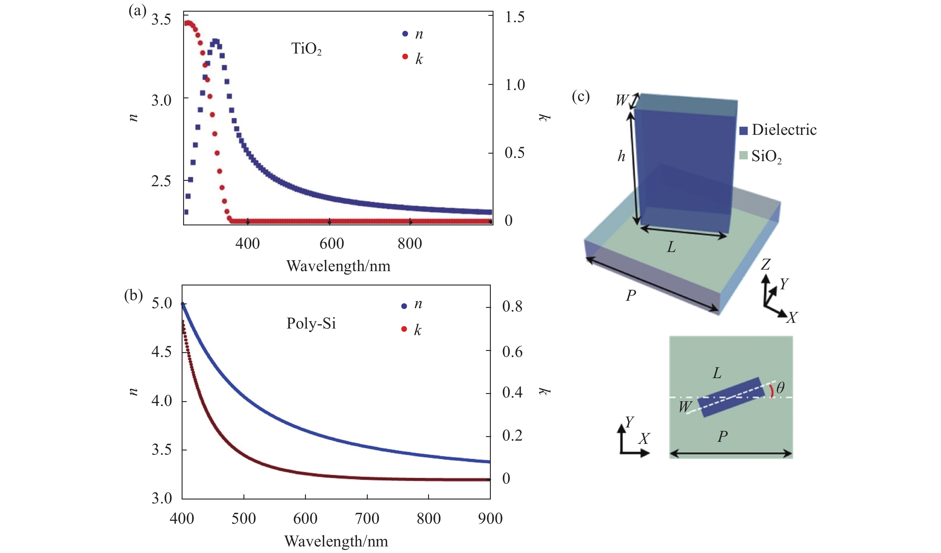
$\pi $的相位调制深度和较高的传输效率,材料应该具有较高的折射率(n > 2)和较低的吸收损耗(κ ≈ 0)。早期的电介质超表面受限于加工技术,主要以单晶硅、非晶硅为材料,工作波段集中在近红外波段。随着纳米加工技术的进步,研究工作逐渐向可见光波段推进,在高频段具有较高损耗的单晶硅已无法满足超表面的设计需求。因此氮化硅(Si3N4)、氧化钛(TiO2)、多晶硅(Polycrystalline Silicon, Poly–Si)等电介质材料先后被引入,这些材料能够在避免高损耗的同时提供优良的调控性能,现已广泛应用于电介质超表面的设计。图2(a)2(b)给出了氧化钛和多晶硅在可将光波段的复折射率[46-47]。可以看出,氧化钛和多晶硅在可见光波段均具有较高的折射率和较低的吸收损耗。此外,五氧化二铌(Nb2O5[37]、氧化铪(HfO2[38]等材料的引入使得超表面对光波的调制作用可以深入到紫外波段,极大地扩展了超表面的应用范围。

      Figure 2.  (a), (b) Complex refractive indices of TiO2 and Poly–Si in visible light band[46-47]; (c) Schematic illustration of a metasurface element with rectangle geometry

    • 电介质超表面对光波的调控原理可以采用等效波导效应和米氏共振效应解释。得益于电介质材料的高折射率特点,模场能够有效局域在单元结构中,因此邻近结构之间的耦合通常可以忽略不计,每一个结构都可以看作具有独立调制作用的“一块拼图”[48]

      采用等效波导效应分析其纳米结构单元的调制效应时,可将单元结构可等效为一个双折射元件。以常见的矩形单元结构为例,如图2(c)所示,该单元结构具有沿长、短边的对称轴(可视作双折射元件的快、慢轴),其对光波的调制作用可用沿这两个对称轴方向振动的特征分量的透射复振幅表示。假设沿快、慢轴的偏振分量的透射振幅分别为ToTe,相位延迟为φoφe,快轴与水平方向的夹角为θ。因此,单元结构的调制作用可用琼斯矩阵表示为:

      式中:R(θ)为旋转矩阵。假设光波在快、慢轴方向上具有相同的透射效率,即To=Te=T,引入相位延迟δ和传输相位φ0,即δ=φoφeφ0=(φo+φe)/2,则矩阵可改写为:

      对于一束圆偏振入射光[1 i]T,其透射场可表示为:

      上式表明,输出场包含两个正交圆偏振分量。第一个透射分量具有与入射光相同的偏振态,也称为共极化分量(co-polarized component);第二个透射分量具有与入射光相反的圆偏振态,因此也称为交叉极化分量(cross-polarized component),其复振幅表示为Tsin(δ/2)exp[i(φ0 + 2θ)]。由此可见,两个正交分量的振幅和相位与单元结构参量Tδφ0θ密切相关。例如,透射光中两个正交分量的占比取决于双折射单元结构的相位延迟δ,当δ = ±$\pi $时,单元结构等效于一个半波片,即cos(δ/2) = 0,sin(δ/2) = ±1。此时,入射光完全转换为交叉极化分量,共极化分量被完全消除。

      除了偏振调控作用,公式(5)反映了交叉极化分量和共极化分量的复振幅与结构参量Tδφ0θ均密切相关,这也为灵活调控两个分量的复振幅提供了充足的手段。如,对透过率T及相位延迟量δ的调控可实现任意的振幅调制;改变单元旋转角度θ和传输相位φ0,则可以分别实现几何相位(又称Pancharatnam-Berry相位)和传输相位的调制。基于上述原理,笔者围绕电介质超表面光场复振幅调控,在全息显示、结构光场产生等方面开展了相关研究。

    • 在光场调控研究中,相位一直以来都是研究的重点。通过对相位这一参量的调控即可实现多种功能器件,如波片、透镜,以及自旋相关的传输演化操控[49]等。光场的其它参量调控也可以借助相位调制实现。例如,基于振幅编码的纯相位调制技术[50]已成为实现光场振幅调控的有效途径,被广泛应用于超表面全息显示领域[51-53]

      在超表面全息显示中,设计原理与编码方法是影响最终成像效果的关键。基于传输相位的全息超表面可以实现偏振无关的全息显示,但其相位调制深度与波长相关[54]图3(a))。几何相位调制限定了圆偏振入射,但其相位调制作用与波长无关46图3(b)),并且选取窄波段响应的结构能够实现多波长彩色全息显示[55]图3(c))。另一方面,计算全息图(Computer-Generated Hologram, CGH)[56]的计算复杂度、成像清晰度、能量利用率等均与编码方法以及再现设备相关。然而传统的全息图编码方法均存在一定的弊端,如经典的GS算法[57]收敛速度慢,当迭代次数不够充分时,重建图像具有局部失真的情况,不能充分的显示重建图像的真实性。为此,基于光栅衍射的相位光栅法[58]和基于双相位低通滤波的棋盘法[59]先后被提出,这两种方法都可实现光场的复振幅重建,但代价是效率的降低和空间带宽的损失。

      Figure 3.  Holographic display realized by dielectric metasurfaces with (a) transmission phase[54] ; (b) Geometric phase[46] modulations; (c) Multi-wavelength color holographic display[55]

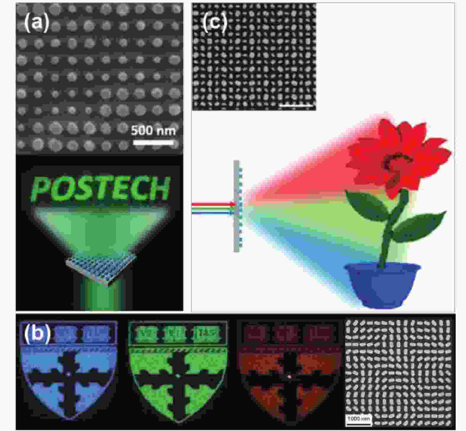
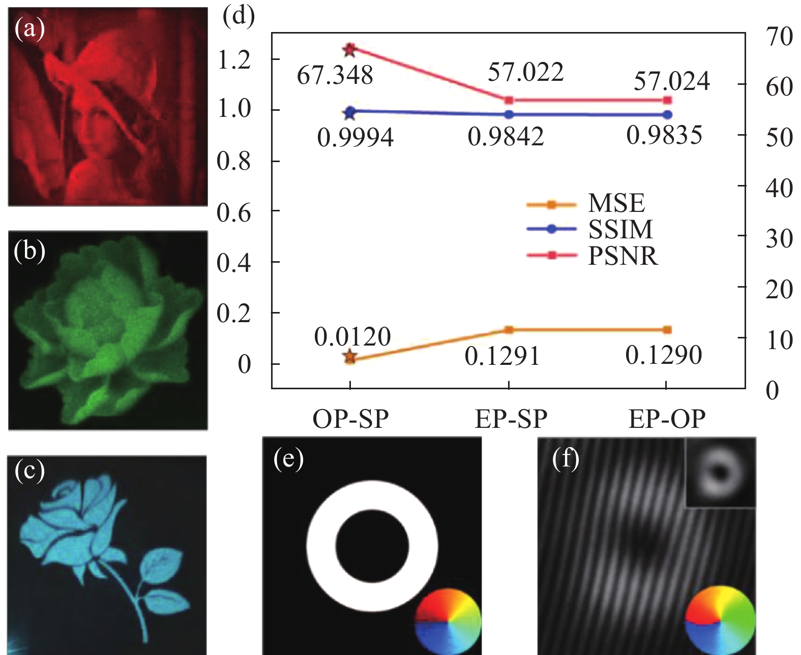
      针对上述问题,笔者提出了一种基于随机傅里叶相位编码的全息超表面设计方法,并制备了一种透射型几何相位电介质超表面,实现了在可见光波段的高质量全息显示[47],如图4(a)~(c)所示。不同于传统的编码方法,该方法利用二进制随机调制函数,将目标光场的频谱振幅编码到相位上,生成傅里叶纯相位CGH。所制备的超表面器件在633、532、488 nm波长下的工作效率分别为0.98、0.83、0.77。通过分析图像质量评价指标,包括均方误差(MSE)、峰值信噪比(PSNR)和结构相似性指数(SSIM),证明了该全息超表面在可见光波段的高质量显示性能(图4(d))。该编码技术只需一次计算即可生成CGH,避免了繁琐的迭代过程,能够有效地简化设计过程,同时具有与GS算法相似的精度。并且通过对背景噪声的分析,证明了该方法能够抑制传统全息图的散斑噪声,提供高信噪比的重建图像。

      Figure 4.  (a-c) Experimentally reconstructed holographic patterns at the wavelengths of 633 nm, 532 nm, and 488 nm, respectively; (d) Picture quality evaluation indices. OP: Original pattern, SP: numerically reconstructed pattern, EP: experimentally reconstructed pattern. The pentagrams in the graph depict the picture quality evaluation indices of the GS algorithm with 50 iterations; (e) Annual amplitude and first-order vortex phase (inset) distributions of target field; (f) Observed interferogram and demodulated amplitude (upper inset) and phase (lower inset) distributions

      此外,该编码方法并不局限于对光场的振幅重建,相位信息也可以很好地恢复,图4(e)4(f)为利用该方法重建的一阶涡旋光束。超表面在全息技术中的应用使得高质量、高分辨、高效率的全息显示成为可能,我们提出的这种全息超表面设计方法具有普适性,有利于大面积纳米全息图的制备。

    • 构造新型多自由度结构光场是光场调控领域的研究热点之一。基于振幅编码的相位调制可以实现对光场复振幅的重建[60],这为微纳尺度上复杂结构光场的构建提供了便利,在此基础上实现偏振相关的相位调控将在矢量光学、多路复用等诸多领域具有重要的应用价值。此时,单一的传输相位或几何相位已无法满足调制要求,从传输矩阵式(4)出发,当入射的圆偏振光改变为[1 −i]T时,输出场可表示为:

      与公式(5)相比较,可得:当δ=±π时,入射的左、右旋圆偏振光束在经过单元结构之后将分别转化为各自的交叉极化分量,并携带φ0+2θφ0−2θ的相位,即两正交极化分量均携带着几何相位和传输相位。因此,通过对两者的联合调控,可以给两个正交偏振分量施加独立的调制相位[17, 61]

      拓扑结构光场是近年来引起研究者们广泛关注的一类特殊结构光场,其具有与相位奇异性相关的涡旋结和链,可以作为量子力学物质波的拓扑波导[62-63]。构建光学结、链对开展拓扑量子场、拓扑流体动力场的光学模拟及关联运算等具有重要意义。拓扑结构的构建依赖于光场振幅与相位的精确再现,然而光学结、链对调制的高斯光束大小较为敏感,传统的基于空间光调制器(Spatial light modulator, SLM)的全息法实现光场重建时,存在体积大、系统复杂度高以及无法多参量调控等缺点,严重阻碍了其在微纳光学和纳米光子集成等领域的进一步研究与应用。针对这些问题并基于上述原理,笔者提出了一种能够实现多通道产生具有超小尺寸拓扑结构光场的全息电介质超表面[64]。如图5(a)所示,通过改变入射光的旋向,可以在可切换的偏振通道中实现光学涡旋结(Trefoil knot)与链(Hopf link)的产生,其横向尺度仅为220 μm,并且效率达到54.5%。

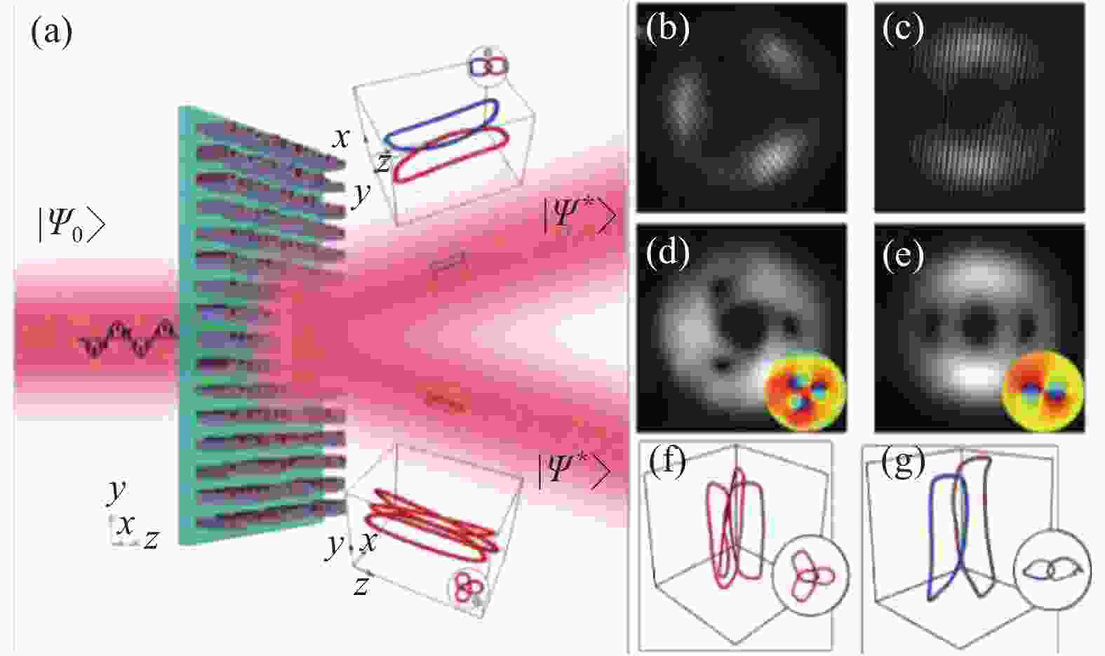
      Figure 5.  (a) Schematic of generating polarization-switchable optical vortex topologies via a holographic all-dielectric metasurface; (b) and (d), (c) and (e) Interferograms and reconstructed intensity and phase (insets) distributions of Trefoil knotted and Hopf linked fields at the z=0 plane, respectively; (f) and (g) Experimentally reconstructed configurations of Trefoil knot and Hopf link

      实现涡旋线独立拓扑结构的精确重建,是验证这种微小尺度结构光场的又一难题。笔者采用了基于数字全息术的扫描干涉测量法对拓扑结构进行了三维测量。首先记录了拓扑结构在束腰平面处的干涉图,通过数字全息物场重建得到其强度与相位分布,如图5(b)~(e)所示。随后在z方向上以500 μm为间隔扫描了多个平面并测量了其复振幅分布。为了准确地定位相位奇点并绘制拓扑结构,借助局部空间频率将相位奇点从背景中准确提取出来[65],这种方法相比于传统的过度曝光法[66-67],能够更准确地定位相位奇点位置,尤其是涡旋线在三维空间的拐点位置。最后,将多个平面的奇点分布相连,得到了相位奇点在三维空间中的分布,如图5(f)5(g)所示。同时,笔者证明了该特殊光场在微纳尺度上拓扑演化的鲁棒性,其内在的拓扑保持演化特性可能会在拓扑结构领域的光学信息处理中展现出应用潜力。

    • 随着超表面研究的不断深入,单个参量的光场调控相关研究趋于成熟,实现光场多个参量的联合调控,是超表面发展及实用化的必然趋势。完整的波前信息包含振幅与相位,因此实现振幅和相位的联合独立调控能够提高光场调控精度,尤其在实现三维全息显示中具有重要意义。

      公式(5)表明,输出场中交叉极化分量的振幅与相位分别取决于Tδφ0θ。基于此,近年来已有工作提出多种电介质超表面来实现振幅和相位的独立控制,其结构单元的Tφ0保持恒定,通过改变δθ来分别调控振幅与相位[68-69]。然而,当预期振幅不为1时,即sin(δ/2) ≠ 1,此时共极化分量振幅不再为零,这个直透分量对光场的轴向调控十分不利。针对这一情况,笔者提出并实验证明了一种可以在光轴方向上对光场进行连续调控的电介质超透镜,分别展示了具有均匀及震荡强度分布的无衍射场[70]

      首先,为了避免直接透射光的影响,需要将单元结构的相位延迟保持为δ = ±$\pi $,以消除共极化分量。此时,交叉极化分量的复振幅为Texp[i(φ0 + 2θ)],其振幅只取决于结构的传输效率,该参量由单元结构的几何尺寸决定。而相位则与传输相位和几何相位的组合有关,其中传输相位也随结构尺寸变化。为了打破这种相关性,引入一个间接参数θ'' = θφ0/2,通过在θ上增加一个相反的旋转角φ0/2来消除传输相位。此时,每个结构的输出光场具有独立可调的振幅和相位,可分别通过控制单元结构的几何参数和旋转角度进行调节,图6(a)为所选取结构的传输振幅。

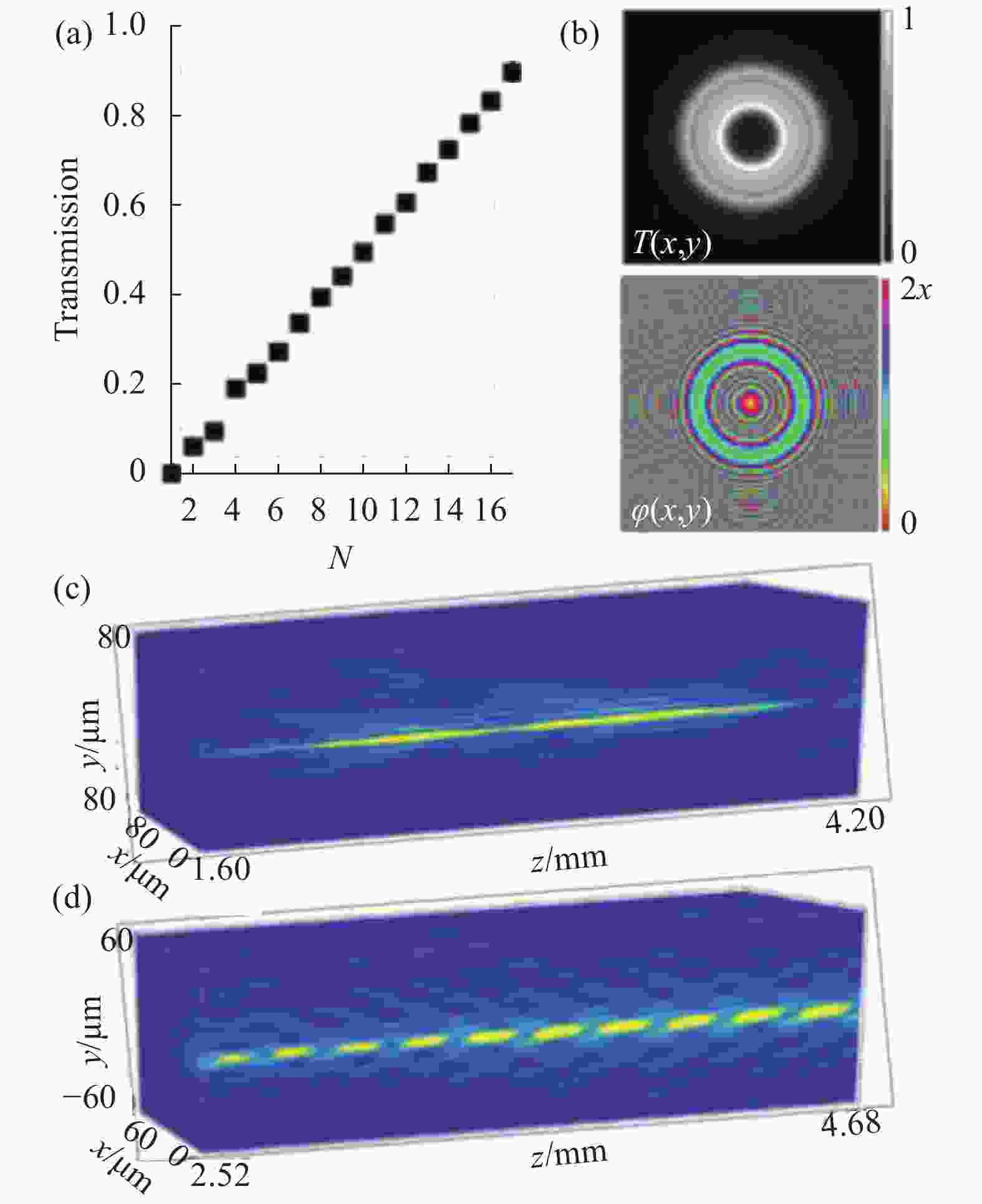
      Figure 6.  (a) Transmission amplitudes of selected geometries for the amplitude modulation; (b) Amplitude and phase distributions of the mask generated from spatial spectrum optimization; (c), (d) Experimentally measured 3D intensity distributions of two non-diffractive fields with uniform and oscillating profiles, respectively

      基于Durnin环的空间频谱优化方法,将具有任意轴向强度函数的目标光场分解成具有不同传播常数的贝塞尔分量,对其空间频谱进行优化计算即可得到最终的复振幅,如图6(b)所示。在圆偏振光入射条件下,所制备的超透镜将产生无衍射场,从而实现轴向上光场的连续调控,图6(c)6(d)为实验测量的强度在轴向上呈现均匀分布和振荡结构的光场三维结构。轴向调控为超表面光场调控添加了新的自由度,丰富了超表面的三维波前调制能力,并且可以在光学以外的其他波中实现,如声波、弹性波、物质波等。

    • 超表面突破了传统块体超材料的限制,能够在亚波长尺度上实现对光场振幅、相位、振幅灵活调控,同时具备传统光学元件无法比拟的小型化、平面化、低损耗等优点,为降低光学系统复杂度以及实现光学系统集成化提供了有效的途径,也为拓展现代光学在其他领域进一步应用奠定了基础。例如,将消色差超透镜引入光学系统代替传统的曲面透镜,可以显著减轻光学系统的负荷,促进系统集成化的发展,并在生物成像、增强现实、微机电系统等多个领域展现出巨大的应用潜力。然而正如文中所述,光场单一参量的调控局限了其进一步的应用,实现多个参量联合调控的复振幅调制,能够有效提高复杂结构光场的调制精度,同时也为超表面器件在显示、通信、测量、传感等应用中引入更多的调控自由度,是超表面发展的必然趋势。

      随着超表面研究的不断拓展与深入,研究方向已逐渐从理论基础转向应用。因此,扩展光场的可调自由度、实现器件的多功能集成、提高调控效率与工作带宽是未来超表面领域的主要研究方向。目前超表面主要通过振幅、相位、偏振这几个参量来实现对光场的调控,其多功能设计原理也大多数基于波长响应特性和偏振选择原理。因此,在光场调控中引入新的自由度能够极大地提高超表面器件的多功能集成能力,如通过频域、时域、空域等引入新的超表面调控维度;或将液晶[71]、二维材料[72]、相变材料[73]等与超表面结合,实现电控、温控等的动态调控超表面。另一方面,效率与工作带宽是影响器件性能的主要因素,多晶硅、二氧化钛等电介质材料在超表面设计中的应用极大地提高了调控效率;少层人工微结构这种新型设计方式的提出也为增强超表面结构与光场的相互作用提供了一种有效方式。

      超表面已然成为物理学及相关交叉学科研究的前沿热点。可以预见,该领域相关研究的不断进步将极大地推动现代光学向前发展,并进一步拓展其在各个领域的广泛应用。

Reference (73)

Catalog

    /

    DownLoad:  Full-Size Img  PowerPoint
    Return
    Return