


 下载:
下载:


-
光电探测器作为光学系统探测单元的核心器件常置于焦平面上,容易受激光能量作用而产生损伤效应[1]。因此,光电探测器在激光辐射下的损伤问题,一直是国际科学界的重要研究内容。
目前,国内外针对毫秒脉冲激光致探测器损伤的研究,多以单元探测器APD[2]、PIN[3]以及多元的CCD为主[4],针对硅基四象限探测器(QPD)的相关研究较少。
p-i-n型QPD为多单元位置探测器,由四个性能参数完全相同的象限构成,且各象限相对于光轴旋转对称分布,每两个象限间存在沟道,称为隔离区或死区。隔离区与I区相连接,掺杂浓度分布与I区相同,即四个P+区对应同一I区及N+区。当探测目标光束处于探测系统光轴线上时,各象限受到的光照相同,四组输出信号趋于一致;当目标成像未落在探测系统光轴上,通过各个象限不同幅值的光电流输出,可以计算获得目标成像的偏移量及偏离轴线的角度和方位,实现弱信号的精准、快速跟踪定位。但p-i-n型QPD,因具有共I区的结构,受激光辐照造成的损伤效果、损伤阈值以及损伤产生机制与PIN探测器大不不同[4]。因此,研究四个象限不均匀分布情况下的损伤效果,对QPD抗损伤、防护以及定位领域的研究有指导性意义[5-10]。
在20世纪70年代,美国海军实验室针对激光辐照下硅光电器件性能变化开展了研究[11]。Arora V. K.等[12]研究激光能量与受辐照光电探测器损伤与探测器性能下降之间的关系。美国德克萨斯大学的Steve E. Watkins等人[13],获得受10 ns的激光辐照光电探测器的反向饱和电流、击穿电压等参数,并发现其电学性能下降和表面损伤形貌现象,2013年Jostein Thorstensen等人[14-15]分析了受1.8 ms激光辐照后,硅表面损伤区域的寿命,为后续硅基探测器损伤区域寿命研究奠定基础。
针对光伏型探测器,损伤面积及形貌是激光辐照后造成QPD损伤效果、光电转换效率以及对开路电压影响的重要评价指标。选取硅基QPD进行激光辐照实验,获得了不同能量密度、不同脉宽下硅基QPD损伤面积、损伤形貌以及不同脉宽下的损伤阈值,揭示了毫秒脉冲激光对硅基QPD损伤效果的影响机制,所得研究结果为毫秒脉冲激光致探测器的损伤效果研究提供了有效实验数据支撑。
-
考虑硅基QPD结构,根据能量守恒方程以及传统热传导方程,在硅基QPD单一象限受激光辐照后温度尚未达到相变温度的实际条件下,给出不包含相变的热传导方程,如公式(1)所示:
$$\begin{split} &k\dfrac{{{\partial ^2}T(x,y,{\textit{z}},t)}}{{\partial {x^2}}} + k\dfrac{{{\partial ^2}T(x,y,{\textit{z}},t)}}{{\partial {y^2}}} + k\dfrac{{{\partial ^2}T(x,y,{\textit{z}},t)}}{{\partial {{\textit{z}}^2}}}+\\ & {Q_L} + {Q_J} = \rho C\dfrac{{\partial T(x,y,{\textit{z}},t)}}{{\partial T}} \end{split} $$ (1) 式中:
$T\left( {r,x,y,{\textit{z}},t} \right)$ ,$\rho $ ,$C$ ,$k$ 分别表示$t$ 时刻的温度场分布、材料密度、比热容、热传导率;${Q_L}$ 为激光制热热源;${Q_J}$ 为焦耳热源[2]。$${Q_L}(T,x,y,{\textit{z}},t)\! =\! {I_0}(1 \!-\! R(T))\alpha (T)f(x,y)g(t)\exp ( - \alpha (T){\textit{z}})$$ (2) 式中:
${I_0}$ 为激光光斑峰值功率;$R(T)$ 为硅的反射系数;$\alpha (T)$ 为硅的吸收系数[2];$f\left( {x,y} \right)$ 为激光光束的空间分布;$g(t)$ 为激光光束的时间分布。$${I_0} = \frac{{{I_{Avg}} \cdot \pi {r_0}^2}}{{ \displaystyle\int_0^{{r_0}} {f(x,y)2\pi \sqrt {{x^2} + {y^2}} {\rm{d}}x{\rm{d}}y} }}$$ (3) 式中:
${I_{Avg}}$ 为激光均值峰值功率;${r_0}$ 为激光光斑半径。$$f(x,y) = \exp \left( - \frac{{2\left( {{x^2} + {y^2}} \right)}}{{r_0^2}}\right)$$ (4) $$g(t) = \left\{ {\begin{array}{*{20}{l}} {1,0 < t < \tau } \\ {0,t > \tau } \end{array}} \right.$$ (5) 式中:
$\tau $ 为激光的脉宽。$$\alpha (T) = 1\;023 \times {\left( {\frac{T}{{273}}} \right)^4}[1/m],273\;{\rm K} \leqslant T \leqslant 1\;687\;{\rm K}$$ (6) $$R(T) = 0.33,273\;{\rm K} < T < 1\;687\;{\rm K}$$ (7) 初始条件为:
$${T_0} = 300\;{\rm K}$$ (8) 边界条件:
$$ - k\frac{{\partial T\left( {x,y,{\textit{z}},t} \right)}}{{\partial x}}\left| {_{x = \pm 2.45\;{\rm{mm}}}} \right. = 0$$ (9) $$ - k\frac{{\partial T\left( {x,y,{\textit{z}},t} \right)}}{{\partial y}}\left| {_{y = \pm 2.45\;{\rm{mm}}}} \right. = 0$$ (10) $$ - k\dfrac{{\partial T\left( {x,y,{\textit{z}},t} \right)}}{{\partial {\textit{z}}}}\left| {_{{\textit{z}} = 282\;{\text{μ}} {\rm{m}}}} \right. = 0$$ (11) $${Q_J} = E(T,x,y,{\textit{z}},t){J_L}(T,x,y,t)$$ (12) 式中:
$E(T,x,y,{\textit{z}},t)$ 、${J_L}(T,x,y,t)$ 为光生电流密度。基于理论研究,针对温度场进行数值计算,获得激光光斑作用上表面中心点温升变化情况,以0.5 ms计算结果为例,如图1所示。随着能量密度增加,上表面光斑作用中心点温升越快,温度峰值越高。随着能量密度超过探测器性能损伤阈值并继续增大,可造成的损伤范围越大,损伤半径和损伤深度不断増大,则掺杂离子在硅熔融阶段,向象限1内部扩散越深,范围越大,同时产生的缺陷也越来越多,象限1性能逐渐下降,并逐渐产生形貌损伤。

图 1 不同能量密度下,上表面光斑中心对应点温度随时间演化仿真关系图
Figure 1. Simulation diagram of temperature evolution with time at the corresponding point of the upper surface spot center under different energy densities
激光辐照单一象限过程中,QPD受激光辐照吸收能量,形成内部缺陷,激光强度逐渐增加,可造成探测器性能下降以及形貌损伤。因此,针对不同激光辐照QPD损伤面积、形貌展开研究。
-
在线实验装置搭建如图2所示,主要包括光学测量系统以及偏压电路系统。采用了1 064 nm Nd:YAG激光器,输出功率为0.5~10 J可调,设定脉宽范围为0.5~3.0 ms,步长设定为0.5 ms,脉冲重复频率为1~10 Hz;光学测量系统中采用了分束器对输出激光束进行分束,分束至将能量能量计和聚焦透镜;通过THORLABS DET10A/M脉宽探头和NOVAII能量计实时记录入射脉宽和能量大小。偏压电路系统中,通过 Tektronix PWS2721将偏置电压设置为40 V,还包含采样电阻、限流电阻和QPD,同时探测器其他象限的偏压电路与象限1相同。
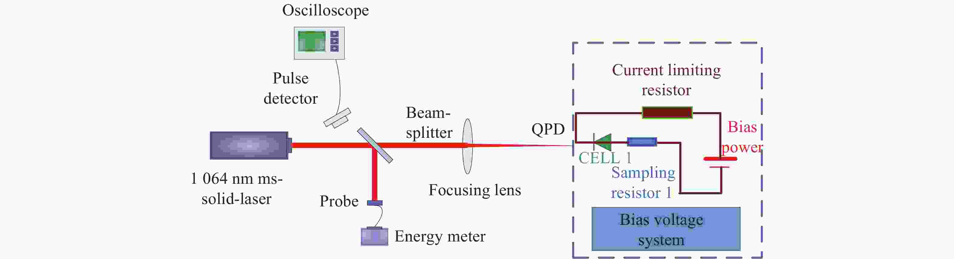
图 2 激光辐照QPD在线实验装置
Figure 2. On-line monitoring experiment configuration diagram of the QPD irradiated by laser
离线损伤形貌及面积测量系统包括DMI-5000M金相显微镜、载物片和计算机。该显微镜目镜倍率为10×,物镜倍率分别为10×、20×、50×。在毫秒脉冲激辐照QPD实验过程中,目标将产生表面剥落、褶皱、裂纹、熔坑等损伤效果。通过金相显微镜物镜和目镜两次放大,可将目标区域放大到较高倍数。为了能够清晰、完整地观察和对比分析目标损伤形貌,采用多级拍摄的方式,设置显微镜头每次以“蛇形”移动的方式自动采集2×3张图片并进行图片拼接,以获得光斑中心所在象限的完整形貌图像,利用处理软件获得损伤效果的封闭区域,并获得损伤区域面积。
所用的目标型号为GT111,其光敏表面尺寸为φ4 mm,峰值波长约为980 nm,光谱响应范围为400~ 1 100 nm,在1 060 nm左右具有较高的响应度,各个象限依次逆时针排列为象限1、2、3、4。QPD结构如图3所示。
实验是在常温、常压空气中进行的。实验过程中,使激光束聚焦在QPD的象限1时的入射激光光斑半径为285 μm,激光的空间分布为高斯分布。QPD由三维平移台控制。由于通常实际应用中QPD光敏面范围较大,且具有共I区结构,当激光作用时间较长时会对样品各象限内部结构及其粒子分布造成影响,因此,采用毫秒级脉冲激光开展此次研究。
此研究重点采用了0.5、1.0、1.5、2.0、3.0 ms(τ)毫秒脉冲激光对QPD进行辐照实验,在能量密度(I)为14.12~130.41 J/cm2的范围内,测量分析了损伤面积及损伤形貌。

图 3 GT111QPD结构剖面
Figure 3. Structure of the GT111 silicon-based QPD
-
基于如上实验条件,进行实验测量与分析,结果如下。
-
此研究对损伤后的QPD的损伤面积及损伤形貌进行了离线测量。图4所示为各脉冲作用下QPD的损伤面积随能量密度变化规律。由于QPD为多层结构,各层结构产生变化均对探测能力造成影响,因此,在判定损伤时以表面Si3N4层出现剥落时判定其表面损伤,其损伤面积记为0。随着能量密度增加,损伤面积呈上升趋势。这主要是因为,当能量密度较高时,脉冲作用时间较短,热量不能得到充分传导所造成的热应力通过局部的熔融烧蚀效应得以释放,硅基探测器所吸收的能量增加,通过晶格的弛豫过程将更多的能量传递给晶格[16],并向远离光斑中心点的四周传播,引起表面结构变化范围增大,故损伤面积增加。在不同脉宽下,损伤面积随能量密度变化整体趋势具有一致性,但在数值方面差异较大。这说明QPD损伤面积受脉宽影响。
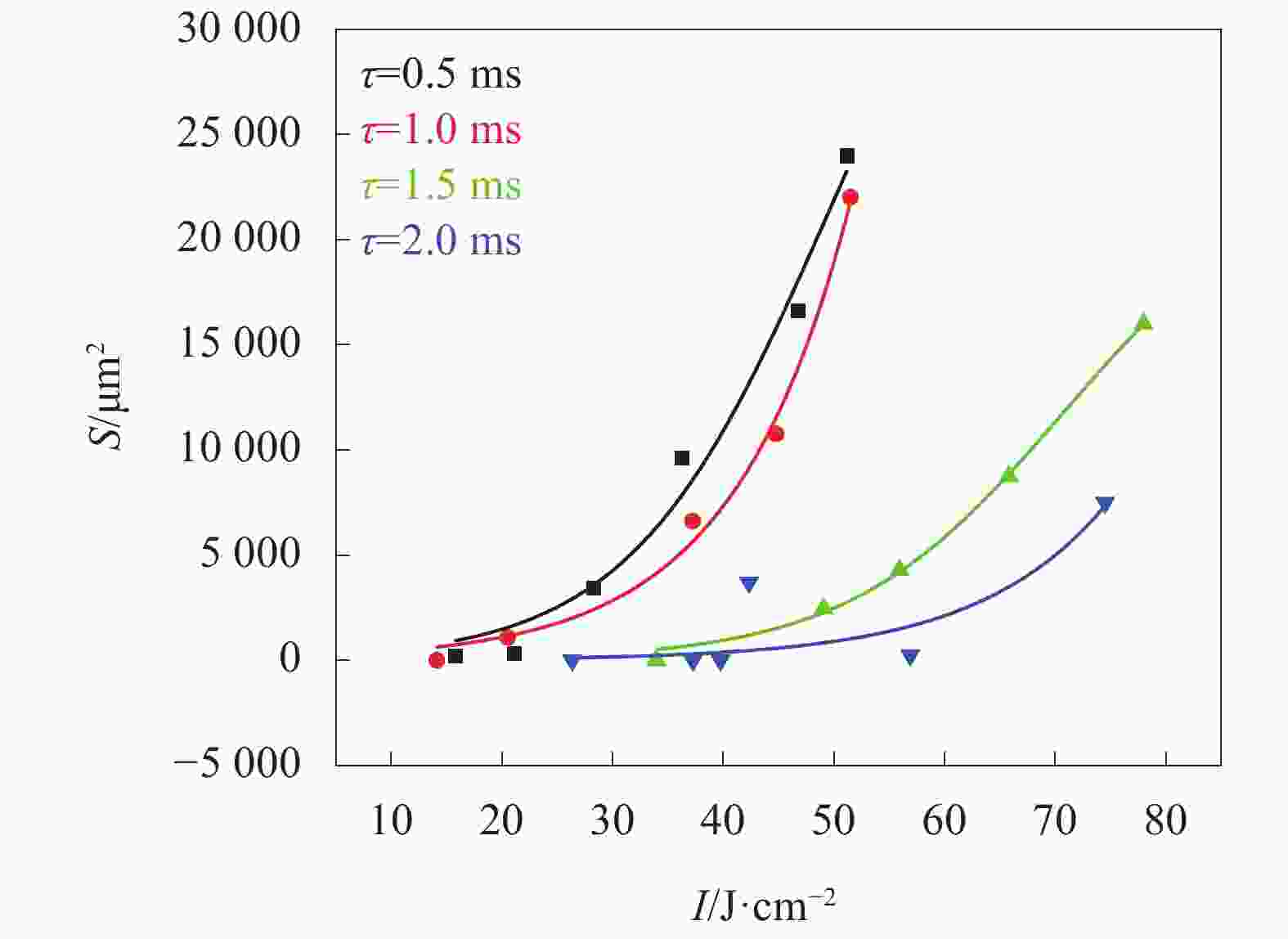
图 4 QPD损伤面积随能量密度变化关系
Figure 4. Relationship between damaged areas of QPD and energy fluence
图5为毫秒脉冲激光作用下硅基QPD的损伤面积随入射脉宽变化关系。可以看出,相同能量密度下,随着脉宽增加,损伤面积逐渐减小。这主要是因为在相同偏压、相同激光光斑作用位置、相同激光光斑面积、相同能量密度情况下,随着脉宽的增加,作用于硅基QPD上的毫秒脉冲激光在单位时间内的能量下降。这说明入射激光功率密度是毫秒脉冲激光致硅基QPD损伤面积变化的主要因素。

图 5 QPD的损伤面积随脉宽的变化关系
Figure 5. Relationship between damaged areas of QPD and pulse width
综上,在脉宽为0.5 ms情况下,当能量密度为26.39 J/cm2时,QPD损伤面积为187.00 µm2;在脉宽为1.0 ms条件下,当能量密度为20.53 J/cm2时,QPD损伤面积为1.08×103 µm2;在脉宽为1.5 ms条件下,在能量密度为49.05 J/cm2时,QPD损伤面积为2.47×103 µm2;在脉宽为2.0 ms条件下,当能量密度为26.35 J/cm2时,QPD损伤面积为126.06 µm2;在脉宽为3.0 ms条件下,当能量密度为62.76 J/cm2时,QPD损伤面积为187.00 µm2。
-
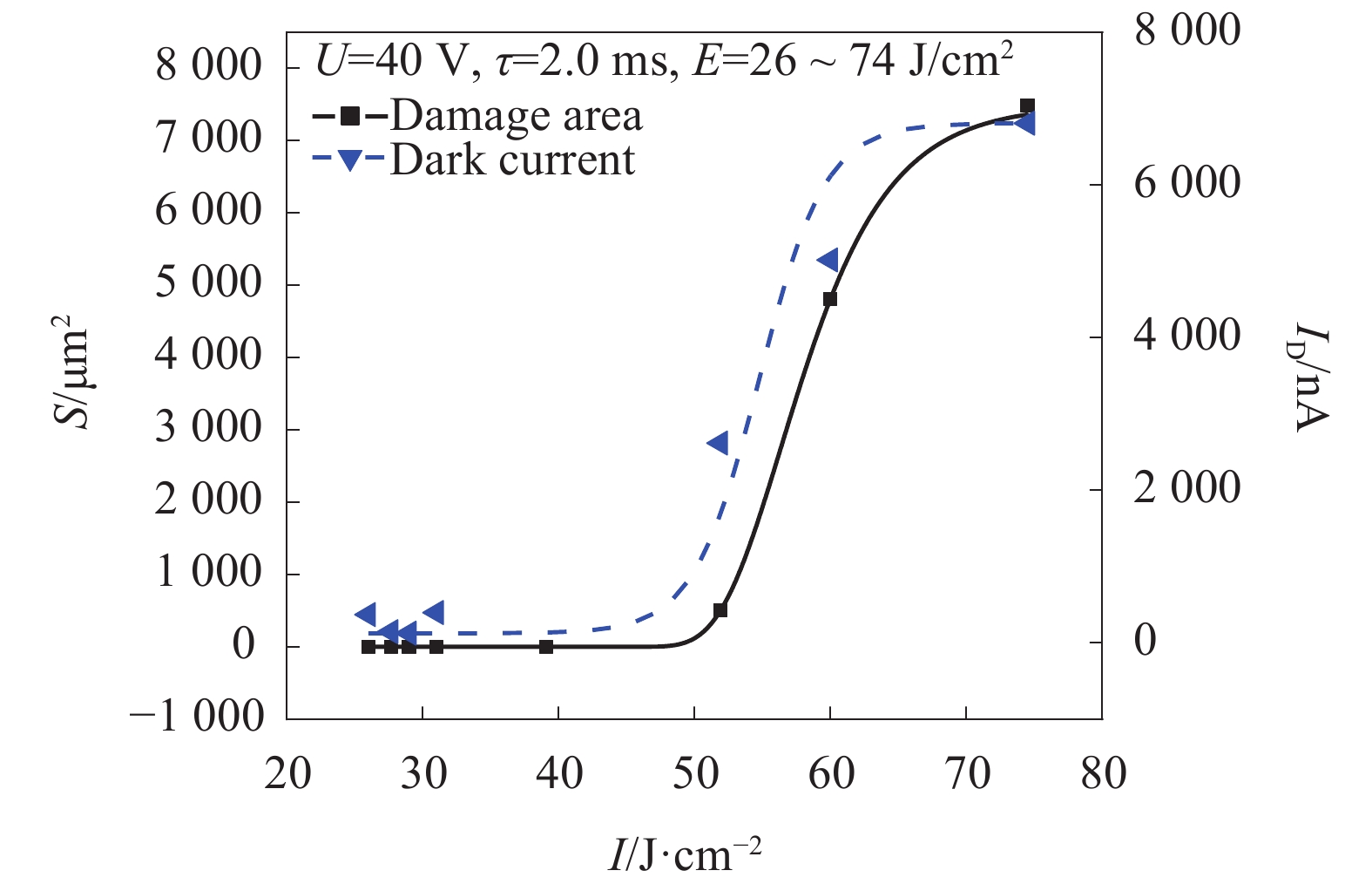
暗电流为探测器重要电学性能参数,通过离线测量系统,获得暗电流、损伤面积与能量密度的变化关系如图6所示。以2.0 ms条件实验结果为例,从图中拟合曲线可以看出,随着能量密度增加,暗电流与损伤面积变化趋势具有一定的一致性,暗电流产生量级变化的能量密度值低于产生形貌损伤的能量密度值。这足以说明,在产生形貌损伤情况下,该象限内已造成大量缺陷。
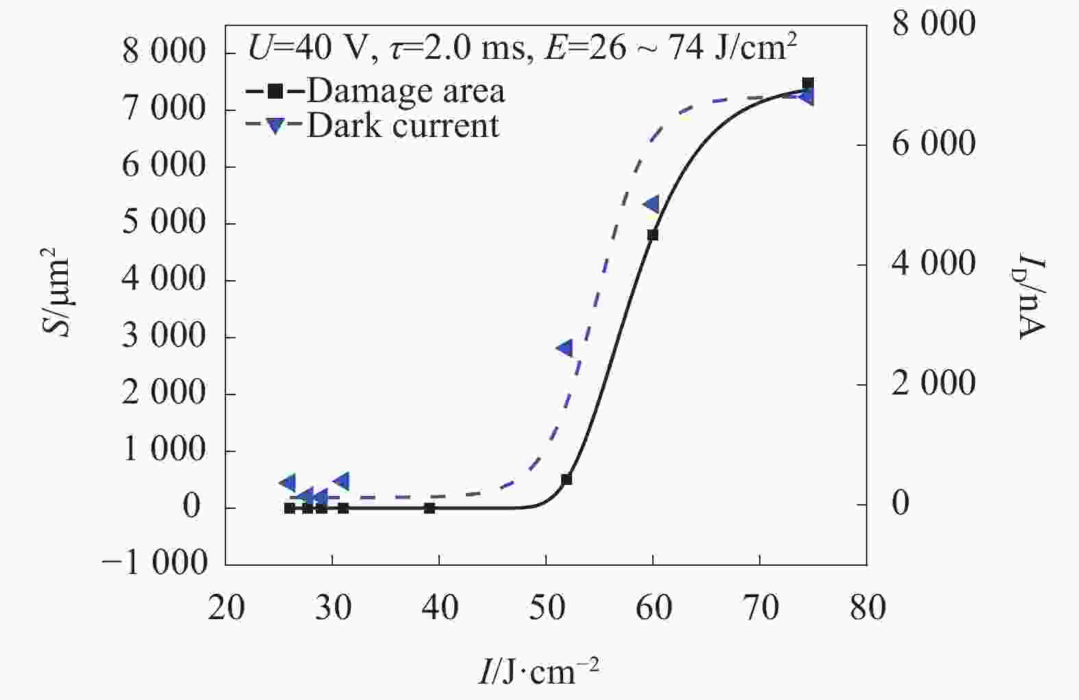
图 6 暗电流、损伤面积与能量密度三者的变化关系
Figure 6. Relationship among dark current, damage area and energy density
-
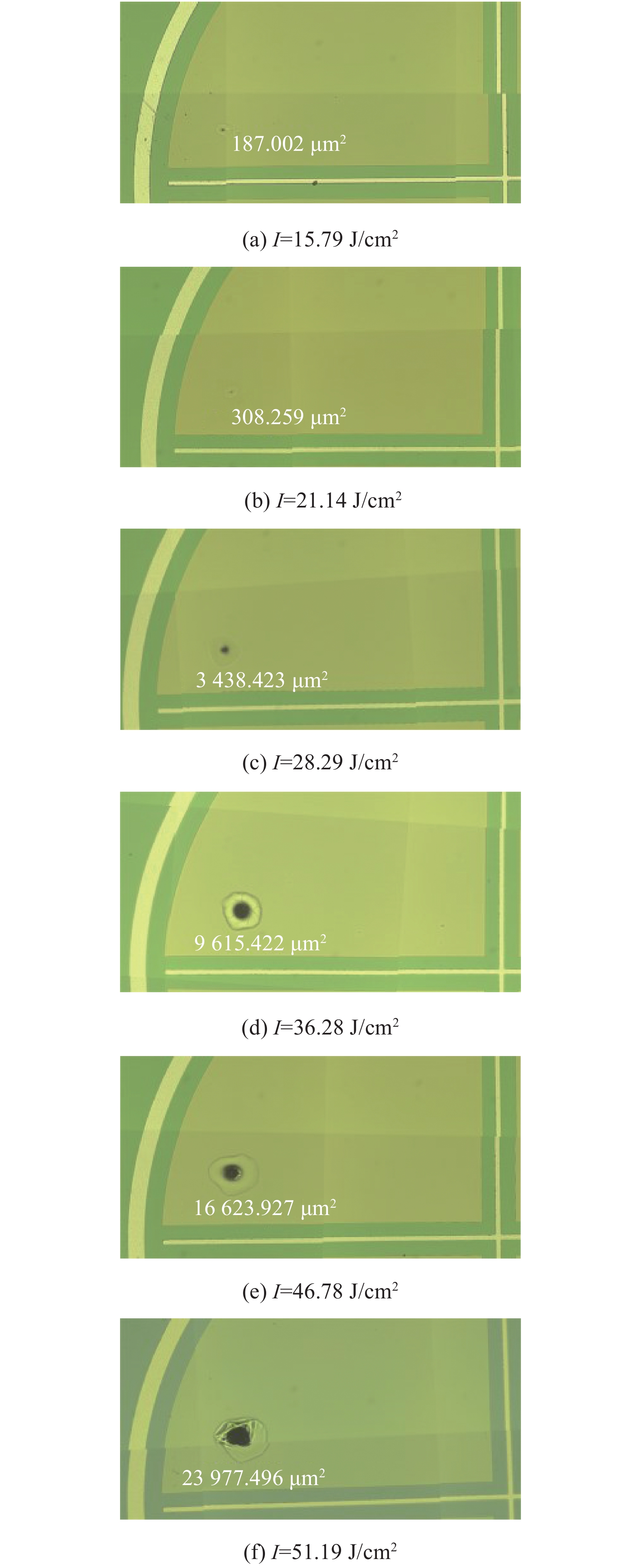
实验过程,在0.5、1.0、1.5、2.0、3.0 ms脉宽情况下,获得了不同能量密度下毫秒脉冲激光致QPD损伤形貌,以0.5 ms下损伤形貌为例,如图7所示。激光辐照QPD致使探测器产生了表面剥落、褶皱、裂纹、熔坑等现象。产生不同损伤效果的原因如下:随着探测器内部温度升高,硅材料的吸收系数逐渐增加,而热传导率逐渐降低,促使QPD激光光斑所在象限内部产生较大的温度梯度,同时,高温会使材料由脆性变为塑性,屈服强度会大大降低。当最大热应力超过临界应力时,硅材料将产生塑性变形和脆性裂纹,这些沿解理面发生的塑性变形[4]。

图 7 τ=0.5 ms,I=15.79~51.19 J/cm2,QPD损伤形貌图像
Figure 7. τ=0.5 ms,I=15.79-51.19 J/cm2,damaged morphology on the upper surface of QPD
τ=0.5 ms,I=15.79 J/cm2时QPD出现熔融损伤,在脉宽为1.0、1.5、2.0、3.0 ms QPD表面剥落图如图8所示,产生表面剥落的能量密度值约为14.12 J/cm2、33.94 J/cm2、39.76 J/cm2和47.62 J/cm2。产生表面剥落的能量密度值逐渐增加的原因是,QPD损伤形貌主要受功率密度影响。具体分析如下:1) 相同光斑面积下,单位时间内,脉宽增加,作用在QPD单一象限上的能量降低,因此,产生剥落所需能量密度越高;2) 由于毫秒脉冲激光作用时间较长,使得热量有足够的时间传导致靶材内部,且QPD共I区以及基底层,载流子不仅将能量传递至光斑所在象限内部晶格,还传递至其他象限内部晶格,能量在光斑所在象限内的累积减弱,因此,产生剥落所需能量密度增加,但该过程将促使其他象限产生内部缺陷[16-17]。
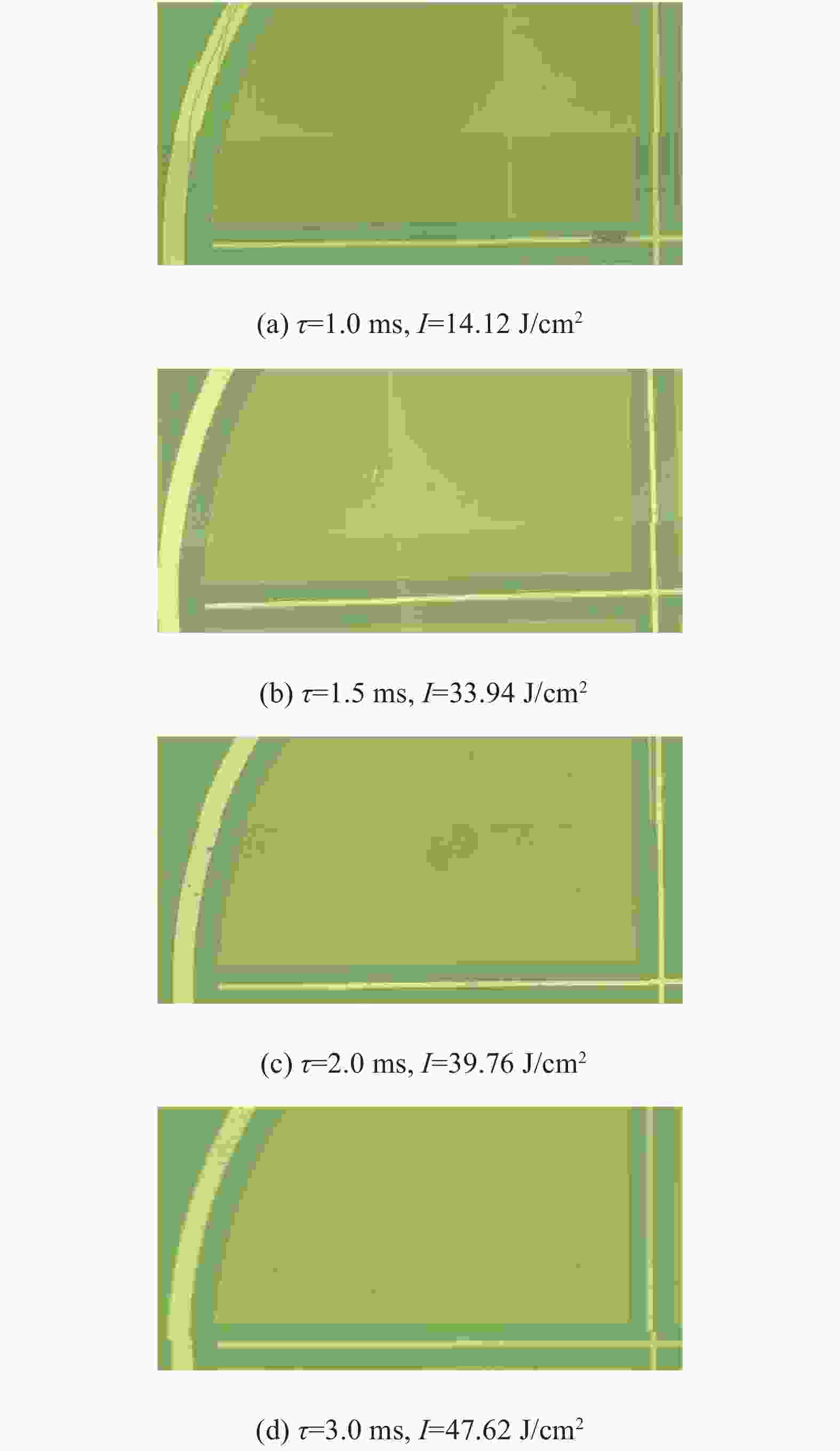
图 8 不同脉宽下,脉冲激光辐照后QPD表面剥落图像
Figure 8. Surface peeling on the upper surface after pulse laser irradiation under different pulse widths
-
基于二维显微测量技术,测量分析了毫秒级激光辐照下p-i-n QPD的损伤形貌。在脉宽为0.5~3.0 ms时,通过分析不同能量密度下的QPD单一象限的损伤面积、损伤形貌,论证得到:在毫秒级脉冲激光作用下,QPD损伤面积随能量密度增加逐渐增加,且随脉宽增加逐渐降低;随能量密度增加,QPD产生表面剥落、褶皱、裂纹、熔坑等损伤效果,且当能量密度增加到一定阈值时,损伤面积增速开始缓慢。并且进行测量。实验结果表明,在脉宽为0.5 ms,能量密度为15.79 J/cm2情况下,QPD出现熔融损伤,当脉宽为1.0、1.5、2.0、3.0 ms, QPD出现表面剥落的能量密度值为14.12、33.94、39.76、47.62 J/cm2。
综上,通过严谨的实验测量及论证分析,为毫秒级脉冲激光致QPD及多元探测器的损伤效果研究提供了实验数据支撑,对QPD抗损伤、防护以及跟踪定位领域的相关研究有指导性意义。
Experimental study on damage area and morphology of silica-based QPD induced by long pulse
-
摘要: 为了研究硅基QPD在不同能量密度、不同脉宽激光辐照下的损伤面积、形貌,基于二维显微测量技术,测量了硅基QPD单一象限的损伤面积、形貌随激光能量密度和脉宽的变化。结果表明,在毫秒脉冲激光作用下,硅基QPD产生表面剥落、褶皱、裂纹、熔坑等损伤效果,且主要受入射激光功率密度影响,损伤面积随激光能量密度逐渐增加,随脉宽增加逐渐降低。通过实测分析,得出了不同激光脉宽下,硅基QPD表面形貌损伤阈值。激光脉宽为0.5 ms,能量密度为15.79 J/cm2时,硅基QPD出现熔融损伤;而脉宽为1.0、1.5、2.0、3.0 ms时,硅基QPD出现表面剥落的能量密度值为14.12、33.94、39.76、47.62 J/cm2。Abstract: Based on two-dimensional metallographic microscopic measurement technology, the damage area and morphology of the silicon-based quadrant photo-detector(QPD) were studied under different laser energy fluences and pulse widths. The damage area and morphology of silicon-based QPD with single cell change with laser energy fluences and pulse width were measured. The results showed that, the QPD produced surface pooling, folding, cracks, ablation areas and other damage effects under the action of a millisecond pulse laser. The damage area mainly affected by the incident laser energy fluences, and the damage area gradually increased with the laser energy fluences and decreased with the increase of pulse width. The damage thresholds of a silicon-based QPD with different laser pulse widths were obtained. At 0.5 ms, and the energy fluences was 15.79 J/cm2, the silicon-based QPD produced melting damage, and the energy fluences values of surface-damaged thresholds in the silicon-based QPD with pulse widths of 1.0, 1.5, 2.0 and 3.0 ms are 14.12 J/cm2, 33.94 J/cm2, 39.76 J/cm2 and 47.62 J/cm2.
-
Key words:
- long pulse /
- silicon-based quadrant photo-detector /
- damage morphology /
- damage threshold
-
图 1 不同能量密度下,上表面光斑中心对应点温度随时间演化仿真关系图
Figure 1. Simulation diagram of temperature evolution with time at the corresponding point of the upper surface spot center under different energy densities
图 2 激光辐照QPD在线实验装置
Figure 2. On-line monitoring experiment configuration diagram of the QPD irradiated by laser
图 4 QPD损伤面积随能量密度变化关系
Figure 4. Relationship between damaged areas of QPD and energy fluence
图 5 QPD的损伤面积随脉宽的变化关系
Figure 5. Relationship between damaged areas of QPD and pulse width
图 6 暗电流、损伤面积与能量密度三者的变化关系
Figure 6. Relationship among dark current, damage area and energy density
图 7 τ=0.5 ms,I=15.79~51.19 J/cm2,QPD损伤形貌图像
Figure 7. τ=0.5 ms,I=15.79-51.19 J/cm2,damaged morphology on the upper surface of QPD
-
[1] Kruer M, Esterowitz L, Allen R, et al. Thermal models for laser damage in InSb photovoltaic and photoconductive detectors [J]. Infrared Physics, 1976, 16(3): 375-384. doi: 10.1016/0020-0891(76)90064-6 [2] Wang D, Wei Z, Jin G Y. Experimental and theoretical investigation of millisecond-pulse laser ablation biased Si avalanche photodiodes [J]. International Journal of Heat and Mass Transfer, 2018, 122: 391-394. doi: 10.1016/j.ijheatmasstransfer.2018.01.096 [3] Wei Z, Zhang W, Wang D. Structural, optical and electrical behavior of millisecond pulse laser damaged silicon-based positive-intrinsic-negative photodiode [J]. Optik, 2017, 131: 110-115. doi: 10.1016/j.ijleo.2016.11.074 [4] Zhang Zhen, Zhou Menglian, Zhang Jianming. Shadows of laser spots in CCD and their mechanism [J]. Optics and Precision Engineering, 2013, 21(5): 1365-1371. (in Chinese) doi: 10.3788/OPE.20132105.1365 [5] Zhao Xin, Tong Shoufeng, Jiang Huilin. Experimental testing on characteristics of four-quadrant detector [J]. Optics and Precision Engineering, 2010, 18(10): 2165-2170. (in Chinese) doi: 10.3788/OPE.20101810.2164 [6] Lin Zhiqi, Li Huijie, Lang Yonghui. A study on obtaining the facula parameters of quadrant photodetectors through fretting [J]. Optics and Precision Engineering, 2009, 17(4): 764-770. (in Chinese) [7] Guo Ming, Zhang Yongxiang, Zhang Wenying, et al. Thermal damage of monocrystalline silicon irradiated by long pulse laser [J]. Infrared and Laser Engineering, 2020, 49(3): 0305002. doi: 0305002 [8] Zhang M, Nie J, Sun K, et al. Numerical analysis on thermal function of single crystal silicon irradiated by combined laser [J]. Infrared and Laser Engineering, 2018, 47(11): 1106011. (in Chinese) doi: 10.3788/IRLA201847.1106011 [9] Zheng Changbin, Shao Junfeng, Li Xuelei, et al. Femtosecond pulsed laser induced damage characteristics on Si-based multi-layer film [J]. Chinese Optics, 2019, 12(2): 371-381. (in Chinese) doi: 10.3788/co.20191202.0371 [10] Yang H D, Li X H, Li G Q, et al. Surface morphology of silicon induced by 532 nm nanosecond laser under different ambient atmospheres [J]. Chinese Optics, 2011, 4(1): 86-92. (in Chinese) [11] Kruer M, Allen R, Esterowitz L, et al. Laser damage in silicon photodiodes [J]. Optical and Quantum Electronics, 1976, 8(5): 453-458. doi: 10.1007/BF00624835 [12] Arora V K, Dawar A L. Laser-induced damage studies in silicon and silicon-based photodetectors [J]. Applied Optics, 1996, 35(36): 7061-7065. doi: 10.1364/AO.35.007061 [13] Watkins S E, Zhang C Z, Walser R M, et al. Electrical performance of laser damaged silicon photodiodes [J]. Appl Opt, 1990, 29(6): 827-835. doi: 10.1364/AO.29.000827 [14] Thorstensen J, Foss S E. Investigation of depth of laser damage to silicon as function of wavelength and pulse duration [J]. Energy Procedia, 2013, 38: 794-800. doi: 10.1016/j.egypro.2013.07.348 [15] Thorstensen J, Foss S E. New approach for the ablation of dielectrics from silicon using long wavelength lasers [J]. Energy Procedia, 2013, 38: 787-793. [16] Sze S M, Kwok K Ng. Physics of Semiconductor Devices[M]. 3rd ed. Translated by Gen Li, Zhang Ruizhi. Xi'an: Xi'an Jiaotong University Press, 2008. (in Chinese) [17] Marquardt C L, Giuliani J F, Fraser F W. Observation of impurity migration in laser-damaged junction devices [J]. Radiation Effects, 1974, 23(2): 135-139. doi: 10.1080/00337577408232055 -

 点击查看大图

计量
- 文章访问数: 362
- HTML全文浏览量: 98
- PDF下载量: 25
- 被引次数: 0


