


 下载:
下载:


-
In the last decade, InGaAs detectors for the near infrared wavelength range from 1.0 to 1.7 μm have made crucial progress with the development of high-speed receivers for fiber optic telecommunications [1-2]. InGaAs/InP Avalanche Photo Diodes (APDs) for fiber optic telecommunications are reversed bias pn junctions operated in "Linear-mode" [3]. The output photocurrent is proportional to input optical power in this mode. Excellent characteristic performance APDs benefit from internal gain owing to impact ionization is developed for high gain-bandwidth and low excess noise application. However, single photon detectors supply a macroscopic electrical pulse in response to a single photon irradiating on the APD. Single Photon Avalanche Diodes (SPADs) are pn junctions which are biased over breakdown voltage (Vbr) which operate in the so-called "Geiger-mode" [4]. A single photon irradiating can trigger a self-sustaining electron hole generation event that leads to a macroscopic current pulse. Devices working in this mode can provide the capability to accurately detect the arrival at the SPAD of a single photon[5].
In previous reports, Mark A. Itzler et al. of Princeton Lightwave Inc basically achieved a dark count rate (DCR) of 3.21 kHz with a 20.3% photon detection efficiency (PDE) in the 128 × 32 array SPADs, and the uniformity was excellent in 2018[6]. X. Meng et al. achieved the above parameter index on a single SPAD in 2014 [7].They also achieved 26% PDE based on InGaAs/InAlAs with DCR of 1×10⁵ kHz in 2016[8]. J. Wen group discussed and analyzed the source mechanism of dark current in 2018[9]. This group achieved 70% PDE with the DCR of 48 kHz at 226 K working in gated-mode and the after pulse probability (APP) remained below 2.2% for PDE up to 62.7% in 2020[10]. By performing structure design optimization with a dielectric-metal reflection layer, Y. Fang et al. reached 60% PDE with DCR of 340 kHz in 2020 [11]. Generally speaking, the SPAD's challenges are mainly in two aspects. On the one hand, how to tradeoff PDE, DCR, APP and other parameters according to different application scenarios [12]. On the other hand, the latest development of InGaAsP SPAD emphasizes the trend of integrating SPADs into large-format arrays. Pixel miniaturization, high resolution and non-uniformity bias voltage correction are imperative parameters for array applications[13].
SPADs are indispensably cooled to suppress the dark counts for photon-counting applications. The working temperature is crucial to the SPAD performance. In this paper, The InGaAs/InP SPAD working at a wavelength of 1 550 nm is designed and characterized. We describe SPAD design concepts, specific fabrication process and the resulting internal structure. The temperature influence on SPAD is investigated, including the origin of the dark count rate (DCR), the photon detection efficiency (PDE) and the after pulse probability performance (APP). The above temperature influence analysis, discussion and calculation can provide more theoretical basis and support for the design and fabrication of SPAD.
-
The left of Figure 1 shows cross-section of the SPAD structure. The diameter of the SPAD is 25 μm. We use the metal organic chemical vapor deposition (MOCVD) method to grow separate absorption, gradation, charge and multiplication epitaxial layers (SAGCM) on a (100) S-doped InP substrate. This type of SPAD use wide band gap InP as the multiplication layer, and narrow band gap InGaAs as the absorption layer. There is a charge layer between the absorption and the multiplication layer. Its function is to control the internal electric field distribution of the device, so that the multiplication layer has enough electric field strength to cause avalanche multiplication while avoiding the high electric field intensity of the absorption layer and causing large tunneling dark currents. The electric field distribution is shown in the right of Figure 1. To begin with, a typical layer structure consists of a 1 μm InP buffer layer and a doping density of 1 × 1017 cm−3, followed by a 2 μm thick undoped Ga0.467In0.533As light absorption layer with a background doping concentration of less than 1 × 1015 cm−3. Moreover, three undoped InGaAsP graded layers are grown to prevent holes from accumulating at the hetero interface between InP and InGaAs. At last, a Si-doped 130 nm InP charge layer with a doping density of 2×1017 cm−3 and a 3.5 μm undoped InP cap layer are grown[14].
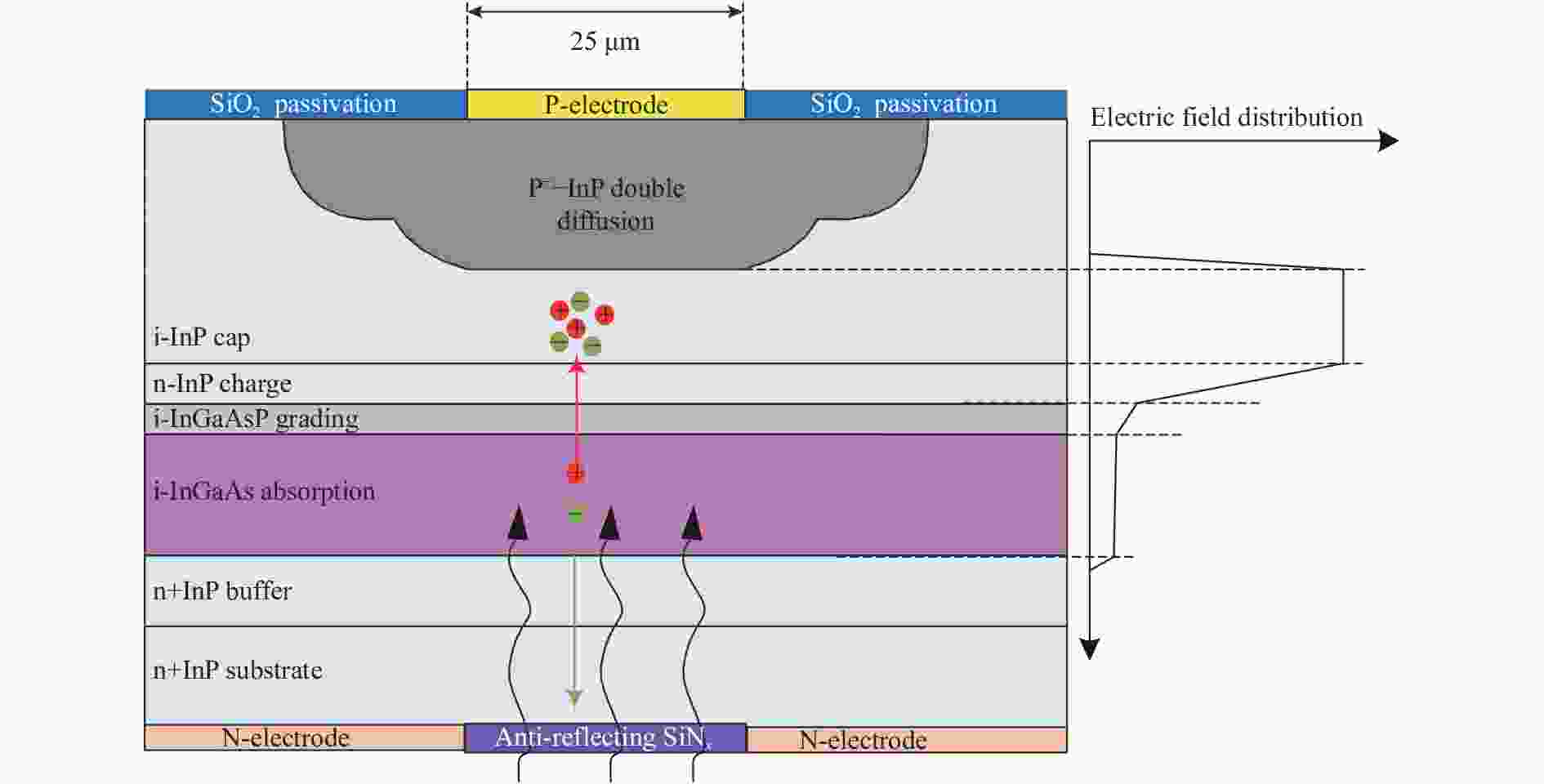
Figure 1. Cross-section of the SPAD structure and its internal electric field distribution
The cross configuration of the SPAD is defined by employing the diffusion of Zn doping atoms through the diffusion window patterned by the SiO2 dielectric passivation layer to create a buried p-n junction. The two-dimensional electric field distribution produced by single diffusion tends to show electric field peaks and related edge breakdown effects near the edge of the quasi-cylindrical junction. In order to clamp down edge breakdown, two concentric diffusions method is used to make the p-n junction deeper in the center area of the diode than in the outer area. Compared with the center of the device, the wider multiplication area at the periphery of the device has lower peak electric field strength and a higher breakdown voltage[15]. Therefore, avalanche breakdown is limited to the central area of the structure. This buried junction plane geometry supply low perimeter leakage and steady long-life operation, and the diode platform shows outstanding reliability. P-metallization is achieved by photolithographic lift off Ti/Au contact. Then the substrate is thinned and polished in order to reduce resistance and facilitate dissociation and packaging. The incident aperture is coated with anti-reflecting SiNx
, to eliminate the reflection from the air-InP interface. The outside region of the aperture is capped with AuGeNi/Au for N-electrode contact by photolithographic lift off. Finally, the SPAD fabrication is finished by annealed the electrode at 400 ℃ for 1 minute. -
Plot of the dark current (Id) and photocurrent (Ip) at 1550 nm as a function of bias voltage for a typical SPAD are obtained by current-voltage (I-V) measurement at temperature of 223-293 K and shown in Figure 2(a). It can be seen from Ip that the punch-through voltage (Vpt) is 35 V. This is desirable because such a high Vpt provides low electric field in the absorption region results in a small tunneling current. The responsivity of the SPAD is 0.9 A/W at Vpt, providing an external quantum efficiency of 72%. The operating voltage when Id is 10 μA is defined as the breakdown voltage (Vbr). The Id at 95% Vbr is 1 pA and 392 pA at 223 and 293 K, respectively. Such low Id indicates that the epi-wafer of the SPAD has excellent crystalline quality. The temperature dependency of the Vbr is shown in the Figure 2(b). The Vbr increases with increasing temperature. This is because the ionization coefficient decreases at elevated temperatures, and the threshold of electric field strength in multiplication region required for breakdown increases, which in turn causes the increase of the Vbr.

Figure 2. (a) Dark current and photocurrent at 1 550 nm as a function of bias voltage for SPAD at temperature of 223-293 K;(b) Breakdown voltage versus temperature data (symbols) and linear fitting (line)
The temperature dependency coefficient, ΔVbr/ΔT, is listed to be 100 mV/K from 53.3 V at 223 K to 60 V at 293 K. The SPDE ΔVbr/ΔT can be calculated using the following expression[16]:
$$ \frac{{\Delta {V_{{\rm{br}}}}}}{{\Delta T}} = \left[ {\left( {42.5 \times {X_{\rm{d}}}} \right) + 0.5} \right] \times \frac{\omega }{{{X_{\rm{d}}}}} $$ (1) where Xd and ω are the thickness of the multiplication layer and the total width of the depletion region respectively. It can be seen that the ΔVbr/ΔT is negatively correlated with the thickness of the multiplication layer and positively correlated with the width of the depletion region. The improvement of temperature characteristics requires the cooperation between the two factors.
As we know that SPADs are pn junctions that are biased above Vbr and operate in the so-called " Geiger mode "[17]. The SPAD is operated in gated mode in order to avoid damage to the SPAD due to long-term macroscopic current pulse[18]. The gate duration of the biased electrical pulses is 2.2 ns with a repetition frequency (f) of 1 MHz. The PDE of SPAD can be expressed as:
$$ PDE = {P_{{\rm{trigger}}}} \times QE $$ (2) where Ptrigger and QE are the probability of avalanche triggering and the absorption efficiency, respectively. The former is mainly determined by the thickness of the multiplication InP layer and the electric field in it. The latter depends on the thickness of depletion region in the absorption InGaAs layer that is determined by the epitaxial growth of the SPAD [7, 19]. Figure 3 shows PDE and DCR with temperature when the SPAD operating at Geiger-mode under an excess bias of 2 V higher than Vbr. For the typical sample device, the PDE increase from 13.69% to 20.7% and the DCR decreases from 500 kHz to 4.09 kHz over the temperature range from 293 to 223 K. PDE increases toward lower temperatures. This is because: (1) At a constant excess bias, due to the decrease in breakdown voltage, the electric field from OFF to ON in the multiplication area at lower temperatures increases more strongly, so the PDE is higher; (2) The probability of avalanche triggering (Ptrigger) enhances due to the higher impact ionization coefficient at lower temperatures.

Figure 3. Temperature dependence of PDE and DCR of 25 μm diameter SPADs (color online)
Activation energies are calculated from the trend of DCR with temperature to investigate the source of the dark current and DCR[8]. DCR and dark current are closely related. The major source of dark current is related to generation-recombination current, surface leakage current, and tunneling current. The generation-recombination current passes through the multiplication region and has a great impact on DCR. The surface dark current does not participate in the multiplication process and does not contribute to the DCR. The tunneling current is also very weak at this operating temperature range (223-293 K) and will not contribute to the extra DCR. From this we can infer that the dark count is basically generated by the thermal generation. The DCR origin from thermal generation can be expressed as:
$$ {\rm{DCR}} \propto {n_{\rm{i}}}/{\tau _{\rm{e}}} \propto {T^2}\mathit{{\rm{exp}}}\left( { - {E_{\rm{a}}}/kT} \right) $$ (3) where ni and τe are the intrinsic carrier density and the effective lifetime, respectively, Ea is the activation energy, k is Boltzmann constant, and T is the temperature. The value of Ea can be obtained by linear fitting ln (DCR/T2) versus 1/kT. As shown in Figure 4, the fitted Ea is 0.35 eV for the DCR from 223 to 293 K. This activation energy is close to half of the band gap (0.375 eV) of the Ga0.467In0.533As (Eg=0.75 eV) absorption layer, indicating that the thermal generation in the absorption layer is dominant for the DCR in this temperature range. The method of using DCR with temperature to calculate the activation energy to obtain the source of the dark current and DCR is also involved in the references of related articles [8-9, 20]. However, the conclusions obtained are different according to the operating temperature of the SPAD.

Figure 4. Activation energies of DCR at 2 V excess bias
Figure 5 shows the PDE and DCR dependence on excess bias of 25 μm diameter SPAD at 223 K. The PDE can be increased by operating at a higher excess bias voltage Vex, where Vex = V – Vbr is the bias in excess of Vbr. However, the DCR also increases with higher Vex. For a SPAD with excellent characteristics, it is generally hoped that its PDE is high enough while maintaining a low DCR, which requires tradeoff between PDE and DCR. The SPAD made in this article shows excellent detection characteristics, the PDE is 25.72% at 1 550 nm wavelength and the DCR is 9.09 kHz at 3 V excess bias.

Figure 5. PDE and DCR dependence on excess bias of 25 μm-diameter SPAD at 223 K
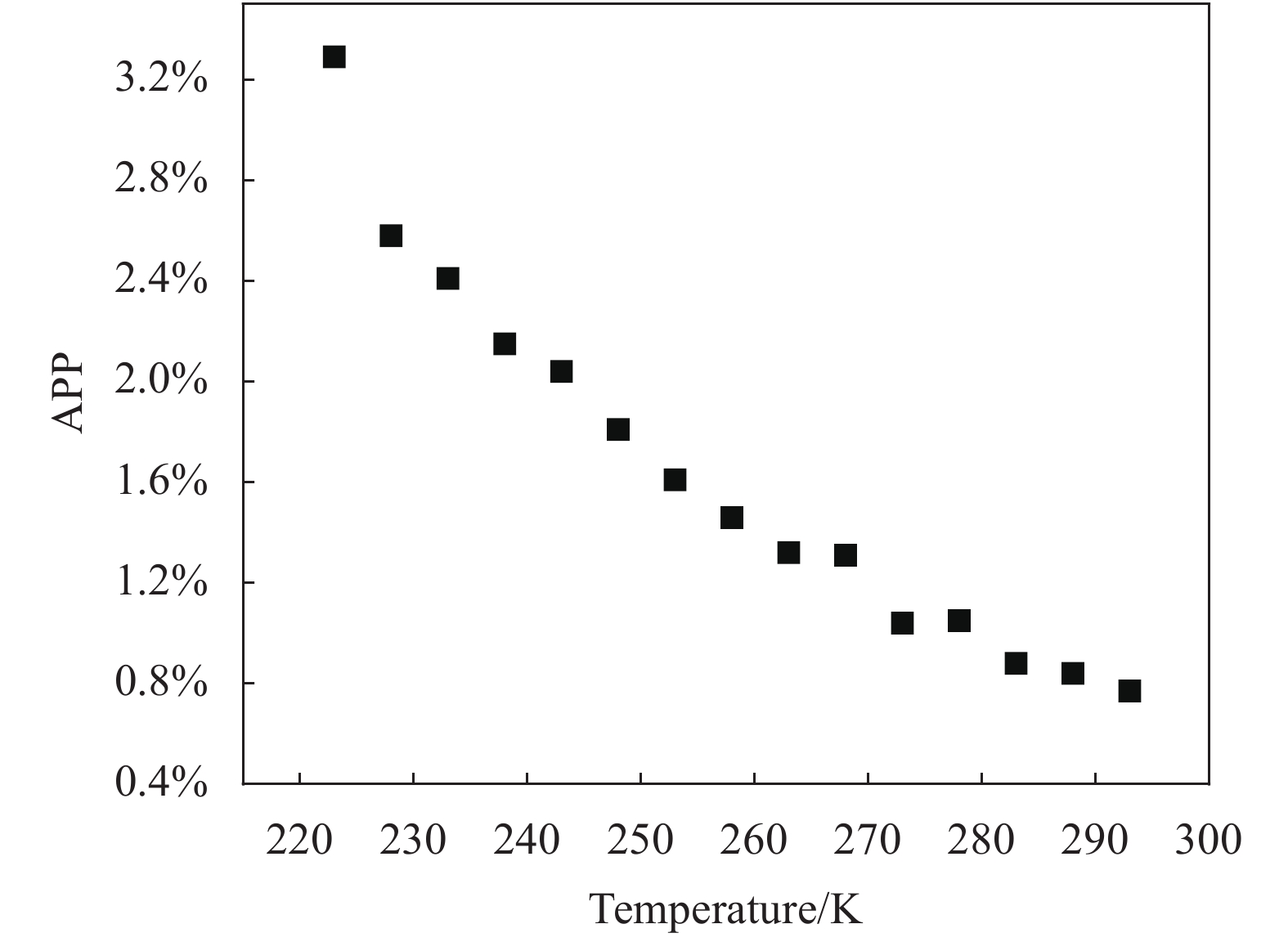
There are inevitable defects in the material of SPAD. These defects will trap carriers in the avalanche process[21]. These carriers will be slowly released. Trapped carriers may also cause an avalanche event, resulting in APP counting before the release completed[22]. In the case of high repetition frequency and low temperature, the APP is the main factor related to the DCR. As shown in Figure 6, we test the relationship between the APP and the temperature. It can be seen from the figure that the APP gradually decreases from 3.29% to 0.77% at the operating temperature range 223-293 K. This is because the operating temperature increases and the carriers trapped by the defects can be released more quickly. So considering the APP, there is an optimum operating temperature.

Figure 6. Relationship between APP and the operate temperature at 2 V excess bias
-
In summary, we have demonstrated InGaAs/InP SPAD to detect 1 550 nm wavelength photons. Its breakdown voltage dependency with temperature is approximately 100 mV/K. Using Geiger-mode operation, the SPAD exhibit a photon detection efficiency of 21% at 1 550 nm with a dark count rate of 4.1 kHz and a after pulse probability of 3.29%. These performances make the presented InGaAs/InP SPAD excellent candidates for advanced 3D imaging laser radar system and quantum communication at 1550 nm. We have also presented a physical mechanism discussion of temperature dependence on PDE and DCR for a typical SPAD. The analysis results show that the PDE increases as the temperature decreases is mainly due to the lower the temperature, the higher the probability of avalanche triggering and the increase of the electric field in the multiplication area. The main source mechanism of DCR is analyzed through the calculation of activation energy. The calculation results indicate that the thermal generation in the absorption layer is dominant for the DCR. The mechanism of APP affecting the dark count rate is discussed, and it is concluded that the temperature of the SPAD working at Geiger-mode is not as low as possible. The above mechanism analysis, discussion and calculation can provide more theoretical basis and support for the design and fabrication of SPAD.
Temperature dependency of InGaAs/InP single photon avalanche diode for 1 550 nm photons
-
摘要: 在越来越多的光子计数应用中,用于近红外光波长领域的单光子探测器受到广泛关注。例如在量子信息处理、量子通信、3D激光测距(LiDAR)、时间分辨光谱等光子计数应用领域。文中设计并展示了用于探测1 550 nm波长光子的InGaAs/InP单光子雪崩二极管(SPAD)。这种SPAD 采用分离吸收、过渡、电荷和倍增区域结构 (SAGCM),在盖革模下工作时具有单光子灵敏度。SPAD的特性包括随温度范围223~293 K变化的击穿电压、暗计数率、单光子检测效率和后脉冲概率。25 μm 直径的 SPAD 显示出一定的温度相关性,击穿电压随温度的变化率约为100 mV/K。当SPAD在盖革模式下温度为223 K工作时,在暗计数率为4.1 kHz,后脉冲概率为3.29%的基础上,对1 550 nm光子实现了21%的单光子探测效率。文中还分析和讨论了SPAD温度相关性的单光子探测效率、暗计数率和后脉冲概率的来源和物理机制。这些机制分析、讨论和计算可以为SPAD的设计和制备提供更多的理论支持和依据。Abstract: Single-photon detectors for the near-infrared wavelength region are receiving widespread attention in an increasing number of photon counting applications. In fields such as quantum information processing, quantum communication, 3-D laser ranging (LiDAR), time-resolved spectroscopy, etc. An InGaAs/InP single photon avalanche diode (SPAD) was designed and demonstrated to detect 1 550 nm wavelength photons in this paper. The SPAD has a separate absorption, grading, charge and multiplication region structure (SAGCM) with single photon sensitivity when working in Geiger-mode. The characterization of the SPAD include breakdown voltage, dark count rate, single photon detection efficiency and after pulse probability as functions of temperature from 223 to 293 K. The 25 μm diameter SPAD shows certain temperature dependency, with breakdown voltage dependence of approximately 100 mV/K. Operating at 223 K and in Geiger-mode, the SPAD achieves a photon detection efficiency of 21% at 1 550 nm with a dark count rate of 4.1 kHz and a after pulse probability of 3.29%. The source and physical mechanism of the photon detection efficiency, dark count rate and after pulse probability of the SPAD with temperature dependency were also analyzed and discussed. The mechanism analysis, discussion and calculation can provide more theoretical basis and support for the design and fabrication of SPAD.
-
Figure 1. Cross-section of the SPAD structure and its internal electric field distribution
Figure 2. (a) Dark current and photocurrent at 1 550 nm as a function of bias voltage for SPAD at temperature of 223-293 K;(b) Breakdown voltage versus temperature data (symbols) and linear fitting (line)
Figure 3. Temperature dependence of PDE and DCR of 25 μm diameter SPADs (color online)
-
[1] Bachmann K J, Shay J L. InGaAs detector for 1.0-1.7-μm wavelength range [J]. Applied Physics Letters, 1978, 32: 446-448. doi: 10.1063/1.90081 [2] Wang C, Wang J, Xu Z, et al. Design considerations of InGaAs/InP single-photon avalanche diode for photon-counting communication [J]. Optik, 2019, 185: 1134-1145. doi: 10.1016/j.ijleo.2019.04.053 [3] Ackley D E, Hladky J, Lange M J, et al. In0.53Ga0.47As/InP floating guard ring avalanche photodiodes fabricated by double diffusion [J]. IEEE Photonics Technology Letters, 1990, 2: 571-573. doi: 10.1109/68.58052 [4] Kang J I, Sung H K, Kim H, et al. Diode quenching for Geiger mode avalanche photodiode [J]. Ieice Electronics Express, 2018, 15: 0062. doi: 10.1587/elex.15.20180062 [5] Cova S , Ghioni M , Lacaita A, et al. Avalanche photodiodes and quenching circuits for single-photon detection [J]. Applied Optics, 1996, 35: 1956-1976. doi: 10.1364/AO.35.001956 [6] Jiang X D, Wilton S, Kudryashov I, et al. InGaAsP/InP Geiger-mode APD-based LiDAR[C]//SPIE, 2018: 107290C. [7] Tosi A, Calandri N, Sanzaro M, et al. Low-noise, low-jitter, high detection efficiency InGaAs/InP single-photon avalanche diode [J]. IEEE Journal of Selected Topics in Quantum Electronics, 2014, 20: 192-197. doi: 10.1109/JSTQE.2014.2328440 [8] Meng X, Xie S, Zhou X, et al. InGaAs/InAlAs single photon avalanche diode for 1550 nm photons [J]. Royal Society Open Science, 2016, 3(3): 150584. doi: 10.1098/rsos.150584 [9] Wen J, Wang W J, Chen X R, et al. Origin of large dark current increase in InGaAs/InP avalanche photodiode [J]. Journal of Applied Physics, 2018, 123: 161530-161530. doi: 10.1063/1.4999646 [10] Zhou M, Wang W, Qu H, et al. InGaAsP/InP single photon avalanche diodes with ultra-high photon detection efficiency [J]. Optical and Quantum Electronics, 2020, 52: 1-9. [11] Fang Y Q, Chen W, Ao T H, et al. InGaAs/InP single-photon detectors with 60% detection efficiency at 1550 nm [J]. Review of Scientific Instruments, 2020, 91: 083102. doi: 10.1063/5.0014123 [12] Mark A I, Jiang X D, Mark E, et al. Advances in InGaAsP-based avalanche diode single photon detectors [J]. Journal of Modern Optics, 2011, 58: 174-200. doi: 10.1080/09500340.2010.547262 [13] Jiang X, Itzler M, O'Donnell K, et al. InP-based single-photon detectors and Geiger-mode APD arrays for quantum communications applications [J]. IEEE Journal of Selected Topics in Quantum Electronics, 2015, 21: 5-16. [14] Itzler M A, Entwistle M, Jiang X, et al. Geiger-mode APD single-photon cameras for 3D laser radar imaging[C]//IEEE Aerospace Conference, 2014:1-12. [15] Liu Y, Forrest S R, Hladky J, et al. A planar Inp/Ingaas avalanche photodiode with floating guard ring and double diffused junction [J]. Journal of Lightwave Technology, 1992, 10: 182-193. doi: 10.1109/50.120573 [16] Tan L J, Ong D S G, Ng J S, et al. Temperature dependence of avalanche breakdown in InP and InAlAs [J]. IEEE Journal of Quantum Electronics, 2010, 46: 1153-1157. doi: 10.1109/JQE.2010.2044370 [17] Shi Y L, Yang X Y, Zeng H, et al. InP-based free running mode single photon avalanche photodiode [J]. Infrared and Laser Engineering, 2020, 49(1): 0103005. (in Chinese) [18] Castro G S, Andrade J, Damasceno R, et al. Remotely gated InGaAs single-photon detector at 1550 nm [J]. IEEE Photonics Technology Letters, 2020, 32: 129-131. doi: 10.1109/LPT.2019.2960773 [19] Haddadifam T, Karami M A. Dark count rate and band to band tunneling optimization for single photon avalanche diode topologies [J]. Chinese Physics B, 2019, 28: 68502. doi: 10.1088/1674-1056/28/6/068502 [20] Liu M G, Hu C, Bai X G, et al. High-performance InGaAs/InP single-photon avalanche photodiode [J]. IEEE Journal of Selected Topics in Quantum Electronics, 2007, 13: 887-894. doi: 10.1109/JSTQE.2007.903855 [21] Shi Zhu, Song Haizhi, Xie Heping, et al. Kong fanlin low dark count rate InGaAsP/InP SPAD infrared and laser engineering [J]. Infrared and Laser Engineering, 2017, 46(12): 1220001. (in Chinese) [22] Liu J, Xu Y, Wang Z, et al. Reducing afterpulsing in InGaAs(P) single-photon detectors with hybrid quenching [J]. Sensors, 2020, 20: 4384. doi: 10.3390/s20164384 -

 点击查看大图

图(6)
计量
- 文章访问数: 480
- HTML全文浏览量: 157
- PDF下载量: 91
- 被引次数: 0


