


 下载:
下载:


-
在物质传感检测领域,光学技术是一种具有鲜明特点的重要技术手段。由于不存在电磁干扰,且光信号间也不存在干扰,传输可控性好,因此光学技术具有精度高的特点;光学技术不存在化学生物等技术中常伴有的慢速的生化反应,因此具有低延时的特点;得益于各种成熟且功能强大的光学器件,光学技术还具有可成像、可获取光谱信息、非接触、使用环境友好等特点,因此光学传感检测尤其是近红外、短波红外和中波红外等波段的检测技术已经遍布材料分析、生物医药、食品安全、智慧农业、环境监测、公共安全和国防等诸多领域[1-7],例如:荧光探针技术[8-9]、拉曼光谱技术[10-11]、高光谱成像技术[12-13]等。随着信息时代大数据和物联网等技术的迅速发展,光学传感检测实现智能化、网络化、实时化,是技术自身发展的趋势,而即时诊疗、现场检测、无人系统搭载监测和遥感等快速增长的应用场景对光学传感检测也提出了更高集成度、更多功能和更低成本的技术需求[14-21]。传统的光学传感检测技术往往依赖于外部复杂的检测设备,例如:各类光谱分析系统[22-25]、超快分析系统[26-27]、可调谐激光光源[28-30]等以及复杂的耦合光路,存在体积大、质量重、成本高、操作复杂等问题,无法满足便携式应用的需要。因此,发展微型化甚至单片集成的光学传感检测芯片具有重要的应用前景[31]。
光学传感检测技术最初的小型化方案是利用微型光学元件将传统大型检测系统改造得更加紧凑,例如:采用凹面光栅反射镜来替代分光光栅和准直光路的微型光谱仪[32],结合反射光栅和图像传感器的生化检测手机平台[33]、利用光纤将分布式反馈激光光源、微腔传感器和探测器连接起来的微型温度传感系统[34]、结合超表面反射滤波器阵列和图像传感器的微型光谱仪[35]等。从技术架构上来讲,这种小型化方案并没有改变常规测试系统的工作原理。由于光学元件(如:光栅)的性能与元件尺寸和光路长短有关,而且传感信号也与被测物和光场的作用距离正相关,小型化必然带来性能的急剧下降[19]。不仅如此,这种小型化方案受限于光学元件的最小尺寸和耦合连接方式,存在明显的尺寸下限。随着纳米光学与纳米加工技术的发展,为光学传感检测技术的小型化提供了更多的可能性,纳米光学共振结构可以极大增强光与物质的相互作用,并提供在空间域和频域等多维度的光场调控能力,还能够方便地进行多功能集成,科学家们期望借此能更进一步实现完全芯片集成的光学传感检测功能[15,36-37]。近年来,“芯片实验室”的概念就在纳米技术发展的推动下引起了研发热潮,一些新奇的“芯片实验室”光学传感器被相继报道[38-41],例如:基于硅纳米盘结构和微流集成芯片的癌症标记物检测[38],基于二氧化硅纳米柱支撑金纳米盘结构的免疫球蛋白抗体生物识别反应[42]和基于图像传感器与指压驱动的微型血型分析仪[43]等。这方面已有不少优秀的综述论文[15,17,44-49]。不过大多数这些工作仅解决了被测物前端处理和光学传感信号片上提取的问题,对光学传感信号的探测与解析依然需要外部的精密、庞大的分析检测设备,因此依然没有从根本上解决光学传感检测技术的便携性难题。
一个光学传感检测系统至少包括光源单元、光探测单元、光学传感单元和进行光束控制耦合的单元。总体来看,实现这些功能单元的单片集成有波导型和自由空间型两类器件技术架构(图1)。前者是利用平面光波导作为面内光传输的控制单元将光源、光探测器和光学传感单元在平面内耦合起来形成单片集成的检测系统,其工作原理可以是基于被测物的特征吸收谱或某个特征吸收波长处的光强变化[50],也可以是利用光波导谐振结构共振峰在被测物影响下发生的变化[51];后者是利用可片上集成的自由空间光路将光源、光探测器和光学传感单元在垂直平面方向耦合起来形成单片集成的检测系统,其工作原理可以是利用滤波器集成的探测器进行荧光检测[52],也可以是利用光学谐振结构共振峰在被测物影响下发生的变化[53],还可以基于光传感与光探测原位集成的双功能器件结构[54]。这两种架构都能够实现光学传感信号的片上直接电读出,从而获得光学传感检测系统的准片上集成。如能进一步实现片上光源的集成,将获得完全体的片上集成型光学传感器[52,55-56]。基于这些技术的光学传感检测芯片可以完全独立工作,方便集成到手机、无人机等平台,实现便携式应用,并通过大数据、云计算和物联网技术实现功能强大的现场检测。不同于以往集成光学传感器或“芯片实验室”方面的综述,文中将聚焦上述具有较高集成度或完全独立工作能力的光学传感检测器件与技术,介绍各类技术工作原理并梳理其发展历程和现状,分析讨论相关技术特点,最后论述未来的机遇与挑战。

图 1 片上集成光学传感检测技术路线。(a)波导型包括:(a1)基于波导模式的指纹光吸收传感器[55];(a2)基于波导微谐振腔的折射率传感器[57]。(b)自由空间型包括:(b1)低通滤波器集成的荧光计[52];(b2)微纳谐振结构垂直集成的探测器[58];(b3)具有原位光电探测的光传感器[54]
Figure 1. Route of chip-integrated optical sensing technology. (a) The waveguide type includes: (a1) Fingerprint light absorption waveguide sensor [55]; (a2) Refractive index sensor based on waveguide microresonator [57]. (b) The free-space type includes: (b1) Low-pass filter integrated fluorometer [52]; (b2) Micro/nano-resonant structure vertically integrated detector [58]; (b3) Optical sensor with in-situ photodetection [54]
-
光纤传感是广泛应用的光学传感检测技术,其利用光纤中的传导模式感应被测信号并传导到光谱仪与解调设备中进而产生输出电信号[59-60]。如果用片上光波导代替光纤使得光在芯片平面内传输,利用其波导模式特性与外界环境的相关性同样可以获得感知能力[57,61]。光波导在这里是光传感部分,提供波导模式与被测物相互作用的一个平台。大多数光波导传感器的输入光和输出光由光栅和光纤等与片外光源、探测器和光谱仪等设备耦合[41,62-63]。为了实现片上集成的光学传感检测,至少需要将光探测部分进行片上集成来实现片上直接的电读出。如果能将光源也集成到同一块芯片上,就能实现完全的片上集成检测芯片。集成的主要困难在于,光传感器属于无源光子器件,一般用硅/氮化硅等无源波导来实现,具有传输损耗低、CMOS兼容和成本低的优势;光源和光探测器是有源光电器件,一般用三-五族化合物等有源材料来实现,具有高增益和高响应度的优势,两者在材料平台上存在显著的差异且难以异质集成。
-
波导型传感器最常见的工作机制是基于被测物在特征波长的光吸收来进行物质的检测与分辨,例如非色散红外吸收光谱技术(non-dispersive infrared absorption, NDIR),通过检测暴露在被测物环境下的光波导中传输光在特定波长的强度变化来判定被测物的含量。例如:分布反馈布拉格半导体激光器输出光通过光纤耦合到SOI芯片上密集排布的硅纳米波导中,波导模式的倏逝光场与环境气体作用并在特定波长被目标气体吸收,最后由光纤耦合到探测器进行解调输出[64]。如果将光源、探测器制备到与光波导同一衬底上就实现传感与探测功能在芯片上的集成。
美国学者Z. Han等在氧化硅片上通过热蒸发沉积GeSbS红外透明硫系玻璃材料并制备成光波导,进而在光波导上通过热蒸发沉积PbTe红外有源材料形成40 μm长的波导探测器,获得了在2250 nm波长处高达1 A/W的光电探测响应率[64]。进一步,他们将GeSbS波导做成螺旋形以提高单位面积的有效波导长度,即提高光与被测物的作用距离(图2(a)),在550 μm×550 μm区域内获得长达5 mm的波导,有效弥补了波导模式倏逝波强度弱的缺点,得以在实验中展示1%浓度甲烷的探测[65]。除了增加波导长度,还可以通过优化波导结构来增强波导模式与被测物的相互作用。美国学者P. T. Lin等在SOI衬底上制备垂直狭缝硅波导形成纳流腔并通入被测物,探测灵敏度相比于倏逝波传感方式增强了50倍,实现了对甲苯和异丙醇的传感检测[41]。比利时学者H. Zhao等在氧化硅片上制备水平狭缝SiN波导并覆盖多孔氧化硅层,对丙酮、乙醇和异丙醇等挥发性有机化物的检测灵敏度提高了四个量级[69]。挪威学者J. Jagerska等报道了一种超倏逝场的波导结构来提高光场与波导外被测物的空间重叠,利用超薄脊形波导获得了高达108%的倏逝场限制因子,实验中仅用2 cm长的波导实现7 ppm (1 ppm=10−6)的乙炔检测[70]。

图 2 基于波导模式非色散光吸收的片上光传感技术。(a) GeSbS螺旋光传感波导与PbTe探测器单片集成的气体传感器[65];(b) CaF2衬底上单片集成硅光传感波导与石墨烯波导探测器的气体传感器[66];(c) GaSb衬底上外延制备的带间级联激光器与沉积工艺制备的As2Se3光传感波导的单片集成[67];(d) InP衬底上量子级联激光器、量子级联探测器和表面等离子体传感波导单片集成的溶液传感器[55];(e)玻璃衬底上基于Al-AlOx-Au隧道结的宽带光源与探测器的单片集成,两者间由表面等离子体波导连接[56];(f)在聚合物柔性基底上单片集成InGaAs探测器和硫系玻璃光传感波导[68]
Figure 2. On-chip optical sensing technology based on non-dispersive light absorption of the waveguide mode. (a) Monolithic gas sensor with GeSbS spiral optical sensing waveguide and PbTe waveguide detector [65]; (b) Monolithic gas sensor with silicon optical sensing waveguide and graphene waveguide detector on CaF2 substrate [66]; (c) Monolithic integration of epitaxially grown inter-band cascade laser and deposited As2Se3 optical sensing waveguide on GaSb substrate [67]; (d) Monolithic sensor with quantum cascade laser, quantum cascade detector and surface plasmon sensing waveguide on InP substrate [55]; (e) Monolithic integration of broadband light source and detector based on Al-AlOx-Au tunnel junction on glass substrate, which are connected by surface plasmon waveguide [56]; (f) Monolithic integration of InGaAs detector and chalcogenide glass optical sensing waveguide on polymer flexible substrate [68]
即使采用了上述优化设计的波导结构,基于材料吸收的传感机制往往还是需要较长的波导来获得足够的响应,而红外波导器件往往面临着衬底和包层材料的吸收问题,如上述工作中氧化硅片上的氧化硅包层,因此多样化的衬底成为了相关研究的关注点。如图2(b)所示,新加坡学者C. Lee等利用转印技术在CaF2衬底上制备硅波导来解决这一问题,同时通过集成石墨烯波导探测器获得了传感光波导与探测器的单片集成[66]。实验测得波导传输损耗为4.64 dB/cm,探测器在6~7 μm波段室温响应为8 mA/W,提供了较好的集成平台。通过将这些波导探测器与前述狭缝波导纳流腔传感器集成就可以获得片上电读出的光波导传感器(光源外置)。美国学者J. Hu等在GaSb衬底上分别用外延工艺制备带间级联激光器和沉积工艺制备硫系玻璃波导(图2(c)),从硫系玻璃波导输出的3.24 μm的脉冲激光功率达到150 mW[67]。将这些工作进一步单片集成,有望获得完全集成的中红外光学传感检测平台。硫系玻璃不仅具有优异的红外透明性可用于传导光,还具有高科尔非线性和低双光子吸收,能用于产生宽带光,因此其自身就具有独立作为集成光波导检测平台的潜力。厦门大学Z. Luo等用1560 nm飞秒激光器泵浦氧化硅片上的GeSbSe硫系玻璃光波导获得片上宽带光源,并将光波导器件放在四氯化碳和三氯甲烷混合液中进行倏逝波传感,通过光谱仪检测1695 nm处C-H键对应的光吸收强度来测量三氯甲烷的浓度[71]。InGaAs/InP材料平台可以外延生长量子级联激光器和探测器材料结构,是制备完全集成光传感检测芯片的理想选择之一。美国学者R. T. Chen等针对该集成方案研制了InGaAs悬空薄膜光子晶体波导,通过慢光效应增强波导模式与外界气体分子的相互作用,实验展示了5 ppm的氨气探测,并估算探测限达到84 ppb (1 ppb=10−9)[72]。奥地利学者B. Schwarz等基于InP衬底的量子级联材料实现了上述光源、探测器和传感器的单片集成[55]。如图2(d)所示,他们在InP衬底上生长37对InAlAs/InGaAs晶格匹配层,实现中红外量子级联激光器,基于同样材料结构通过反偏实现中红外的探测,并在激光器和探测器之间用表面等离子体波导进行连接,同时提供优秀的表面波传感平台。基于该单片集成的光波导传感检测器件,他们开展了水和乙醇混合液的检测演示实验,获得1.8~7 μV/ppm的检测精度,实现了0.06%浓度的检测限。
化合物半导体器件工艺复杂,成本高,尤其是量子级联器件制备难度高,而且量子级联激光器难以室温连续工作,不利于大规模的传感检测应用。如图2(e)所示,新加坡学者C. A. Nijhuis等报道了在玻璃衬底上仅通过薄膜沉积工艺制备的Al-AlOx-Au隧道结光源与探测器,两者间由表面等离子体波导连接,形成单片集成的超小型收发器件[56]。器件工作原理在于利用隧道结中的非弹性隧穿过程产生表面等离子体作为光源,并利用表面等离子体对隧道结势垒高度的影响改变隧穿电流作为探测器,两者间利用表面等离子体金属波导连接。由于表面等离子体波对环境的高灵敏性,因此可以作为传感器,这样就实现了完全单片集成的光波导传感检测功能。由于隧道结光源和探测器,以及表面等离子体波导都是纳米级器件,因此前述衬底对传输光的吸收问题可以忽略。此外,可穿戴传感概念的兴起使得片上集成光学传感检测芯片也向柔性化进一步发展,同时通过将三-五族化合物器件转移到低成本基底,也在一定程度上降低了应用成本。如图2(f)所示,美国学者J. Hu将硫系玻璃光波导与InGaAs探测器集成到聚合物柔性基底上,展现了0.8 mm的弯曲半径,探测率达到0.02 pW·Hz1/2,展示了片上集成光传感检测器件的可穿戴应用[68]。
除了上述光电效应的光源和光探测技术,基于热效应的光电器件在中红外波段光学传感检测中也有很好的发展,有望降低器件制备的难度和对工作环境的要求。英国学者M. Nedeljkovic等报道了基于纳米天线增强的非晶硅波导测辐射热探测器,在3.8 μm波段获得了1 mW入射功率下25%的阻值变化,有助于发展高适用性、低成本的可集成中红外探测器[73]。奥地利学者C. Consani等报道了一种基于热辐射中红外光源和多晶硅平板波导集成的片上气体传感芯片,其中掺杂多晶硅条在偏压下作为非相干热辐射源通过空气间隙与传感波导互联,实现了N2中10%浓度CO2的检测[74]。
-
单纯地依靠被测物自身的指纹吸收,即使采用了前述的优化波导结构,传感器受限于吸收系数的大小依然需要数厘米甚至更长的光波导才能积累可探测的光强度变化。谐振腔对光场空间分布具有强限制作用,通过全内反射使得光在腔内振荡,可以提高光与腔内或腔表面被测物的相互作用强度[75-76]。对于折射率传感技术,其主要的性能指标包括器件优值(figure of merit, FoM)和折射率检测限[77-78]。FoM由传感灵敏度(S)和光学共振的品质因子(Q)决定:
$$ {{FoM}} = {{S}} \times {{Q}} / {\lambda } $$ (1) 式中:λ为工作波长;S代表被测物在每个折射率单位(refractive index unit,RIU)的折射率变化下产生的共振波长移动或光强度的相对变化量;Q代表共振结构的光学损耗情况,Q = λ/Δλ(Δλ为共振峰的半高全宽)。为了获得高的器件优值,需要获得同时高的S和Q[79]。折射率检测限就是光学传感器最小能识别的折射率变化,一般由测量噪声来决定,如基于棱镜耦合的表面等离子体共振技术已经可以获得10−7 RIU的检测限并已商用化[80]。
如图3(a)所示,美国学者J. Harris等基于硅基光子技术将硅微环传感器与GeSi探测器制备在同一块衬底上,并结合可调谐激光器对微环共振峰附近光谱进行扫描,通过建立共振峰偏移量与微环传感器表面被测物折射率变化的关系实现传感[81]。他们利用100 μm半径的微环获得了3.5×10⁻⁵ RIU的检测限。为了降低系统成本,避免使用昂贵的可调谐激光器,新加坡学者J. Song等提出级联可调谐微环滤波器和微环传感器的方案[82]。利用芯片外的宽带光源,当可调谐微环滤波器和微环传感器的共振峰一致时输出的光功率最大,通过调节可调谐微环滤波器以保持输出光信号最大,通过其共振波长调谐量可以解析出微环传感器上被测物的信息。如图3(b)所示,进一步将GeSi探测器也单片集成,就可实现片上电读出的光学传感检测[51]。10 μm半径的硅微环传感器的传感灵敏度仅有58 nm/RIU,但得益于热调谐需要的较高功率和高精度的电源,以及片上集成探测器的高信噪比,该技术的折射率检测精度达到3.9×10−6 RIU。基于该方法,他们将生物素-链霉亲和素修饰到微环传感器表面,获得了0.3 pg/mm2的检测限。此外,德国学者R. Wang等同样采用级联的微环谐振腔并利用三-五族化合物与硅键和的技术实现了硅上集成的宽带可调谐的中红外激光光源(图3(c)),进而通过调谐激光波长扫描被测气体的吸收峰,展示了其用于气体传感的能力[83]。虽然该工作中传感器依然采用的是传统气室作为光传感单元,探测方面也是用体式光谱仪,但基于前述工作中集成硫系光波导和中红外探测器的成功经验,有望通过结合实现光源、探测器和传感器的完全波导集成。如图3(d)所示,美国学者Coldren等报道了一种在InP衬底上完全单片集成的光传感器,由一对分布布拉格反射激光器、光探测器和场混合器组成。两个激光器的输出光进入平板波导场混合器,在其衍射光场重叠的地方产生外差信号,并由此处集成的探测器探测[84]。在其中一个激光器的两个布拉格反射镜形成的谐振腔之间去除一段波导的包层,从而增大波导模式的倏逝场并作为光传感区。当被测物位于传感波导区,将引起对应激光器的频率变化和外差信号频率变化,进而通过探测器对外差信号的检测频率变化来实现传感检测。在1 MHz频移精度下,被测物的折射率变化检测限高达2×10⁻⁶ RIU。
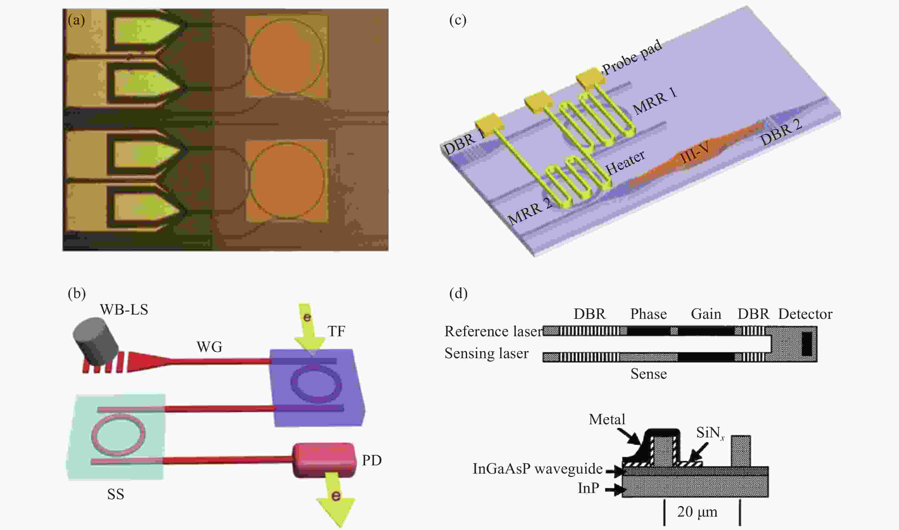
图 3 基于波导微谐振腔的片上折射率传感技术。(a)基于硅微环传感器与GeSi探测器单片集成的硅基光子集成传感器[81],光源采用片外可调谐激光器;(b)基于硅基双微环腔与GeSi探测器单片集成的电扫描硅基光子集成传感器[51],光源采用片外放大自发辐射宽带光源;(c)基于可调谐级联硅基微环谐振腔和三-五族化合物键合集成的宽带可调谐中红外激光光源,通过检测特征波长吸收信号实现气体传感[83];(d)基于InP衬底上双可调谐激光器和探测器单片集成的外差信号检测的生化传感器[84]
Figure 3. On-chip refractive index sensing technology based on waveguide-coupled micro-resonators. (a) Monolithic silicon photonic sensor with microring sensing unit and GeSi detector operating with an off-chip tunable laser [81]; (b) Monolithic silicon photonic sensor with electrically scanned dual-microring sensing unit and GeSi detector operating with an off-chip amplified spontaneous emission broadband light source [51]; (c) A broadband tunable mid-infrared laser based on tunable cascaded silicon microrings and bonded III-V active layer for gas sensing by monitoring the absorption fingerprint [83]; (d) A biochemical sensor based on heterodyne signal detection with monolithically integrated dual tunable lasers and detector on InP substrate [84]
波导型的器件在光学传感和光电探测两个方面都可以充分利用光波导沿光传输方向的延伸优势,提高光与被测物或光与光电有源材料的相互作用,从而增加传感灵敏度和探测灵敏度。硅光技术的成熟也极大地提高了相关器件的设计与工艺水平,保证了器件的较高性能。尤其是在片上光源(例如:InGaAs/Si键合集成激光器[85]、硅基外延InAs/GaAs量子点激光器[86]和全硅拉曼激光器[87])等技术引入后,可以实现波导互联的完全单片集成的光学传感检测,从而大大减小系统的质量、尺寸和成本,极大地提高芯片集成性和适用性。但是,波导型的架构也受到片上波导路由的限制,在面向并行检测的大规模阵列器件方面并没有优势,全功能芯片尺寸也较大。
-
自由空间型技术架构中光的传输不再由波导或光纤来导引,而是通过空间光路来进行光源、传感单元和探测单元的对准连接。例如:瑞士学者H. Altug等分别在2014年[88]和2018年[35]展示的基于金纳米孔阵列和介质超表面阵列的微型光传感器都是利用反射型的显微光路将微纳结构芯片和图像传感器进行组装的,由于需要物镜、二分镜等光学元件,无法获得真正意义上的单片集成检测芯片,而且存在光路对准误差、稳定性等问题。为了解决上述问题,一条思路就是利用微纳加工技术直接将光传感器制备到光探测器上;另一条思路就是在单个器件上实现光传感与光探测的双功能集成。前者中光传感器和光探测器的结构是独立的,但集成在同一块芯片上;后者中光传感器和光探测器为同一个结构。不同于波导型传感器可以通过增加波导长度来增大检测量的变化,空间型器件中不管是传感单元还是探测单元往往都与光传输方向垂直,与光相互作用的长度在微米级别,因此空间型器件一般都采用微纳光学结构来增强传感灵敏度。
-
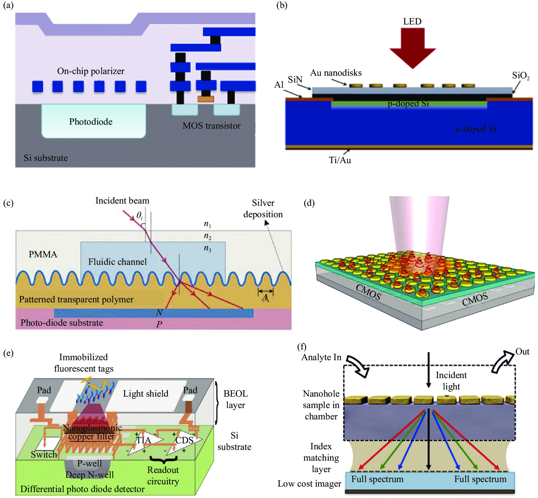
自由空间型光传感器一般通过检测被测物引起的在自由空间传输的荧光、透射与反射变化来进行物质检测,由于方便与成像结合,在生命科学和材料分析应用中较为普遍,特别是基于透射或反射光的无标记传感近年来受到广泛关注。通常会引入共振光学结构来局域光场,从而在一定程度上增强空间光与微量被测物的相互作用,表现在光谱中就是一些特定波长位置的透射或反射峰。被测物折射率实部或消光系数的变化会影响共振结构的光学特性,通过检测这些共振峰相关的幅度、波长、相位等的变化,就实现了被测物信息在光波上的信号加载,无需进行荧光标记[89]。最为常见的就是以Biacore公司为代表推出的表面等离子体共振传感器[90],通过棱镜耦合在全反射光中加载金膜表面被测物的信息。Biacore的光传感系统中用的是独立的探测器结合透镜组进行反射光的测试和输出。为了实现单片集成的光学传感检测,一个自然的想法就是将透射型的光传感器结构直接做在探测器感光区的表面,两个器件中间是透明的间隔层。实际上这种无源光学器件与有源光电器件的集成已经非常成熟,例如:手机和相机中的图像传感器就包括了一一对准的染料滤波器和硅探测器组成的千万级的像素,其中染料滤波器与硅探测器之间是由氧化硅或氮化硅形成的数微米的透明介质间隔层。这种染料滤波器与硅探测器的结合不仅成功用于图像传感器,还通过优化染料吸收波段来抑制激发光的穿透从而被用于生物样品的荧光信号检测[91]。如图4(a)所示,还可以进一步利用CMOS工艺中的金属层制备这种抑制激发光并透过荧光的滤波器或者检测手性分子的滤波器,实现全集成的CMOS检测芯片[92]。类似的,将微纳共振结构光传感器集成到探测器表面就能实现无需荧光标记的片上集成光学检测[93-94]。
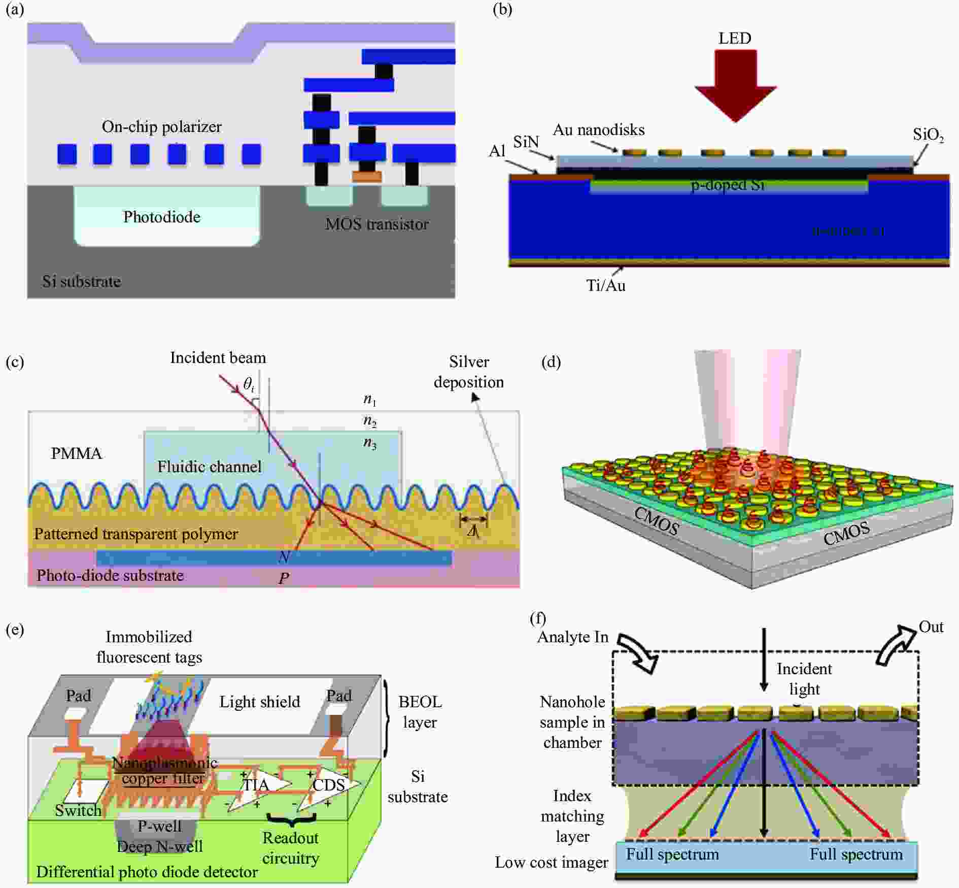
图 4 基于光传感器与光探测器垂直集成的片上光传感技术。(a)在CMOS工艺平台上集成纳米光栅偏振器和硅光电管的手性传感器[92];(b)金纳米盘阵列在硅pn结探测器表面集成的电读出光传感器[95];(c)银膜覆盖聚合物光栅在硅pn结探测器表面集成的电读出光传感器[96];(d)金纳米盘阵列在CMOS探测器表面集成的电读出光传感器[58];(e)在CMOS工艺平台上集成铜纳米光栅滤波器和硅光电管的荧光传感器[28];(f)金纳米孔阵列在CMOS图像传感器表面集成用于目标物多波长检测[103]
Figure 4. On-chip optical sensing technology based on vertically integrated optical sensor and optical detector. (a) Chiral sensor based on a nanograting polarizer integrated silicon photodiode on a CMOS platform [92]; (b) electric readout optical sensor based on a gold nanodisk array integrated silicon PN junction detector [95]; (c) electric readout optical sensor based on a silicon pn-junction detector integrated with silver film covered polymer gratings [96]; (d) electric readout optical sensor based on a gold nanodisk array integrated silicon photodiode on a CMOS platform [58]; (e) fluorescence sensor based on a copper nanograting filter integrated silicon photodiode on a CMOS platform [28]; (f) CMOS image sensor integrated with a gold nanohole array for multi-wavelength detection [103]
如图4(b)所示,瑞典学者M. P. Jonsson等人利用纳米球光刻技术将金纳米盘制备到硅PN结表面,其中金纳米盘光传感器与硅PN结探测器之间由二氧化硅和氮化硅层隔开[95]。金纳米盘支持的表面等离子体共振模式对结构表面折射率非常敏感,单波长的归一化光强变化灵敏度达到78%/RIU,即环境折射率变化量为1时会产生78%的透射光强幅值变化。通过表面修饰使得金纳米盘表面可以选择性吸附中性粒细胞,在780 nm LED光照射下对于100 μg/mL浓度的样品可以清晰地从硅探测器光电流信号中看到整个吸附过程,实现片上电信号输出的光学检测。类似的,土耳其学者B. Turker等人利用纳米压印技术在硅PN结表面制备光刻胶的纳米光栅结构并沉积薄金属膜,然后在金属光栅表面集成微流通道[96]。如图4(c)所示,金属光栅的表面等离子体共振反射大部分入射光并形成窄带透射光,共振透射波长对金属光栅表面折射率非常敏感,在2 mW功率的633 nm激光照射下观察到微流通道中反复切换去离子水和5%浓度NaCl溶液产生的微安级光电信号。
将微纳光学结构集成到CMOS芯片中是近年来的热点,基于CMOS标准工艺的材料结构和精细的加工能力,有望在CMOS平台实现更多功能的集成,并提高光学检测的兼容性和低成本应用的可行性[97-98]。英国学者D. Cumming等人利用0.35 μm的商业CMOS工艺制备出带有读出电路的硅PN探测器(图4(d)),并在探测器表面利用电子束曝光工艺制备金纳米盘结构,成功展示了水中甘油含量的实时电压信号片上输出[58]。美国学者K. Sengupta等更进一步在CMOS标准工艺的铜金属互联层制备出金属纳米结构滤波器(图4(e)),实现了基于微纳结构的集成光传感芯片的完全CMOS工艺兼容,并实验展示了对量子点探针高达48仄摩尔(10–21 mol)的检测精度[28]。常规CMOS工艺虽然提供了大规模和低成本的成熟制备技术,但硅材料的能带结构限制了其对波长大于1100 nm光谱范围光信号的探测,而大量的特异性的生化光谱信号都集中在短波红外[99],因此发展CMOS兼容的长波长光学检测芯片具有重要的应用价值。通过在硅衬底上外延锗并制备GeSi探测器并集成微纳结构光传感器,可以在近红外波段实现上述功能[100-102]。德国学者L.Augel等在硅衬底上制备p+-Si/i-Ge/n+-Ge/n+-Si探测器,在1600 nm仍有40 mA/W的光电响应度,通过进一步在表面制备金纳米孔阵列获得了表面等离子体共振调制的短波红外波段的光响应。对去离子水、乙醇和异丙醇溶液进行光电流检测,其器件优值达到16,为前述技术思想展示了一个可行的器件原型[102]。
在微纳光学传感器与探测器集成的基础上,进一步将微纳光学传感器与探测器阵列进行集成,将提供高通量检测、多目标物同时检测和光谱检测的能力。如果能将相关技术基于成熟的CMOS平台实现,有利于更广泛的应用。加拿大学者O. Yadid-Pecht等通过在CMOS图像传感器上不同像素位置分别集成两类不同滤波波长的染料滤波器,实现了水生环境中叶绿素和彩色溶解有机物荧光信号的同时检测[104]。美国学者N. C. Lindquist等在CMOS图像传感器上集成金纳米孔阵列和微流通道,其中金纳米孔阵列将不同波长的光衍射到图像传感器上的不同像素位置(图4(f)),通过监测某个波长强度随被测物的变化就能实现传感功能,折射率传感精度达到5×10⁻⁴ RIU[103]。
-
不管是引言部分介绍的依赖外部检测设备的光传感技术,还是波导型光传感技术,以及2.1节介绍的光传感器与光探测器垂直集成的自由空间型光传感技术,光信号对被测物的感知和光信号的电转换都发生在不同器件结构中。实际上,光电探测的有源器件与光传感的无源器件可以融合到单一器件结构中,即获得光学传感信号的原位光电探测。基于光探测的传感应用并不少见,例如:通过调节门电压来控制探测器中不同波长的吸收深度,从而通过扫电压获取被测物的光谱[105-106],或者利用多孔结构对气体的强吸附性以及肖特基势垒对表界面的敏感性在铂硅-多孔硅探测器上开发的气体传感应用[107],甚至直接将微流通道集成在探测器感光区表面展示对乙醇、异丙醇和去离子水的区分[108]。为了提高光学传感的灵敏度,通常需要增大光场与被测物的空间重叠,基于金属纳米结构的表面等离子体共振模式具有很高的表面光场局域,因此被广泛应用于光学传感研究中,如2.1节中介绍的大多数例子。同时,光探测器必然需要金属电极来实现电信号的输出,能否将光传感的金属纳米结构同时用作光探测器的电极,实现单一结构的双功能化,是一个具有新意的想法,对于提高集成度以及利用微纳光学结构同时增强传感与探测都具有积极作用。
基于棱镜耦合的表面等离子体共振传感技术已经商业化,在生化研究中得到广泛应用[90]。然而,其对精密机械控制系统或高分辨光谱仪的依赖造成了其检测系统高昂的价格。美国学者M. A. Baldo等提出利用金属-有源材料-金属三层结构代替棱镜耦合体系中的金膜(图5(a)),从而使得外表面金属层上生物分子的选择性吸附引起的吸收光谱的变化影响到有源材料层的光电转换过程,从而实现了生物信息的直接片上电读出,摆脱了对机械调节系统和光谱分析系统的依赖[109]。实验中采用1 mW功率的670 nm激光对中性粒细胞的检测限达到了4 μg/cm2。但是该方案中双金属层的结构会影响光的透射和倏逝波的产生,因此限制了器件的性能。为此,韩国学者B. Park等提出了改进方案,将底层金属换成ITO,基于聚合物光伏有源材料在可见光波段展现了对生物素-链霉亲和素结合过程的检测[110]。这种方案中棱镜的使用会限制整个检测系统的进一步小型化。近年来各种微纳结构光传感层出不穷,入射光与微纳结构中光场模式的耦合可以通过布洛赫波矢和散射等来实现,解除了对棱镜耦合方式的依赖,被认为有望成为小型化和阵列化传感器的潜在方案[45,79,111-112]。如图5(b)所示,加拿大学者M. Meunier等在硅衬底上依次沉积二氧化硅和金膜构成MOS探测器,并在金膜上制备纳米孔阵列结构用于可见光波段的电压型光传感[113]。到达硅有源层的光需要穿过金纳米孔阵列,因此探测器的响应受到金纳米孔阵列结构透射光谱调控,进而能响应器件表面的生物分子。实验中对于0.7%的乙醇浓度变化获得了毫伏级的输出电信号,折射率灵敏度达到4×10⁻⁵ RIU。

图 5 基于光学传感原位探测的片上光传感技术。(a)棱镜耦合的金属-半导体-金属架构的光传感器[109];(b)纳米孔阵列集成的金属-绝缘层-半导体架构的光传感器[113];(c)金膜覆盖硅纳米光栅的肖特基结架构的光传感器[54];(d)金纳米颗粒覆盖的Au-IGZO-Au光电导架构的光传感器[121];(e)氧化钒集成金膜覆盖硅纳米光栅的热阻型中红外波段光传感器[53];(f)氧化锂钽与超材料吸收器集成的热释电型气体传感器[122];(g) ZnO和金属纳米盘阵列集成的热释电型中远红外波段光传感器[123];(h)金纳米棒阵列与液态镓铟合金构建的隧道结光传感器[124]
Figure 5. On-chip optical sensing technology with in-situ photodetection. (a) Optical sensor based on a prism-coupled metal-semiconductor-metal multilayer [109]; (b) Optical sensor based on nanohole array integrated metal-insulator-semiconductor multilayer [113]; (c) Optical sensor based on gold film covered silicon nanogratings [54]; (d) Optical sensor based on gold nanoparticles covered Au-IGZO-Au photoconductive diode [121]; (e) Optical sensor based on a vanadium oxide bolometer integrated with gold film covered silicon nanogratings [53]; (f) Optical sensor based on a pyroelectric detector integrated with lithium tantalate and metamaterial absorber [122]; (g) Optical sensor based on a pyroelectric detector integrated with ZnO and metal nanodisk array [123]; (h) Optical sensor based on a tunnel junction consisting of gold nanorod array and liquid gallium indium [124]
肖特基探测器的光电响应与金属结构的光吸收密切联系,将肖特基结一侧的金属制备成高灵敏的光学传感结构,就有望获得光传感信号的原位读出。不仅如此,金属纳米结构的光场局域和共振吸收对于光传感和光探测都具有显著增强作用,且肖特基探测器有望突破有源材料带间跃迁的波长限制实现更长波段的光学传感检测[114]。如图5(c)所示,暨南大学陈沁等利用步进式光刻技术制备了金膜覆盖的浅刻蚀硅光栅结构,光栅周期这种表面等离子体共振结构具有表面局域的光场和较低的辐射损耗,优化结构理论上可以获得近100%的共振光吸收且线宽仅10 nm,非常有利于光电流传感,而金-硅肖特基探测器结构使其工作范围覆盖700~1700 nm。针对酒精溶液浓度进行测试,光电传感灵敏度超过3000 mA/W/RIU,折射率检测限达到10−5~10−6 RIU量级[54]。日本学者T. Kan等基于金-硅肖特基结,分别采用在金膜[115]、光刻胶[116]和硅[117-119]上制备光栅的方式发展了类似的电读出光学传感器,其中光栅周期超过了3 μm,因此需要基于高阶共振模式进行传感测试。他们将该器件放在旋转台上,通过扫描旋转角获得了精度为10 nm左右的近红外波段光谱测量[115]。进一步,他们通过减薄硅衬底将器件做成悬臂梁结构,并利于声波驱动悬臂梁进行摆动,基于高阶共振模式来扫描光谱,展示了1200~1400 nm的光谱测试[119]。通过在器件表面集成微流通道,他们也展示了水和酒精溶液对光电流的影响[116-118]。这类基于金属纳米结构的肖特基探测器虽然具有很高的光学传感灵敏度,但由于探测器本身的量子效率很低,最终的器件性能还是受限于信噪比。意大利学者D. Sammito等报道了一种金属纳米光栅集成的GaAs基高电子迁移率光子晶体管[120],通过在常规高电子迁移率晶体管的沟道层上方制备金属光栅并形成肖特基结作为栅极,使得该器件可以具有光响应,尤其是在栅控下沟通中二维电子气接近耗尽时光电响应非常灵敏。金属光栅的表面等离子体共振对表面介电环境非常敏感,因此利用沟通电导率的变化可以直接检测器件表面被测物的变化。如图5(d)所示,美国学者S. J. Kim等实验展示了这类场效应管的生物传感应用,通过在Au-InGaZnO-Au光电导探测器的感光区表面制备金纳米颗粒,利用栅压下金纳米颗粒吸收光后通过Au/InGaZnO肖特基势垒注入到导电通道中的电流实现光电探测信号的放大,进而高灵敏地感知金纳米颗粒表面的生化反应[121]。他们实验发现这种方案将糖聚合物间结合的检测精度提高两个数量级,实现皮摩尔凝集素的检测。其理论分析也支持了实验中的发现,并预计这种技术方案对伴刀豆血球凝集素有望实现对0.4 pg/mL的检测限[125]。
对于气体传感而言,丰富的气体分子指纹信息基本落在中远红外,通过将微纳光学传感结构与测辐射热仪或热释电探测器等集成,就可以将上述技术思想在中远红外波段实现[53,122,126]。暨南大学陈沁等提出在硅光栅表面沉积二氧化钒和金膜的器件结构(图5(e)),入射光与表面等离子体模式发生谐振并被金膜吸收并转换成热,使得二氧化钒层的电阻升高,形成电信号。这种表面光场强局域、高品质因子和高光吸收的表面等离子体共振模式将有效地将器件表面被测物的变化转换成片上电信号输出,对CO2的检测精度达到100 ppm[53]。不仅如此,通过将器件阵列化并结合压缩感知光谱重构算法,还能实现片上高精度的光谱检测。华中科技大学易飞等将氧化锂钽与超材料吸收器集成制备了窄带热释电探测器(图5(f)),响应波长由超材料吸收器决定,通过调节超材料吸收器的结构并形成阵列,可以实现不同波长位置、不同气体分子传感信号的同时检测,他们实验中展示了对一氧化碳(4.67 μm)和二氧化硫(7.35 μm)混合气体中不同气体含量的检测[122,126]。日本学者T. Naogo等基于ZnO热释电材料和表面等离子体共振也制作了品质因子超过70的窄带中远红外探测器(图5(g)),可用于气体探测[123]。此外,在器件表面制备气体选择性吸附材料将显著增加传感灵敏度[23],例如:红外光与气体分子的作用强度在金属氧化物框架结构和表面等离子体共振的共同作用下增强了8000倍[53]。
前述工作都是将传感器与探测器进行集成,光源依然需要外部引入。如果能将光源集成起来,无疑将获得更高的集成度。如图5(h)所示,浙江大学王攀等利用金纳米棒阵列与液态镓铟合金电极及其之间修饰的组氨酸反应物构建隧道结来检测氧化还原反应的动力学过程[124]。对该结构施加偏压,非弹性隧穿电子激发金纳米棒的等离子体共振并随后以光的形式辐射出去,而弹性隧穿电子产生的热电子参与到隧道结处的氧化还原反应。因此,隧道结处的氧化还原反应会影响金纳米棒的表面等离子体共振辐射,通过检测辐射强度就可以直接获得氧化还原反应的信息。虽然实验中的辐射主要在近红外波段(~850 nm),但其在红光区的能量分布也为基于人眼的比色传感提供了一定基础,从而获得高度的便携性。他们还发现在隧道结处通入反应气体后,金纳米棒辐射形成的光信号和隧道结的隧穿电流信号都具备时间相关性,表现出了与神经突触类似的行为,具有非易失性的感知能力[127]。
可以看到,不管是2.1节介绍的光传感器与光探测器垂直集成技术方案,还是2.2节介绍的光学传感原位探测技术方案,都有效地获得了片上直接电信号输出的光学传感检测。2.1节方案中高灵敏的光学传感来源于微纳光学结构的强局域共振模式,同时这些结构通过透射和衍射等光学效应将携带被测物信息的光学信号传递给有源光电材料,从而实现传感器与探测器的单片集成,是一种简单易行的技术方案。由于光传感器与光探测器在结构上相对独立,材料和结构选择的限制更少,可以分别进行优化。此外,这种方案还可以扩展到更多的光电材料平台,例如:三-五族化合物半导体或钙钛矿等,不仅可以进一步扩展工作波段,还可能获得光源的集成,实现检测系统的单片全集成[52]。2.2节方案中微纳金属结构通常同时用于光传感与光探测功能的实现,器件更加紧凑,但也在一定程度上限制了功能优化的余地。不过微纳光学结构可以同时增强光传感与光探测,不仅提高传感灵敏度,还获得检测光谱范围扩展和场效应放大等新功能,无疑增强了该方案的检测功能并提高其适用性。自由空间型器件中光的传输方向往往与被测物和有源光电材料层垂直,因此相互作用距离很有限,不能类似波导型器件那样通过增加器件长度来提高器件性能。不管是上述哪种技术方案,关键在于如何利用微纳光学结构增强光传感与光探测,并有效实现单片集成。自由空间型可以充分利用二维空间的光场分布,具有非常好的空间扩展性,用以实现大通量并行检测或多目标物同时检测,尤其是与千万级像素的CMOS图像传感器技术结合,极大地提升检测能力与多功能集成。
-
近10年来,为了应对现场快检和轻载荷平台检测的技术需求,光学传感检测技术呈现出高集成化、网络化、智能化和无人化的发展趋势,片上集成光学传感检测技术取得了重要的发展。不管是波导型还是自由空间型的片上集成光传感器,相比于光源、光探测器和光传感器等分立单元构成的光传感检测系统,展现了小型化、阵列化和多功能化的巨大优势。波导型通常具有更长的光与被测物的作用距离,有助于提高检测精度;自由空间型更加易于阵列化,尤其是和千万级像素的CMOS图像传感器结合极大地扩展了检测通量和多功能扩展空间。单片集成的主要技术途径包括:(1)将分立单元器件通过键合、沉积或外延逐一集成到共同基底;(2)在单一结构中融合分立器件的功能。此外,片上光谱仪也是便携式光学检测技术的重要分支,近期已有大量优秀的综述[18,19,128-129],文中不再赘述。为了提高小型化器件的检测精度,微型谐振腔或各种共振结构都可以集成到器件中进行光场(幅度、频率、相位等)调控,获得强局域光场分布、窄线宽共振、临界耦合态等来增强光与被测物的相互作用或放大光传感信号。这些优化手段使得片上集成光学传感检测技术在芯片化的同时,保持了较高的检测性能,例如:折射率变化检测限达到10−6~10−7 RIU;气体浓度检测限达到1~10 ppm;生物分子检测限达到皮摩尔;量子点探针检测限更是达到了50仄摩尔以下。这些光学传感检测芯片如果搭载到手机、无人机等移动端平台,结合物联网、云计算和大数据技术,将极大地提高检测和实时监控的能力,在食品安全、智慧农业、环境监测、重大疫情防控和公共安全等领域具有重要的应用潜力。
片上集成光学传感检测技术取得了巨大进步,但依然存在一些问题。(1)光源集成的问题。目前探测器和传感器的集成难度不大,最困难的是光源的片上集成。高质量的激光光源都依赖复杂的外延工艺和昂贵的化合物半导体,对衬底的要求非常严格,因此单片集成光源、探测器和传感器往往造成多方面的妥协,导致总体性能的下降。键合技术是目前硅基光子中最成熟的光源集成技术,异质外延技术的发展有望提供另一种技术途径。低成本的LED光源也是片上光传感检测技术集成光源的选择之一,microLED的巨量转移技术有望用于这类宽带光源的片上集成。(2) CMOS工艺兼容问题。相比于化合物材料,硅材料器件工艺成熟,价格低廉,甚至被用作可抛弃的一次性检测器。CMOS图像传感器因其千万级像素是优异的高通量检测平台,目前已有在CMOS工艺金属层中插入纳米光学结构来做荧光滤波的尝试,但大多数还是依靠后工艺将微纳结构传感器等集成到CMOS图像传感器上。如何从器件设计、工艺优化等不同角度解决兼容性的问题,实现完全的CMOS兼容,将是未来研究的重要部分。(3)智能检测技术。不可否认小型化尤其是芯片化之后光学传感检测技术的性能相比于分立单元组成的大型检测设备有明显下降。最近,这类微型器件在硬件上的固有不足一定程度通过压缩感知、神经网络等人工智能算法得到了弥补,例如:微型光谱仪通过压缩感知算法实现了相比于传统光栅光谱仪高四倍的光谱信息提取效率[112],而且通过优化还能获得接近甚至超过传统光谱仪的光谱分辨率[53]。因此,智能化、网络化将有效推动片上集成光学传感检测技术的应用。
Research progress of on-chip integrated optical sensing technology (Invited)
-
摘要: 光学传感检测技术因具有精度高、低延时和可成像等优势而得到广泛应用。随着大数据和物联网等信息技术的迅速发展,对检测平台小型化和便携性的需求日益迫切。为了克服现有技术对大型专用设备的依赖,提高对现场快检、轻载荷平台等应用场景的适用性,近年来,基于微纳光学的片上集成光学传感检测技术受到了极大关注。通过集成光源、光学传感单元与光电探测单元、以及发展片上光色散等技术,可以有效地实现光学传感信号提取和光电信号转换的片上集成,从而实现系统的微型化和多功能集成。文中介绍了相关技术原理和技术发展现状,分析了现有技术的优缺点,讨论并总结了未来的发展方向和应用前景。Abstract: Optical sensing technology has been widely used because of its advantages of high precision, low delay and imaging. With the rapid development of information technology such as big data and Internet of things, the demand for miniaturization and portability of optical detection and inspection platform is becoming more and more urgent. In order to overcome the dependence on large-scale special equipment and improve the applicability of on-site rapid detection and light-load platform application scenarios, in recent years on-chip integrated optical sensing technology has attracted great attention. With the integration of optical source, optical sensing and photoelectric detection units, as well as the development of on-chip light dispersion technology, the on-chip integration of optical sensing signal extraction and photoelectric signal conversion can be effectively realized, which contributes to the realization of the miniaturization and multi-functional integration. The relevant technical principles and technology development status were introduced, the pros and cons of the existing techniques were discussed, and the future development direction and application prospects were summarized.
-
Key words:
- optical sensing /
- photodetection /
- optical waveguide /
- integrated optics /
- lab on a chip
-
图 1 片上集成光学传感检测技术路线。(a)波导型包括:(a1)基于波导模式的指纹光吸收传感器[55];(a2)基于波导微谐振腔的折射率传感器[57]。(b)自由空间型包括:(b1)低通滤波器集成的荧光计[52];(b2)微纳谐振结构垂直集成的探测器[58];(b3)具有原位光电探测的光传感器[54]
Figure 1. Route of chip-integrated optical sensing technology. (a) The waveguide type includes: (a1) Fingerprint light absorption waveguide sensor [55]; (a2) Refractive index sensor based on waveguide microresonator [57]. (b) The free-space type includes: (b1) Low-pass filter integrated fluorometer [52]; (b2) Micro/nano-resonant structure vertically integrated detector [58]; (b3) Optical sensor with in-situ photodetection [54]
图 2 基于波导模式非色散光吸收的片上光传感技术。(a) GeSbS螺旋光传感波导与PbTe探测器单片集成的气体传感器[65];(b) CaF2衬底上单片集成硅光传感波导与石墨烯波导探测器的气体传感器[66];(c) GaSb衬底上外延制备的带间级联激光器与沉积工艺制备的As2Se3光传感波导的单片集成[67];(d) InP衬底上量子级联激光器、量子级联探测器和表面等离子体传感波导单片集成的溶液传感器[55];(e)玻璃衬底上基于Al-AlOx-Au隧道结的宽带光源与探测器的单片集成,两者间由表面等离子体波导连接[56];(f)在聚合物柔性基底上单片集成InGaAs探测器和硫系玻璃光传感波导[68]
Figure 2. On-chip optical sensing technology based on non-dispersive light absorption of the waveguide mode. (a) Monolithic gas sensor with GeSbS spiral optical sensing waveguide and PbTe waveguide detector [65]; (b) Monolithic gas sensor with silicon optical sensing waveguide and graphene waveguide detector on CaF2 substrate [66]; (c) Monolithic integration of epitaxially grown inter-band cascade laser and deposited As2Se3 optical sensing waveguide on GaSb substrate [67]; (d) Monolithic sensor with quantum cascade laser, quantum cascade detector and surface plasmon sensing waveguide on InP substrate [55]; (e) Monolithic integration of broadband light source and detector based on Al-AlOx-Au tunnel junction on glass substrate, which are connected by surface plasmon waveguide [56]; (f) Monolithic integration of InGaAs detector and chalcogenide glass optical sensing waveguide on polymer flexible substrate [68]
图 3 基于波导微谐振腔的片上折射率传感技术。(a)基于硅微环传感器与GeSi探测器单片集成的硅基光子集成传感器[81],光源采用片外可调谐激光器;(b)基于硅基双微环腔与GeSi探测器单片集成的电扫描硅基光子集成传感器[51],光源采用片外放大自发辐射宽带光源;(c)基于可调谐级联硅基微环谐振腔和三-五族化合物键合集成的宽带可调谐中红外激光光源,通过检测特征波长吸收信号实现气体传感[83];(d)基于InP衬底上双可调谐激光器和探测器单片集成的外差信号检测的生化传感器[84]
Figure 3. On-chip refractive index sensing technology based on waveguide-coupled micro-resonators. (a) Monolithic silicon photonic sensor with microring sensing unit and GeSi detector operating with an off-chip tunable laser [81]; (b) Monolithic silicon photonic sensor with electrically scanned dual-microring sensing unit and GeSi detector operating with an off-chip amplified spontaneous emission broadband light source [51]; (c) A broadband tunable mid-infrared laser based on tunable cascaded silicon microrings and bonded III-V active layer for gas sensing by monitoring the absorption fingerprint [83]; (d) A biochemical sensor based on heterodyne signal detection with monolithically integrated dual tunable lasers and detector on InP substrate [84]
图 4 基于光传感器与光探测器垂直集成的片上光传感技术。(a)在CMOS工艺平台上集成纳米光栅偏振器和硅光电管的手性传感器[92];(b)金纳米盘阵列在硅pn结探测器表面集成的电读出光传感器[95];(c)银膜覆盖聚合物光栅在硅pn结探测器表面集成的电读出光传感器[96];(d)金纳米盘阵列在CMOS探测器表面集成的电读出光传感器[58];(e)在CMOS工艺平台上集成铜纳米光栅滤波器和硅光电管的荧光传感器[28];(f)金纳米孔阵列在CMOS图像传感器表面集成用于目标物多波长检测[103]
Figure 4. On-chip optical sensing technology based on vertically integrated optical sensor and optical detector. (a) Chiral sensor based on a nanograting polarizer integrated silicon photodiode on a CMOS platform [92]; (b) electric readout optical sensor based on a gold nanodisk array integrated silicon PN junction detector [95]; (c) electric readout optical sensor based on a silicon pn-junction detector integrated with silver film covered polymer gratings [96]; (d) electric readout optical sensor based on a gold nanodisk array integrated silicon photodiode on a CMOS platform [58]; (e) fluorescence sensor based on a copper nanograting filter integrated silicon photodiode on a CMOS platform [28]; (f) CMOS image sensor integrated with a gold nanohole array for multi-wavelength detection [103]
图 5 基于光学传感原位探测的片上光传感技术。(a)棱镜耦合的金属-半导体-金属架构的光传感器[109];(b)纳米孔阵列集成的金属-绝缘层-半导体架构的光传感器[113];(c)金膜覆盖硅纳米光栅的肖特基结架构的光传感器[54];(d)金纳米颗粒覆盖的Au-IGZO-Au光电导架构的光传感器[121];(e)氧化钒集成金膜覆盖硅纳米光栅的热阻型中红外波段光传感器[53];(f)氧化锂钽与超材料吸收器集成的热释电型气体传感器[122];(g) ZnO和金属纳米盘阵列集成的热释电型中远红外波段光传感器[123];(h)金纳米棒阵列与液态镓铟合金构建的隧道结光传感器[124]
Figure 5. On-chip optical sensing technology with in-situ photodetection. (a) Optical sensor based on a prism-coupled metal-semiconductor-metal multilayer [109]; (b) Optical sensor based on nanohole array integrated metal-insulator-semiconductor multilayer [113]; (c) Optical sensor based on gold film covered silicon nanogratings [54]; (d) Optical sensor based on gold nanoparticles covered Au-IGZO-Au photoconductive diode [121]; (e) Optical sensor based on a vanadium oxide bolometer integrated with gold film covered silicon nanogratings [53]; (f) Optical sensor based on a pyroelectric detector integrated with lithium tantalate and metamaterial absorber [122]; (g) Optical sensor based on a pyroelectric detector integrated with ZnO and metal nanodisk array [123]; (h) Optical sensor based on a tunnel junction consisting of gold nanorod array and liquid gallium indium [124]
-
[1] Borisov S M, Wolfbeis O S. Optical biosensors [J]. Chemical Reviews, 2008, 108(2): 423-461. doi: 10.1021/cr068105t [2] Singh V, Hu J J, Agarwal A M, et al. Integrated optical sensors [J]. IEEE Photonics Journal, 2012, 4(2): 638-641. doi: 10.1109/JPHOT.2012.2192721 [3] Yan X, Li H X, Su X G. Review of optical sensors for pesticides [J]. Trac-Trends in Analytical Chemistry, 2018, 103: 1-20. doi: 10.1016/j.trac.2018.03.004 [4] Wang Q, Zhao W M. Optical methods of antibiotic residues detections: A comprehensive review [J]. Sensors and Actuators B-Chemical, 2018, 269: 238-256. [5] Salek-Maghsoudi A, Vakhshiteh F, Torabi R, et al. Recent advances in biosensor technology in assessment of early diabetes biomarkers [J]. Biosensors & Bioelectronics, 2018, 99: 122-135. [6] Khansili N, Rattu G, Krishna P M. Label-free optical biosensors for food and biological sensor applications [J]. Sensors and Actuators B-Chemical, 2018, 265: 35-49. doi: 10.1016/j.snb.2018.03.004 [7] Gao M K, Gao Y H, Tian M S, et al. Research on the application of optical sensor in quality and safety of agricultural products [J]. Chinese Journal of Analysis Laboratory, 2020, 39(10): 1225-1232. (in Chinese) [8] Tariq A, Baydoun J, Remy C, et al. Fluorescent molecular probe based optical fiber sensor dedicated to pH measurement of concrete [J]. Sensors and Actuators B-Chemical, 2021, 327: 128906. doi: 10.1016/j.snb.2020.128906 [9] Simsir E A, Erdemir S, Tabakci M, et al. Nano-scale selective and sensitive optical sensor for metronidazole based on fluorescence quenching: 1H-Phenanthro[9, 10-d]imidazolyl-calix[4]arene fluorescent probe [J]. Analytica Chimica Acta, 2021, 1162: 338494. doi: 10.1016/j.aca.2021.338494 [10] Lin D, Zheng Z C, Wang Q W, et al. Label-free optical sensor based on red blood cells laser tweezers Raman spectroscopy analysis for ABO blood typing [J]. Optics Express, 2016, 24(21): 24750-24759. doi: 10.1364/OE.24.024750 [11] Shvalya V, Filipic G, Zavasnik J, et al. Surface-enhanced Raman spectroscopy for chemical and biological sensing using nanoplasmonics: The relevance of interparticle spacing and surface morphology [J]. Applied Physics Reviews, 2020, 7(3): 031307. doi: 10.1063/5.0015246 [12] Adao T, Hruska J, Padua L, et al. Hyperspectral imaging: A review on UAV-based sensors, data processing and applications for agriculture and forestry [J]. Remote Sensing, 2017, 9(11): 1110. doi: 10.3390/rs9111110 [13] Mahlein A K, Kuska M T, Behmann J, et al. Hyperspectral sensors and imaging technologies in phytopathology: State of the art [J]. Annual Review of Phytopathology, 2018, 56: 535-558. doi: 10.1146/annurev-phyto-080417-050100 [14] Tokel O, Inci F, Demirci U. Advances in plasmonic technologies for point of care applications [J]. Chemical Reviews, 2014, 114(11): 5728-5752. doi: 10.1021/cr4000623 [15] Lopez G A, Estevez M C, Soler M, et al. Recent advances in nanoplasmonic biosensors: Applications and lab-on-a-chip integration [J]. Nanophotonics, 2017, 6(1): 123-136. doi: 10.1515/nanoph-2016-0101 [16] Geng Z X, Zhang X, Fan Z Y, et al. Recent progress in optical biosensors based on smartphone platforms [J]. Sensors, 2017, 17(11): 2449. doi: 10.3390/s17112449 [17] Liang Y, Xu T. Integrated miniature plasmonic nanostructure sensors [J]. Physics, 2019, 48(1): 22-28. (in Chinese) [18] Wang W P, Jin L. Research progress of on-chip spectrometer based on the silicon photonics platform [J]. Spectroscopy and Spectral Analysis, 2020, 40(2): 333-342. (in Chinese) [19] Yang Z Y, Albrow-Owen T, Cai W W, et al. Miniaturization of optical spectrometers [J]. Science, 2021, 371(6528): eabe0722. doi: 10.1126/science.abe0722 [20] Zhang L, Pan J, Zhang Z, et al. Ultrasensitive skin-like wearable optical sensors based on glass micro/nanofibers [J]. Opto-Electronic Advances, 2020, 3(3): 190022. [21] Zheng Y, Wu Z F, Shum P P, et al. Sensing and lasing applications of whispering gallery mode microresonators [J]. Opto-Electronic Advances, 2018, 1(9): 180085. [22] Hao Y F, Feng Z Y, Han C, et al. Application of high sensitive detection sensor chip in detection of brain glioma disease [J]. Infrared and Laser Engineering, 2021, 50(8): 20210279. (in Chinese) [23] Hasan D, Lee C. Hybrid metamaterial absorber platform for sensing of CO2 gas at mid-IR [J]. Advanced Science, 2018, 5(5): 1700581. doi: 10.1002/advs.201700581 [24] Visser D, Choudhury B D, Krasovska I, et al. Refractive index sensing in the visible/NIR spectrum using silicon nanopillar arrays [J]. Optics Express, 2017, 25(11): 12171-12181. doi: 10.1364/OE.25.012171 [25] Im H, Sutherland J N, Maynard J A, et al. Nanohole-based surface plasmon resonance instruments with improved spectral resolution quantify a broad range of antibody-ligand binding kinetics [J]. Analytical Chemistry, 2012, 84(4): 1941-1947. doi: 10.1021/ac300070t [26] Armani D K, Kippenberg T J, Spillane S M, et al. Ultra-high-Q toroid microcavity on a chip [J]. Nature, 2003, 421(6926): 925-928. doi: 10.1038/nature01371 [27] Rosenblum S, Lovsky Y, Arazi L, et al. Cavity ring-up spectroscopy for ultrafast sensing with optical microresonators [J]. Nature Communications, 2015, 6: 6788. doi: 10.1038/ncomms7788 [28] Hong L Y, Li H, Yang H, et al. Fully integrated fluorescence biosensors on-chip employing multi-functional nanoplasmonic optical structures in CMOS [J]. IEEE Journal of Solid-State Circuits, 2017, 52(9): 2388-2406. doi: 10.1109/JSSC.2017.2712612 [29] Zhu J G, Ozdemir S K, Xiao Y F, et al. On-chip single nanoparticle detection and sizing by mode splitting in an ultrahigh-Q microresonator [J]. Nature Photonics, 2010, 4(1): 46-49. doi: 10.1038/nphoton.2009.237 [30] Jin T N, Lin H Y G, Lin P T. Monolithically integrated Si-on-AIN mid-infrared photonic chips for real-time and label-free chemical sensing [J]. ACS Applied Materials & Interfaces, 2017, 9(49): 42905-42911. [31] Rodriguez-Saona L, Aykas D P, Borba K R, et al. Miniaturization of optical sensors and their potential for high-throughput screening of foods [J]. Current Opinion in Food Science, 2020, 31: 136-150. doi: 10.1016/j.cofs.2020.04.008 [32] Johann S, Mansurova M, Kohlhoff H, et al. Wireless mobile sensor device for in-situ measurements with multiple fluorescent sensors [C]//IEEE Sensors Conference, 2018: 1067-1070. [33] Zhang J L, Khan I, Zhang Q W, et al. Lipopolysaccharides detection on a grating-coupled surface plasmon resonance smartphone biosensor [J]. Biosensors & Bioelectronics, 2018, 99: 312-317. [34] Xu X Y, Chen W J, Zhao G M, et al. Wireless whispering-gallery-mode sensor for thermal sensing and aerial mapping [J]. Light-Science & Applications, 2018, 7: 62. [35] Tittl A, Leitis A, Liu M K, et al. Imaging-based molecular barcoding with pixelated dielectric metasurfaces [J]. Science, 2018, 360(6393): 1105. doi: 10.1126/science.aas9768 [36] Estevez M C, Alvarez M, Lechuga L M. Integrated optical devices for lab-on-a-chip biosensing applications [J]. Laser & Photonics Reviews, 2012, 6(4): 463-487. [37] Wang H, Zhang Y L, Wang W, et al. On-chip laser processing for the development of multifunctional microfluidic chips [J]. Laser & Photonics Reviews, 2017, 11(2): 1600116. [38] Yavas O, Svedendahl M, Dobosz P, et al. On-a-chip biosensing based on all-dielectric nanoresonators [J]. Nano Letters, 2017, 17(7): 4421-4426. doi: 10.1021/acs.nanolett.7b01518 [39] Brown C, Goncharov A, Ballard Z S, et al. Neural network-based on-chip spectroscopy using a scalable plasmonic encoder [J]. ACS Nano, 2021, 15(4): 6305-6315. doi: 10.1021/acsnano.1c00079 [40] Garcia-Meca C, Lechago S, Brimont A, et al. On-chip wireless silicon photonics: From reconfigurable interconnects to lab-on-chip devices [J]. Light-Science & Applications, 2017, 6(9): e17053. [41] Lin P T, Kwok S W, Lin H Y G, et al. Mid-infrared spectrometer using opto-nanofluidic slot-waveguide for label-free on-chip chemical sensing [J]. Nano Letters, 2014, 14(1): 231-238. doi: 10.1021/nl403817z [42] Acimovic S S, Sipova H, Emilsson G, et al. Superior LSPR substrates based on electromagnetic decoupling for on-a-chip high-throughput label-free biosensing [J]. Light-Science & Applications, 2017, 6(8): e17042. [43] Lu C H, Shih T S, Shih P C, et al. Finger-powered agglutination lab chip with CMOS image sensing for rapid point-of-care diagnosis applications [J]. Lab on a Chip, 2020, 20(2): 424-433. doi: 10.1039/C9LC00961B [44] Zhang Y, Wang G, Yang L, et al. Recent advances in gold nanostructures based biosensing and bioimaging [J]. Coordination Chemistry Reviews, 2018, 370: 1-21. doi: 10.1016/j.ccr.2018.05.005 [45] Blanchard-Dionne A P, Meunier M. Sensing with periodic nanohole arrays [J]. Advances in Optics and Photonics, 2017, 9(4): 891-940. doi: 10.1364/AOP.9.000891 [46] Brolo A G. Plasmonics for future biosensors [J]. Nature Photonics, 2012, 6(11): 709-713. doi: 10.1038/nphoton.2012.266 [47] Anker J N, Hall W P, Lyandres O, et al. Biosensing with plasmonic nanosensors [J]. Nature Materials, 2008, 7(6): 442-453. doi: 10.1038/nmat2162 [48] Zanchetta G, Lanfranco R, Giavazzi F, et al. Emerging applications of label-free optical biosensors [J]. Nanophotonics, 2017, 6(4): 627-645. doi: 10.1515/nanoph-2016-0158 [49] Xu Y, Bian J, Zhang W H. Principles and processes of nanometric localized-surface-plasmonic optical sensors [J]. Laser & Optoelectronics Progress, 2019, 56(20): 202407. (in Chinese) [50] Ma Y M, Dong B W, Lee C K. Progress of infrared guided-wave nanophotonic sensors and devices [J]. Nano Convergence, 2020, 7: 12. doi: 10.1186/s40580-020-00222-x [51] Song J F, Luo X S, Kee J S, et al. Silicon-based optoelectronic integrated circuit for label-free bio/chemical sensor [J]. Optics Express, 2013, 21(15): 17931-17940. doi: 10.1364/OE.21.017931 [52] Dandin M, Abshire P, Smela E. Optical filtering technologies for integrated fluorescence sensors [J]. Lab on a Chip, 2007, 7(8): 955-977. doi: 10.1039/b704008c [53] Chen Q, Liang L, Zheng Q L, et al. On-chip readout plasmonic mid-IR gas sensor [J]. Opto-Electronic Advances, 2020, 3(7): 07190040. [54] Wen L, Liang L, Yang X G, et al. Multiband and ultrahigh figure-of-merit nanoplasmonic sensing with direct electrica readout in Au-Si nanojunctions [J]. ACS Nano, 2019, 13(6): 6963-6972. doi: 10.1021/acsnano.9b01914 [55] Schwarz B, Reininger P, Ristanic D, et al. Monolithically integrated mid-infrared lab-on-a-chip using plasmonics and quantum cascade structures [J]. Nature Communications, 2014, 5: 4085. doi: 10.1038/ncomms5085 [56] Du W, Wang T, Chu H S, et al. Highly efficient on-chip direct electronic-plasmonic transducers [J]. Nature Photonics, 2017, 11(10): 623-627. doi: 10.1038/s41566-017-0003-5 [57] Singh R, Su P, Kimerling L, et al. Towards on-chip mid infrared photonic aerosol spectroscopy [J]. Applied Physics Letters, 2018, 113(23): 231107. doi: 10.1063/1.5058694 [58] Shakoor A, Cheah B C, Hao D, et al. Plasmonic sensor monolithically integrated with a CMOS photodiode [J]. ACS Photonics, 2016, 3(10): 1926-1933. doi: 10.1021/acsphotonics.6b00442 [59] Zhao Y, Zhao J, Zhao Q. Review of no-core optical fiber sensor and applications [J]. Sensors and Actuators a-Physical, 2020, 313: 112160. doi: 10.1016/j.sna.2020.112160 [60] Caucheteur C, Guo T, Liu F, et al. Ultrasensitive plasmonic sensing in air using optical fibre spectral combs [J]. Nature Communications, 2016, 7: 13371. doi: 10.1038/ncomms13371 [61] Mittal V, Mashanovich G Z, Wilkinson J S. Perspective on thin film waveguides for on-chip mid-infrared spectroscopy of liquid biochemical analytes [J]. Analytical Chemistry, 2020, 92(16): 10891-10901. doi: 10.1021/acs.analchem.0c01296 [62] Krupin O, Asiri H, Wang C, et al. Biosensing using straight long-range surface plasmon waveguides [J]. Optics Express, 2013, 21(1): 698-709. doi: 10.1364/OE.21.000698 [63] Tombez L, Zhang E J, Orcutt J S, et al. Methane absorption spectroscopy on a silicon photonic chip [J]. Optica, 2017, 4(11): 1322-1325. doi: 10.1364/OPTICA.4.001322 [64] Han Z, Singh V, Kita D, et al. On-chip chalcogenide glass waveguide-integrated mid-infrared PbTe detectors [J]. Applied Physics Letters, 2016, 109(7): 071111. doi: 10.1063/1.4961532 [65] Su P, Han Z, Kita D, et al. Monolithic on-chip mid-IR methane gas sensor with waveguide-integrated detector [J]. Applied Physics Letters, 2019, 114(5): 051103. doi: 10.1063/1.5053599 [66] Ma Y M, Chang Y H, Dong B W, et al. Heterogeneously integrated graphene/silicon/halide waveguide photodetectors toward chip-scale zero-bias long-wave infrared spectroscopic sensing [J]. ACS Nano, 2021, 15(6): 10084-10094. doi: 10.1021/acsnano.1c01859 [67] Lin H, Kim C S, Li L, et al. Monolithic chalcogenide glass waveguide integrated interband cascaded laser [J]. Optical Materials Express, 2021, 11(9): 2869-2876. doi: 10.1364/OME.435061 [68] Li L, Lin H T, Huang Y Z, et al. High-performance flexible waveguide-integrated photodetectors [J]. Optica, 2018, 5(1): 44-51. doi: 10.1364/OPTICA.5.000044 [69] Zhao H L, Baumgartner B, Raza A, et al. Multiplex volatile organic compound Raman sensing with nanophotonic slot waveguides functionalized with a mesoporous enrichment layer [J]. Optics Letters, 2020, 45(2): 447-450. doi: 10.1364/OL.379469 [70] Vlk M, Datta A, Alberti S, et al. Extraordinary evanescent field confinement waveguide sensor for mid-infrared trace gas spectroscopy [J]. Light-Science & Applications, 2021, 10(1): 26. [71] Du Q Y, Luo Z Q, Zhong H K, et al. Chip-scale broadband spectroscopic chemical sensing using an integrated supercontinuum source in a chalcogenide glass waveguide [J]. Photonics Research, 2018, 6(6): 506-510. doi: 10.1364/PRJ.6.000506 [72] Yoo K M, Midkiff J, Rostamian A, et al. InGaAs membrane waveguide: A promising platform for monolithic integrated mid-infrared optical gas sensor [J]. ACS Sensors, 2020, 5(3): 861-869. doi: 10.1021/acssensors.0c00180 [73] Wu Y B, Qu Z B, Osman A, et al. Nanometallic antenna-assisted amorphous silicon waveguide integrated bolometer for mid-infrared [J]. Optics Letters, 2021, 46(3): 677-680. doi: 10.1364/OL.412529 [74] Consani C, Ranacher C, Tortschanoff A, et al. Mid-infrared photonic gas sensing using a silicon waveguide and an integrated emitter [J]. Sensors and Actuators B-Chemical, 2018, 274: 60-65. doi: 10.1016/j.snb.2018.07.096 [75] Chen W J, Ozdemir S K, Zhao G M, et al. Exceptional points enhance sensing in an optical microcavity [J]. Nature, 2017, 548(7666): 192-198. doi: 10.1038/nature23281 [76] Liu S, Sun W Z, Wang Y J, et al. End-fire injection of light into high-Q silicon microdisks [J]. Optica, 2018, 5(5): 612-616. doi: 10.1364/OPTICA.5.000612 [77] Xu Y, Bai P, Zhou X D, et al. Optical refractive index sensors with plasmonic and photonic structures: Promising and inconvenient truth [J]. Advanced Optical Materials, 2019, 7(9): 1801433. doi: 10.1002/adom.201801433 [78] Liang L, Wen L, Jiang C P, et al. Research progress of terahertz sensor based on artificial microstructure [J]. Infrared and Laser Engineering, 2019, 48(2): 0203001. (in Chinese) doi: 10.3788/IRLA201948.0203001 [79] Liang L, Hu X, Wen L, et al. Unity integration of grating slot waveguide and microfluid for terahertz sensing [J]. Laser & Photonics Reviews, 2018, 12(11): 1800078. [80] Homola J. Surface plasmon resonance sensors for detection of chemical and biological species [J]. Chemical Reviews, 2008, 108(2): 462-493. doi: 10.1021/cr068107d [81] Zang K, Zhang D K, Huo Y J, et al. Microring bio-chemical sensor with integrated low dark current Ge photodetector [J]. Applied Physics Letters, 2015, 106(10): 101111. doi: 10.1063/1.4915094 [82] Song J F, Luo X S, Tu X G, et al. Electrical tracing-assisted dual-microring label-free optical bio/chemical sensors [J]. Optics Express, 2012, 20(4): 4189-4197. doi: 10.1364/OE.20.004189 [83] Wang R J, Sprengel S, Vasiliev A, et al. Widely tunable 2.3 μm III-V-on-silicon vernier lasers for broadband spectroscopic sensing [J]. Photonics Research, 2018, 6(9): 858-866. doi: 10.1364/PRJ.6.000858 [84] Cohen D A, Nolde J A, Pedretti A T, et al. Sensitivity and scattering in a monolithic heterodyned laser biochemical sensor [J]. IEEE Journal of Selected Topics in Quantum Electronics, 2003, 9(5): 1124-1131. doi: 10.1109/JSTQE.2003.819481 [85] Crosnier G, Sanchez D, Bouchoule S, et al. Hybrid indium phosphide-on-silicon nanolaser diode [J]. Nature Photonics, 2017, 11(5): 297-301. doi: 10.1038/nphoton.2017.56 [86] Wang Y, Chen S M, Yu Y, et al. Monolithic quantum-dot distributed feedback laser array on silicon [J]. Optica, 2018, 5(5): 528-533. doi: 10.1364/OPTICA.5.000528 [87] Rong H S, Jones R, Liu A S, et al. A continuous-wave Raman silicon laser [J]. Nature, 2005, 433(7027): 725-728. doi: 10.1038/nature03346 [88] Cetin A E, Coskun A F, Galarreta B C, et al. Handheld high-throughput plasmonic biosensor using computational on-chip imaging [J]. Light-Science & Applications, 2014, 3: e122. [89] Wang J W, Sanchez M M, Yin Y, et al. Silicon-based integrated label-free optofluidic biosensors: Latest advances and roadmap [J]. Advanced Materials Technologies, 2020, 5(6): 1901138. doi: 10.1002/admt.201901138 [90] Gopinath S C B. Biosensing applications of surface plasmon resonance-based Biacore technology [J]. Sensors and Actuators B-Chemical, 2010, 150(2): 722-733. doi: 10.1016/j.snb.2010.08.014 [91] Dattner Y, Yadid-Pecht O. Low light CMOS contact imager with an integrated poly-acrylic emission filter for fluorescence detection [J]. Sensors, 2010, 10(5): 5014-5027. doi: 10.3390/s100505014 [92] Tokuda T, Matsuoka H, Tachikawa N, et al. CMOS sensor-based miniaturised in-line dual-functional optical analyser for high-speed, in situ chirality monitoring [J]. Sensors and Actuators B-Chemical, 2013, 176: 1032-1037. doi: 10.1016/j.snb.2012.09.042 [93] Bollschweiler L, English A, Baker R J, et al. Chip-scale nanophotonic chemical and biological sensors using CMOS process [C]//52nd IEEE International Midwest Symposium on Circuits and Systems, IEEE, 2009. [94] Koppa S, Joo Y J, Venkataramasubramani M, et al. Nanoscale biosensor chip [C]//53rd Midwest Symposium on Circuits and Systems (MWSCAS 2010), IEEE, 2010. [95] Mazzotta F, Wang G L, Hagglund C, et al. Nanoplasmonic biosensing with on-chip electrical detection [J]. Biosensors & Bioelectronics, 2010, 26(4): 1131-1136. [96] Turker B, Guner H, Ayas S, et al. Grating coupler integrated photodiodes for plasmon resonance based sensing [J]. Lab on a Chip, 2011, 11(2): 282-287. doi: 10.1039/C0LC00081G [97] Chen Q, Chitnis D, Walls K, et al. CMOS photodetectors integrated with plasmonic color filters [J]. IEEE Photonics Technology Letters, 2012, 24(3): 197-199. doi: 10.1109/LPT.2011.2176333 [98] Chen Q, Hu X, Wen L, et al. Nanophotonic image sensors [J]. Small, 2016, 12(36): 4922-4935. doi: 10.1002/smll.201600528 [99] Manley M. Near-infrared spectroscopy and hyperspectral imaging: Non-destructive analysis of biological materials [J]. Chemical Society Reviews, 2014, 43(24): 8200-8214. doi: 10.1039/C4CS00062E [100] Augel L, Fischer I A, Dunbar L A, et al. Plasmonic nanohole arrays on Si-Ge heterostructures: An approach for integrated biosensors [C]//SPIE, 2015, 9724: 97240M. [101] Augel L, Bechler S, Korner R, et al. An integrated plasmonic refractive index sensor: Al nanohole arrays on Ge PIN photodiodes [C]//IEEE International Electron Devices Meeting (IEDM), 2017: 896-897. [102] Augel L, Kawaguchi Y, Bechler S, et al. Integrated collinear refractive index sensor with Ge PIN photodiodes [J]. ACS Photonics, 2018, 5(11): 4586-4593. doi: 10.1021/acsphotonics.8b01067 [103] Seiler S T, Rich I S, Lindquist N C. Direct spectral imaging of plasmonic nanohole arrays for real-time sensing [J]. Nanotechnology, 2016, 27(18): 184001. doi: 10.1088/0957-4484/27/18/184001 [104] Blockstein L, Yadid-Pecht O. Lensless miniature portable fluorometer for measurement of chlorophyll and CDOM in water using fluorescence contact imaging [J]. IEEE Photonics Journal, 2014, 6(3): 6600716. [105] Maruyama Y, Sawada K, Takao H, et al. A novel filterless fluorescence detection sensor for DNA analysis [J]. IEEE Transactions on Electron Devices, 2006, 53(3): 553-558. doi: 10.1109/TED.2005.864385 [106] Nakazawa H, Ishida M, Sawada K. Multimodal bio-image sensor for real-time proton and fluorescence imaging [J]. Sensors and Actuators B-Chemical, 2013, 180: 14-20. doi: 10.1016/j.snb.2011.11.010 [107] Raissi F, Mirzakuchaki S, Jalili H M, et al. Room-temperature gas-sensing ability of PtSi/porous Si Schottky junctions [J]. Ieee Sensors Journal, 2006, 6(1): 146-150. doi: 10.1109/JSEN.2005.854146 [108] Augel L, Berkmann F, Latta D, et al. Optofluidic sensor system with Ge PIN photodetector for CMOS-compatible sensing [J]. Microfluidics and Nanofluidics, 2017, 21: 169. doi: 10.1007/s10404-017-2007-3 [109] Bora M, Celebi K, Zuniga J, et al. Near field detector for integrated surface plasmon resonance biosensor applications [J]. Optics Express, 2009, 17(1): 329-336. doi: 10.1364/OE.17.000329 [110] Park B, Yun S H, Cho C Y, et al. Surface plasmon excitation in semitransparent inverted polymer photovoltaic devices and their applications as label-free optical sensors [J]. Light-Science & Applications, 2014, 3: e222. [111] Hu X, Xu G Q, Wen L, et al. Metamaterial absorber integrated microfluidic terahertz sensors [J]. Laser & Photonics Reviews, 2016, 10(6): 962-969. [112] Liang L, Zheng Q L, Wen L, et al. Miniaturized spectroscopy with tunable and sensitive plasmonic structures [J]. Optics Letters, 2021, 46(17): 4264-4267. doi: 10.1364/OL.426624 [113] Guyot L, Blanchard-Dionne A P, Patskovsky S, et al. Integrated silicon-based nanoplasmonic sensor [J]. Optics Express, 2011, 19(10): 9962-9967. doi: 10.1364/OE.19.009962 [114] Alavirad M, Mousavi S S, Roy L, et al. Schottky-contact plasmonic dipole rectenna concept for biosensing [J]. Optics Express, 2013, 21(4): 4328-4347. doi: 10.1364/OE.21.004328 [115] Chen W J, Kan T, Ajiki Y, et al. NIR spectrometer using a Schottky photodetector enhanced by grating-based SPR [J]. Optics Express, 2016, 24(22): 25797-25804. doi: 10.1364/OE.24.025797 [116] Ajiki Y, Kan T, Matsumoto K, et al. Electrically detectable surface plasmon resonance sensor by combining a gold grating and a silicon photodiode [J]. Applied Physics Express, 2018, 11: 022001. doi: 10.7567/APEX.11.022001 [117] Tsukagoshi T, Kuroda Y, Noda K, et al. Compact surface plasmon resonance system with Au/Si Schottky barrier [J]. Sensors, 2018, 18(2): 399. doi: 10.3390/s18020399 [118] Saito Y, Yamamoto Y, Kan T, et al. Electrical detection SPR sensor with grating coupled backside illumination [J]. Optics Express, 2019, 27(13): 17763-17770. doi: 10.1364/OE.27.017763 [119] Oshita M, Takahashi H, Ajiki Y, et al. Reconfigurable surface plasmon resonance photodetector with a MEMS deformable cantilever [J]. ACS Photonics, 2020, 7(3): 673-679. doi: 10.1021/acsphotonics.9b01510 [120] Sammito D, De Salvador D, Zilio P, et al. Integrated architecture for the electrical detection of plasmonic resonances based on high electron mobility photo-transistors [J]. Nanoscale, 2014, 6(3): 1390-1397. doi: 10.1039/C3NR04666D [121] Kojori H S, Ji Y W, Paik Y, et al. Monitoring interfacial lectin binding with nanomolar sensitivity using a plasmon field effect transistor [J]. Nanoscale, 2016, 8(39): 17357-17364. doi: 10.1039/C6NR05544C [122] Tan X C, Zhang H, Li J Y, et al. Non-dispersive infrared multi-gas sensing via nanoantenna integrated narrowband detectors [J]. Nature Communications, 2020, 11: 5245. doi: 10.1038/s41467-020-19085-1 [123] Dao T D, Ishii S, Doan A T, et al. An on-chip quad-wavelength pyroelectric sensor for spectroscopic infrared sensing [J]. Advanced Science, 2019, 6(20): 1900579. doi: 10.1002/advs.201900579 [124] Wang P, Krasavin A V, Nasir M E, et al. Reactive tunnel junctions in electrically driven plasmonic nanorod metamaterials [J]. Nature Nanotechnology, 2018, 13(2): 159-164. doi: 10.1038/s41565-017-0017-7 [125] Ciappesoni M, Cho S, Tian J, et al. Computational study for optimization of a plasmon FET as a molecular biosensor [J]. Nanoscale Imaging, Sensing, and Actuation for Biomedical Applications XV, 2018: 10506. [126] Tan X C, Li J Y, Yang A, et al. Narrowband plasmonic metamaterial absorber integrated pyroelectric detectors towards infrared gas sensing [C]//Conference on Lasers and Electro-Optics (CLEO), 2018: FF2F. 4. [127] Wang P, Nasir M E, Krasavin A V, et al. Optoelectronic synapses based on hot-electron-induced chemical processes [J]. Nano Letters, 2020, 20(3): 1536-1541. doi: 10.1021/acs.nanolett.9b03871 [128] Song H Y, Zhang W Y, Li H F, et al. Review of compact computational spectral information acquisition systems [J]. Frontiers of Information Technology & Electronic Engineering, 2020, 21(8): 1119-1133. [129] Zheng Q L, Wen L, Chen Q. Research progress of computational microspectrometer based on speckle inspection [J]. Opto-Electronic Engineering, 2021, 48(3): 200183. (in Chinese) -

 点击查看大图

计量
- 文章访问数: 1047
- HTML全文浏览量: 296
- PDF下载量: 260
- 被引次数: 0


