


-
短波红外InGaAs探测器得益于成熟的化合物半导体材料与工艺技术,具有高灵敏度、高探测率、室温工作、低功耗、高均匀性等优异的技术特性,有利于实现低功耗、小型化、高可靠性的红外系统,在空间遥感、驾驶视觉增强、医疗影像、文物鉴定等领域均有重要应用[1-4]。我国国家重大战略新一代航天遥感仪器向高空间分辨率、高能量分辨率、高时间分辨率发展,急需高性能的大规模小像元短波红外InGaAs焦平面探测器。
短波红外InGaAs焦平面探测器是国内外的研究热点。美国的Goodrich公司、Teledyne公司、Judson公司、法国Sofradir公司、日本Sony公司等分别布局短波红外InGaAs探测器技术的研究及产品开发,并取得了重要进展,目前已经发展到千万像素,中心距缩小到了5 μm。美国Goodrich公司2018年发布了5 μm像素的4096×4096元InGaAs焦平面探测器,应用于RQ-21 A小型战术无人机[5];2020年,日本索尼公司公开了基于Cu-Cu互连的5 μm像素1296×1032元工业用InGaAs相机[6];美国Attollo Engineering公司也发布了5 μm像素的640×512元InGaAs短波红外相机[7],适用于手持式、头盔和士兵安装的小型化系统中。
中国科学院上海技术物理研究所从2007年起就开展了室温短波红外InGaAs焦平面探测器研究,在高质量大面积InGaAs外延材料新结构和生长工艺新方法、高光电效率高响应均匀性的InGaAs器件新结构和工艺新方法、低噪声焦平面模块制备技术和高可靠性封装等方面取得了一定的进展,形成了室温短波红外InGaAs焦平面探测器组件系列产品[8-9]。
提高焦平面的分辨率和灵敏度对短波红外弱信号的探测能力提升具有重要意义,短波红外InGaAs焦平面核心瓶颈是读出噪声偏高,核心问题是来自光敏芯片的电容噪声分量和暗电流噪声分量,需要通过优化材料生长、器件结构、工艺制备等抑制光敏芯片电容和暗电流。此外,随着焦平面规模从320×256、640×512、1280×1024扩大到2560×2048,像元中心距由30 μm、15 μm不断缩小到10 μm,焦平面混成互连面临挑战,必须突破高平整度芯片面形控制、In柱凸点形貌和高度一致性控制、高密度倒焊偏移控制等倒焊新工艺,提高大规模高密度焦平面探测器的连通率和倒焊成品率,最终实现高性能的2560×2048元短波红外InGaAs焦平面探测器。
-
焦平面噪声包括探测器噪声、耦合噪声和读出电路噪声。探测器噪声包括探测器的暗电流产生的散粒噪声,探测器电阻产生的热噪声等;读出电路噪声包括由于来自于输入端放大器的复位噪声、采样电路的采样噪声,以及输出级噪声等;耦合噪声主要由于探测器与读出电路耦合过程中产生的。为抑制焦平面噪声,可采取以下减小噪声的措施:(1)在读出电路设计时,在符合满阱容量下优化积分电容设计;(2)优化读出电路单元内的运放参数;(3)减小探测器结电容和暗电流。
如图1所示,对于平面型In0.53Ga0.47As探测器,P+n结位于InGaAs吸收层中,可以认为结电容就是InGaAs的同质结。单边突变结的单位面积电容Cj为:
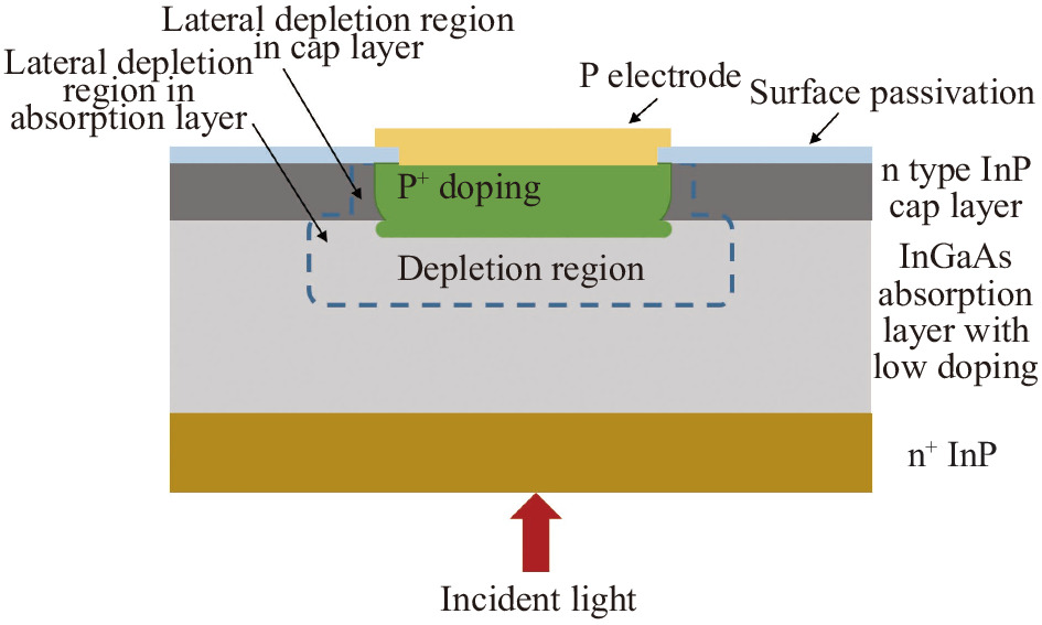
图 1 平面型In0.53Ga0.47As探测器剖面结构
Figure 1. Profile structure of planar In0.53Ga0.47As detector
$$ {C_j} = {{A}}\dfrac{{{\varepsilon _0}{\varepsilon _s}}}{{{W_d}}} $$ (1) 式中:A为探测器的结面积;ε0为真空介电常数;εs为半导体的介电常数;Wd为耗尽区的宽度,耗尽区的宽度越宽,单位面积的结电容越小。耗尽层宽度Wd和外加电压V以及吸收层掺杂浓度Nd之间的关系为:
$$ {W_d} = {\left[ {\dfrac{{2{\varepsilon _0}{\varepsilon _s}}}{q}\dfrac{{{V_0} - V}}{{{N_d}}}} \right]^{1/2}} $$ (2) 式中:V0为P+n结的内建电势,将公式(2)代入公式(1),并重新整理可得:
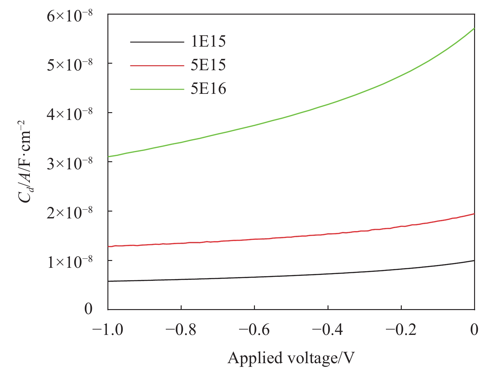
$$ \frac{1}{{C_j^2}} = \dfrac{2}{{q{\varepsilon _0}{\varepsilon _s}{N_d}}}\left( {{V_0} - V} \right) $$ (3) 因此,降低材料吸收层的掺杂浓度可以有效减小探测器的结电容。采用不同吸收层浓度的材料制备的探测器的单位面积电容与电压的关系如图2所示,可见降低吸收层掺杂浓度,可有效抑制探测器电容。

图 2 不同吸收层浓度的探测器的C-V特性
Figure 2. C-V curve of detectors with different doping absorption layers
图3为采用相同材料和工艺制备的不同直径的光敏元的暗电流密度,在室温−0.1 V偏压下,500 μm直径的单元器件暗电流密度为3.34 nA/cm2,而10 μm直径的单元器件暗电流密度为53.53 nA/cm2,暗电流密度增大了16倍之多。这说明针对高密度小像元探测器的暗电流,需要进行优化。
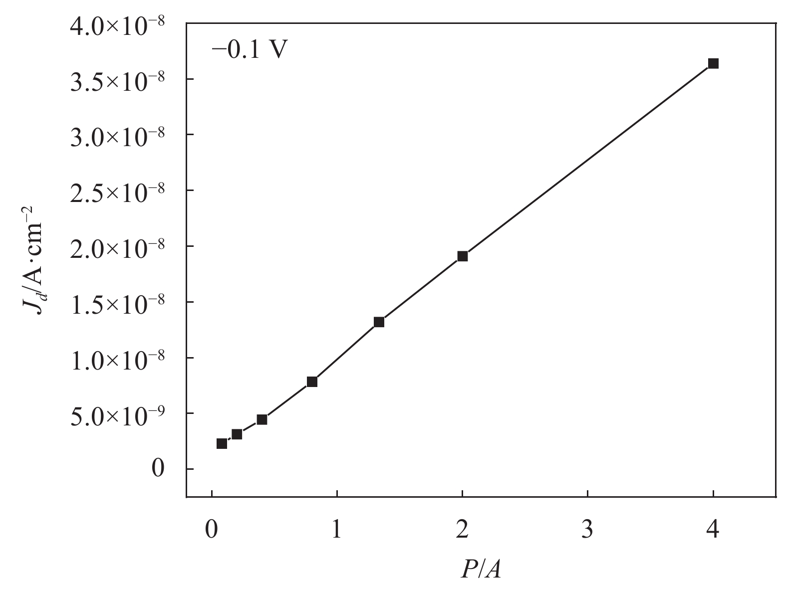
光敏芯片的暗电流由体电流和表面及侧面电流组成,体电流与光敏芯片的面积A成正比,而表面及侧面电流与光敏元的周长P成正比。探测器的光敏元暗电流密度可以表示为:
$$ J = \dfrac{I}{A} = {J_B} + {J_S}\dfrac{P}{A} $$ (4) 式中:JB为体内漏电流密度;JS为表面和侧面漏电流密度。计算不同尺寸的探测器暗电流密度和P/A的关系,可以分析出在总暗电流中体电流和表面及侧面漏电的贡献。从图4可以看出,随着P/A的增大,暗电流密度呈直线增大,表明与周长相关的侧面漏电和表面漏电作用凸显,需要优化器件表面钝化工艺,降低表面漏电。

图 3 不同尺寸的InGaAs探测器的暗电流密度
Figure 3. Dark current density of InGaAs detectors with different sizes

图 4 暗电流密度与P/A的关系
Figure 4. Relationship between dark current density and P/A
采用低温ICPCVD方式镀SiNx钝化膜,调整镀膜过程中的气体总流量、N2/SiH4比例以及腔体压强,保持生长腔体温度和ICP功率不变,优化高密度小像元器件表面的钝化工艺,抑制表面漏电,最终有效降低了高密度小像元阵列探测器的暗电流。室温下−0.1 V偏压,15 μm中心距器件暗电流密度为9.43 nA/cm2,12 μm中心距器件暗电流密度为11.02 nA/cm2,10 μm中心距器件暗电流密度为11.62 nA/cm2,如图5所示。
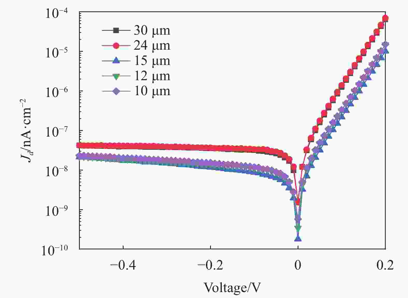
图 5 室温不同中心距器件暗电流密度
Figure 5. Dark current density of different pitch array devices at room temperature
-
InGaAs焦平面探测器采用光敏芯片和读出电路混成互连构成焦平面器件,互连方式有直接倒焊混成、间接倒焊混成、环孔技术和引线键合等。直接倒焊混成型红外焦平面是当前发展最为成熟的焦平面结构,其优点是敏感元阵列可获得接近100%的占空因子、读出电路可增大信号处理器的面积、互连寄生参数小、传输速率快、抗电磁干扰能力强和机械可靠性高等。随着焦平面规模从320×256、640×512、1280×1024扩大到2560×2048,像元中心距由30 μm、15 μm缩小到10 μm,焊点密度不断提高,对混成互连提出了较高的要求。通过对芯片表面状态、倒焊参数、倒焊偏移控制等影响倒焊连通率的全因素分析,结合已有规格面阵倒焊技术,明确了制约500万像素级大面阵倒焊连通率的主要因素,一方面是光敏芯片和读出电路样品的状态,包括芯片样品的平面度(面形)、互连凸点的材质与状态、样品表面和背面的洁净度和图形对齐情况等;另一方面是倒焊互连过程,包括倒焊前预处理、倒焊方式和倒焊温度、压力等参数。
(1)高平整度芯片减薄抛光与面型调控技术
芯片翘曲是影响倒焊连通率的关键因素之一,当芯片翘曲超出铟柱凸点的有效接触范围,倒焊互连时部分的铟柱将无法形成良好的电学连通,从而形成死像元,导致连通率降低;且随着面阵规模扩大,芯片的平面度问题愈加凸显,需要更加严格控制芯片平面度以满足高密度倒焊互连的要求。针对芯片的平面度问题,首先对材料进行初始面型筛选,挑选平面度优于20 μm的材料进入流片,流片过程中监测平面度变化;衬底减薄抛光采用化学机械抛光(CMP)工艺进行,通过优化减薄抛光过程中研磨液的粒径、公转速、自转速、压力等可以实现晶圆较好的平整度。
另一方面在研制过程中采用应力平衡膜工艺进行芯片面形调控,即在InGaAs/InP探测器晶圆的背面,生长具有低应力的SiNx或SiO2介质膜。通过对介质膜生长工艺的调控,改变整个晶圆的宏观形变,使得原本中心翘曲的晶圆恢复至平面状态。如图6所示,随着平衡膜厚度的增加,晶圆逐渐恢复至接近平面的状态,满足倒焊连通对光敏芯片平面度的要求。

图 6 随平衡膜厚度增加芯片平面度的变化
Figure 6. Change of chip flatness with the increase of balance film thickness
(2)凸点形貌和一致性控制
红外探测器通常采用金属铟作为互连凸点材料,如图7所示,高低不一的铟柱阵列会导致倒焊互连后死像元的出现;而铟柱形貌不均匀,则有可能造成两元横向互连短路,形成过热像元。

图 7 铟柱凸点形貌和一致性对连通率的影响
Figure 7. Influence of the morphology and consistency of the indium pillar bumps on the connectivity rate
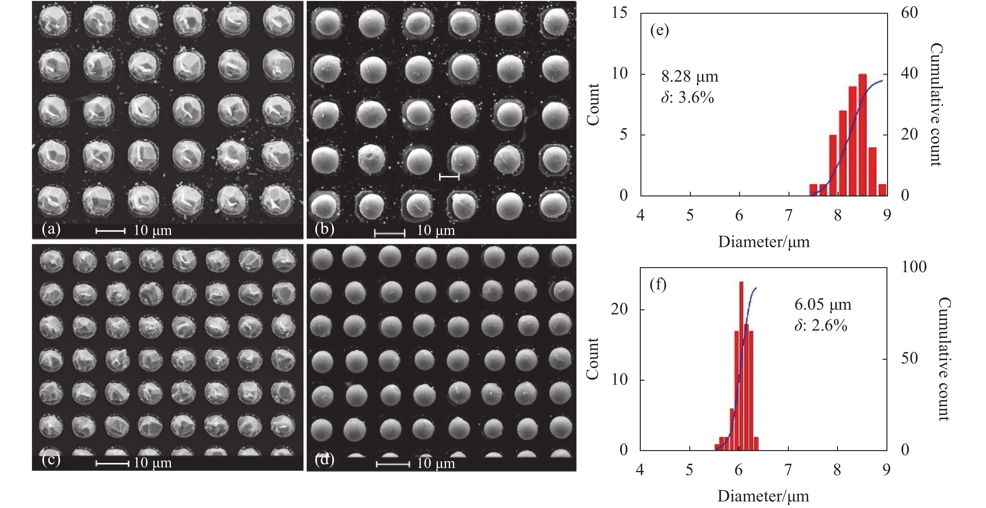
为提高焦平面探测器的连通率,需尽可能提升铟柱的高度、形状饱满度和一致性。影响铟柱形貌的因素有,铟柱制备工艺流程、光刻参数、铟柱蒸发工艺参数等。图8(a)为焦平面探测器铟柱制备的常规流程,先制备Cr/Ni/Au结构的多层金属膜UBM(Under Bump Metallurgy),其中Cr层充当阻挡层和粘合层,而Ni层在回流过程中可被铟浸润,而Au是保护层,有助于在回流过程中固定铟柱位置,然后进行正胶光刻、蒸发和剥离。对于中心距大于15 μm的探测器,通过这种工艺流程即可实现均匀的铟柱阵列。然而当中心距低至10 μm时,均匀性问题变得越来越明显。而且此时整个芯片面积上的铟柱阵列的填充因子已经超过50%,因此铟柱的剥离变得特别困难,因此容易出现铟柱的缺失或残留。为了抑制上述缺陷,对铟柱生长工艺流程进行了优化。如图8(b)所示,在铟柱光刻之前,引入钝化膜塑形工艺,对铟柱的形貌进行调控。光刻工艺采用负胶光刻,形成易剥离的底切结构。在铟柱生长完成后,再对铟柱进行回流成球,获得形貌一致性好的铟球阵列[10]。

图 8 铟柱生长工艺流程。 (a) 原流程 ;(b) 改进流程
Figure 8. Indium bump growth process. (a) Original process; (b) Improved process
采用图8(b)中所示的改进工艺流程制备出了满足高密度焦平面高连通率倒焊要求的铟柱阵列,如图9所示。像元中心距15 μm的铟柱直径统计平均为8.28 μm,变异系数为3.6%,像元中心距10 μm的铟柱直径统计平均为6.05 μm,变异系数为3.6% ,2.6%,铟柱的尺寸饱满、均匀性高。

图 9 采用优化工艺制备的铟柱回融前后的形貌 。(a) 15 μm中心距铟柱回融前SEM图; (b) 15 μm中心距铟柱回融后SEM图;(c) 10 μm中心距铟柱回融前 SEM图;(d) 10 μm中心距铟柱回融后SEM图; (e) 15 μm中心距铟柱直径统计分布 ;(f) 10 μm中心距铟柱直径统计分布
Figure 9. Indium bump arrays fabricated via the modified SiNx recipe: SEM images for 15 μm pitch (a) before and (b) after reflow, and 10 μm pitch (c) before and (d) after reflow; (e) and (f) Statistical diameter distribution of the ball arrays for 15 μm pitch and 10 μm pitch respectively
(3)高密度倒焊工艺优化
均匀一致性的模块耦合互连是实现高均匀性焦平面组件的关键之一。光敏芯片和读出电路芯片耦合过程中存在接触电阻。这些电阻是随机的,分析表明,在运放积分模式中,存在接触电阻时,光敏元工作点将偏离零偏,电流发生变化,从而对器件的响应均匀性产生显著的影响;这些接触电阻的起因是由于金属化表面或In柱表面存在或多或少的氧化层所致,实验表明:在金属化或生长In柱时,采用离子束清洗技术可以有效地降低接触电阻。随着焦平面规模扩大到2560×2048,像元中心距缩小到10 μm,焊点密度大大提高,倒焊偏移量容差已接近倒焊精度极限,对倒焊互连工艺提出了巨大的挑战。此外,倒焊耦合互连参数会影响器件的性能,如倒焊压力过大,会损坏器件或将相邻铟柱压扁连在一起,造成死像元或过热像元,引起器件响应均匀性下降,因此,在器件结构和电路结构设计的基础上,优化倒焊耦合参数,实现均匀一致的倒焊耦合互连技术。
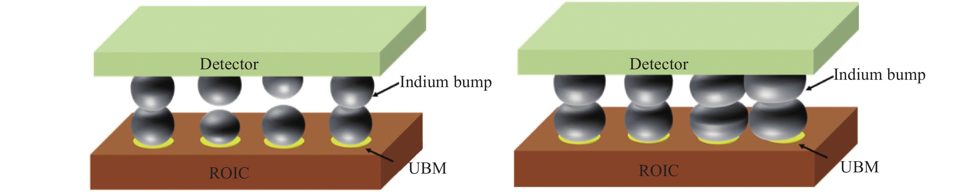
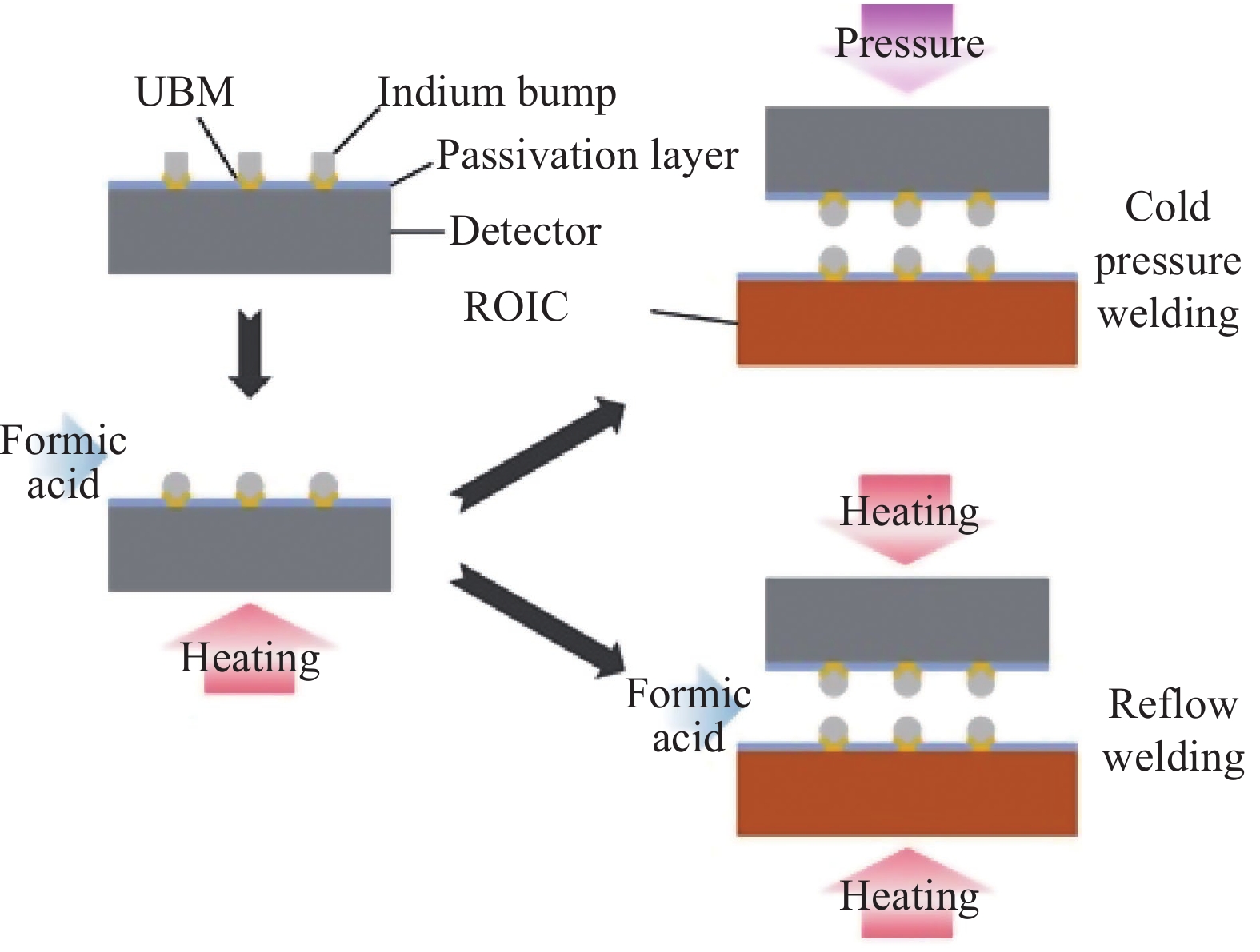
常用的倒焊工艺方法有冷压焊和回熔焊,如图10所示。冷压焊是在光敏芯片和读出电路各元对准的基础上,通过施加一定的压力,使得光敏芯片和读出电路结合在一起,冷压焊过程容易产生随机的水平偏移。热压焊是在倒焊的过程中提高光敏芯片和读出电路的温度,再通过施加压力的方式使二者互连的工艺,高温对准互连后的焦平面需要考虑材料之间热膨胀不匹配的问题。回熔焊是将光敏芯片和读出电路置于高温和还原性气氛(如甲酸)中,去除铟柱表面氧化层引起焊料回流并形成光敏芯片和读出电路之间的物理连接,回熔焊工艺中不需要施加压力,倒焊后水平偏移较小。
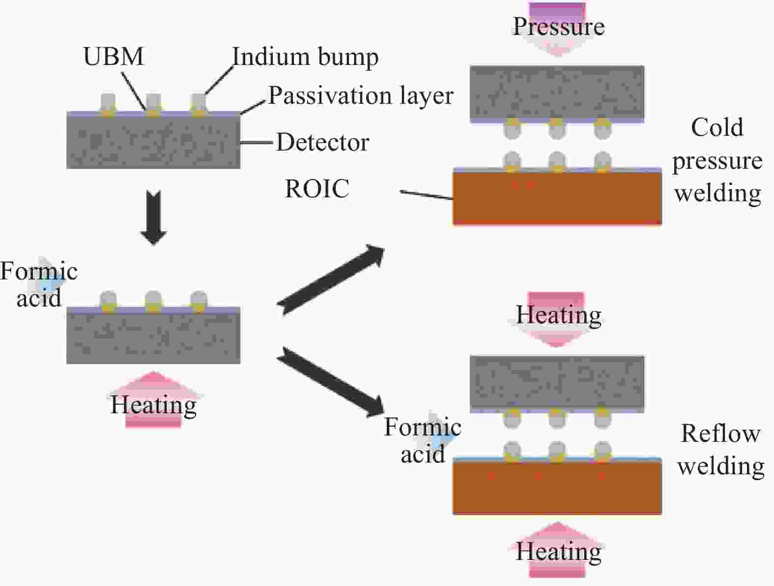
图 10 焦平面的倒焊互连
Figure 10. Hybridization of focal plane
通过对比冷压焊和回熔焊的工艺特点不难发现,单纯依靠某一种方式实现高连通率的大规模高密度焦平面互连耦合将非常困难。开展2560×2048(10 μm间距)焦平面倒焊工艺的探索与优化,先通过回熔焊工艺使光敏芯片和读出电路初步形成互连,再采用高平整度材料作为倒焊过渡结构,通过倒焊过渡结构与初步互连的焦平面模块二次冷压焊使光敏芯片和读出电路实现完全互连。将回熔焊和冷压焊工艺有机融合,充分发挥两种工艺的优点,在减小倒焊随机偏移的同时克服了由芯片平整度和铟柱质量引起的互连不上的问题,从而有效提高大规模高密度焦平面探测器的连通率和倒焊成品率。采用新工艺倒焊的10 μm中心距2560×2048元InGaAs焦平面,盲元率低至0.26%。
-
对研制的10 μm中心距2560×2048元InGaAs焦平面探测器组件进行光电性能测试,测试条件如表1所示(表中,1 in=2.54 cm)。
表 1 2560×2048元InGaAs焦平面探测器测试条件
Table 1. Test conditions of 2560×2048 InGaAs focal plane arrays
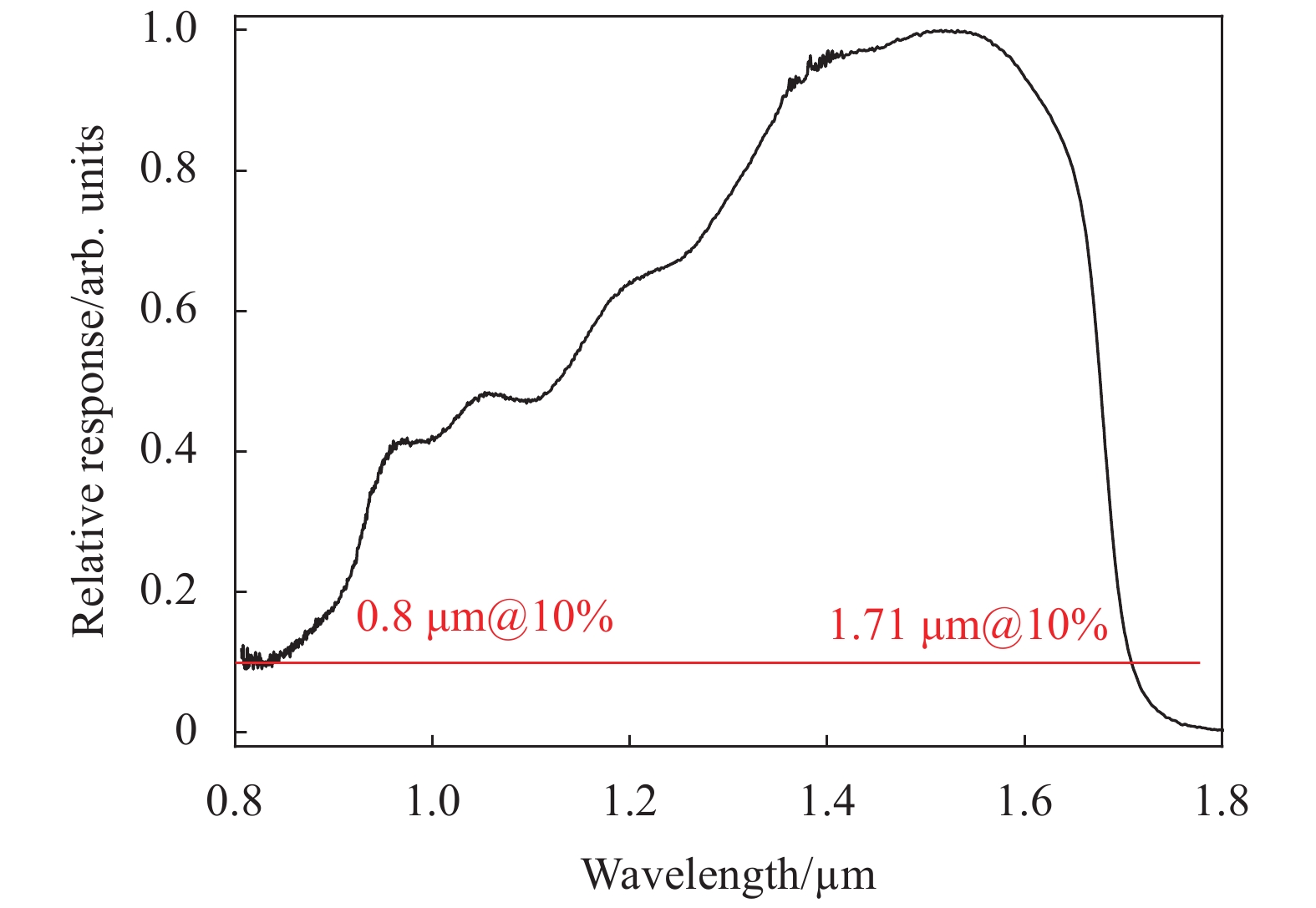
Item Value Item Value Black body temperature/K 900 Black body aperture/in 0.1 Distance/cm 60 Blackbody radiated power/W 1.65×10⁻¹¹ Ambient temperature/℃ 22 Ambient humidity 23% Operating temperature/K 276 Circuit gain 0.8 Integral time/ms 100 Integral capacitance/fF 15 如图11所示为焦平面的响应光谱曲线,从图中可以看出,2560×2048元InGaAs焦平面光谱响应范围为0.80~1.71 µm。
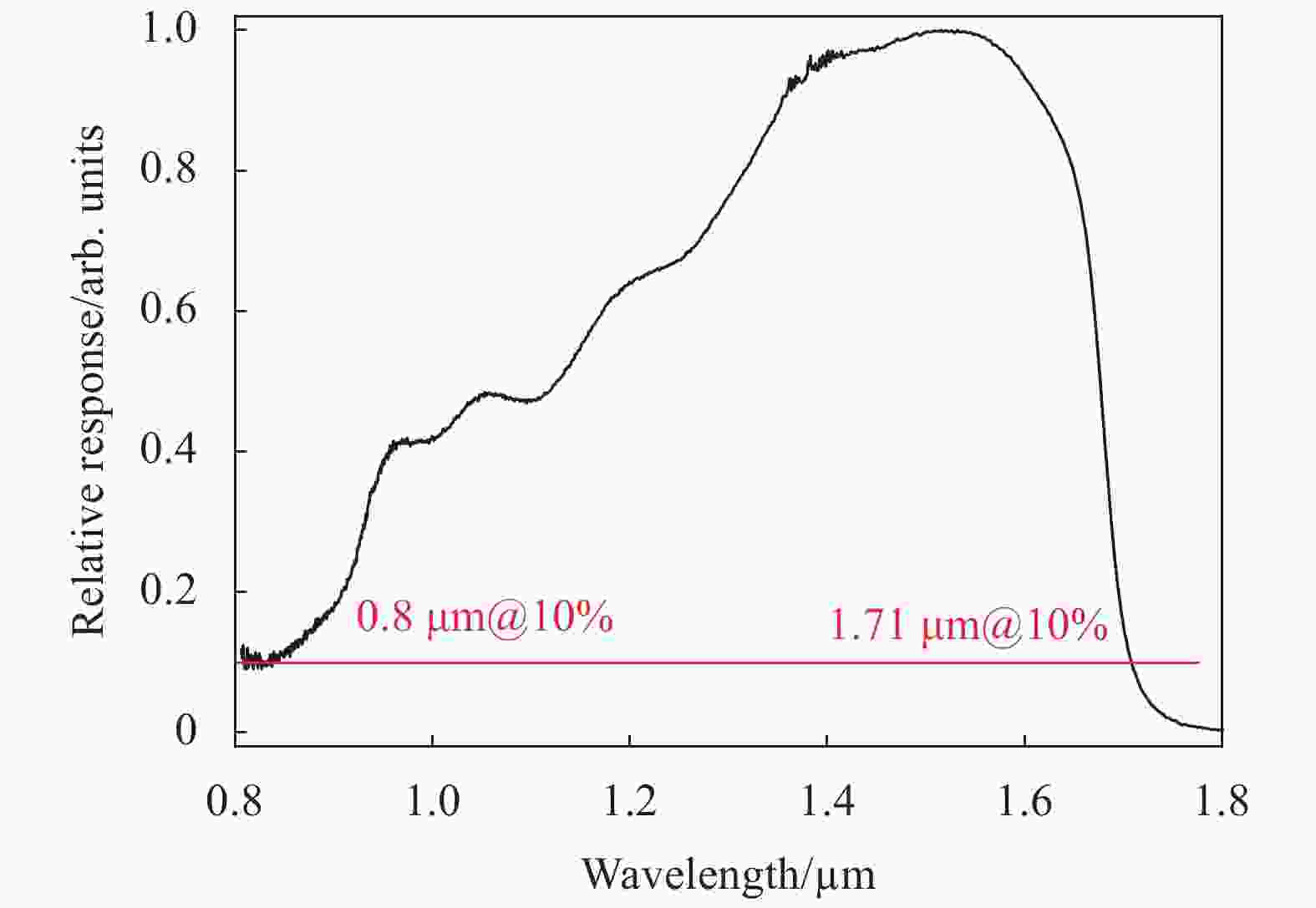
图 11 2560×2048元InGaAs焦平面探测器组件光谱响应曲线
Figure 11. Response spectra curve of 2560×2048 InGaAs focal plane arrays
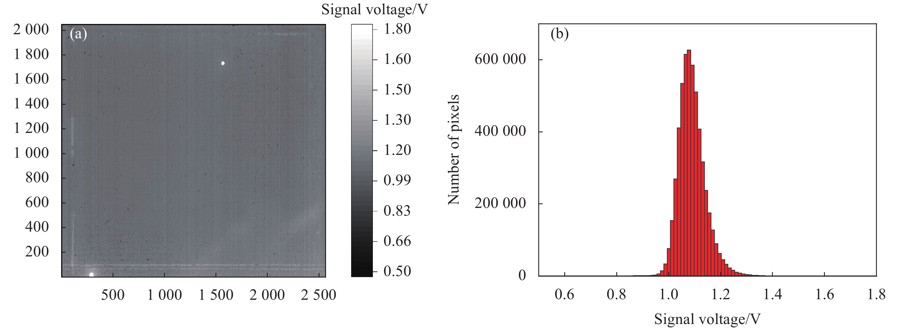
焦平面黑体响应信号如图12所示,测得黑体响应信号Vs=1.071 V,响应非均匀性为3.81%,盲元率0.26%。
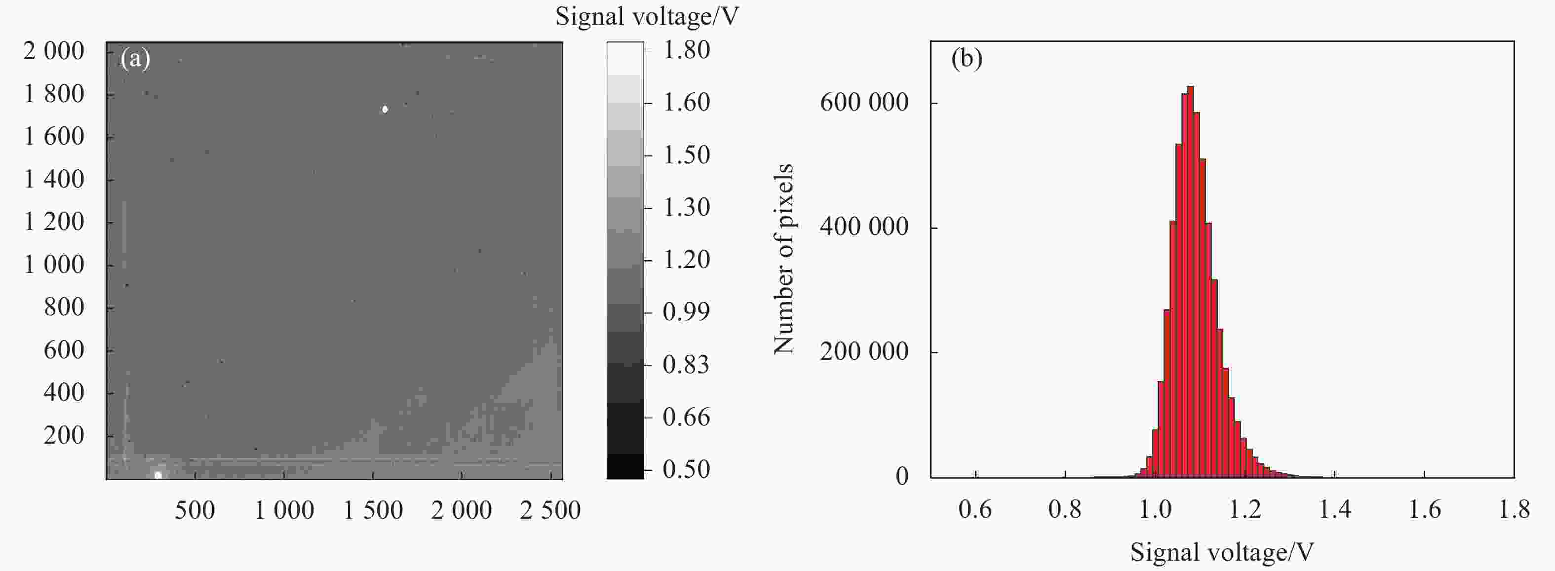
图 12 焦平面响应信号测试结果。(a) 像元信号图;(b) 信号统计分布
Figure 12. Measured result of response signal of FPAs. (a) Pixel signal map; (b) Signal statistical distribution
焦平面噪声测试结果如图13所示,噪声电压为1.02 mV。

图 13 焦平面噪声测试结果。(a) 像元噪声图;(b) 噪声统计分布
Figure 13. Measured result of noise of FPAs. (a) Pixel noise map; (b) Noise statistical distribution
焦平面的响应率R、探测率D*和量子效率η分别为:
$$ {{{R}}_i} = \dfrac{{{V_s}{C_{int}}}}{{{T_{int}}{A_v}P}}G $$ (5) $$ {{{D}}^*} = G\sqrt {\dfrac{{{A_D}}}{{2{T_{int}}}}} \cdot \dfrac{{{V_S}}}{{P{V_N}}} $$ (6) $$ \eta = hc\dfrac{{{R_i}}}{{q{\lambda _p}}} $$ (7) 式中:Vs为平均信号值;VN为平均噪声值;Cint为积分电容;Tint为积分时间;Av为电路增益,取值0.8;G因子为光谱因子,值取78;h为普朗克常数;c为真空光速;
${\lambda _p} $ 为峰值波长,为1.6 μm。根据测得的光谱响应、信号、噪声,计算得到焦平面的响应率为0.95 A/W,量子效率为73.7%,峰值探测率为1.11×1013 cm·Hz1/2/W。采用了高动态范围(High-Dynamic Range, HDR)技术进行试验,通过两次或多次采样(Multiple Capture),当目标物的光强时,采用短积分时间Tint1;当目标物的光弱时,采用长积分时间Tint2,综合得到整个目标内的光强分布,获得大动态范围。采用短波红外激光器(MIL-1342 nm,200 mW)照到墙壁上,形成圆斑区域强光,读出电路饱和信号Vsat约为1.85 V。采用HDR技术,读出电路试验片Tint1=0.06 ms、Tint2=100 ms,成像图像如图14所示:等效的饱和信号约为2.604 V,动态范围增大到128.1 dB。
图 14 采用HDR技术的成像验证
Figure 14. Imaging verification using HDR technology
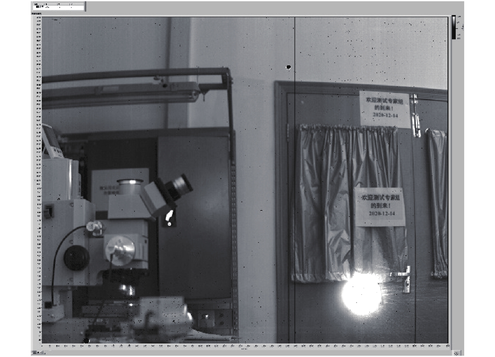
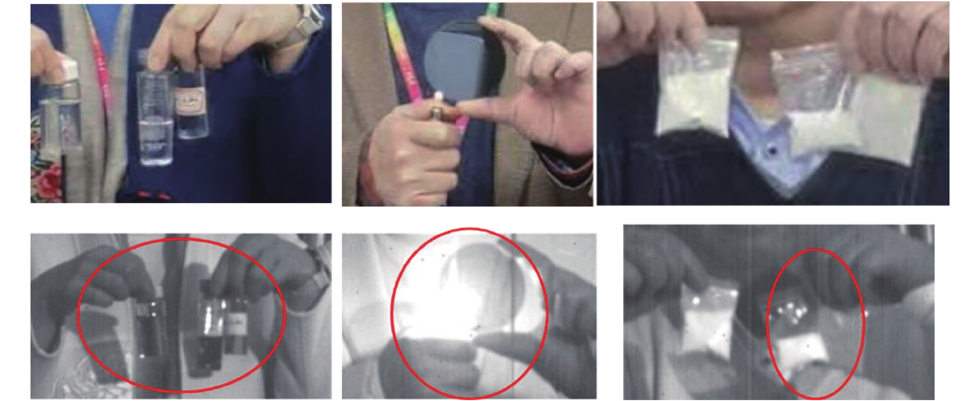
如图15所示,采用2560×2048元InGaAs焦平面探测器组件进行成像验证。如图16所示,短波红外成像可以清晰地辨别液位、穿透硅片对背后的火焰成像,以及具有分辨不同物质的能力。
图 15 10 μm中心距2 560×2 048元InGaAs焦平面组件成像验证
Figure 15. Imaging verification of 10 μm pitch 2560×2048 InGaAs focal plane arrays
图 16 可见与短波红外成像的细节对比
Figure 16. Comparison of the details of visible and short-wave infrared imaging
-
中国科学院上海技术物理研究所通过高密度小光敏元探测器暗电流与噪声抑制、大规模焦平面集成等技术的突破,研制出国内首个10 μm中心距2560×2048元InGaAs焦平面组件(图17),工作波长覆盖0.9~1.7 µm,室温下暗电流密度为11.62 nA/cm2,焦平面有效像元率高达99.7%,峰值探测率1.11×1013 cm·Hz1/2/W,HDR模式下动态范围可达128.1 dB,并获得了清晰的实验室成像照片。

图 17 2560×2048 InGaAs-10 μm焦平面。 (a) 光敏芯片; (b) 读出电路; (c) 焦平面
Figure 17. 10 μm pitch 2560×2048 InGaAs focal plane arrays. (a) Photosensitive chip; (b) Readout circuit; (c) Focal plane
2560×2048 short-wave infrared InGaAs focal plane detector (Invited)
-
摘要: 高性能大规模小像元短波红外InGaAs焦平面探测器是新一代航天遥感仪器向高空间分辨率、高能量分辨率、高时间分辨率发展需要的核心器件。文中报道了高密度InGaAs探测器阵列设计与制备,并与匹配的Si-CMOS读出电路倒焊互连形成焦平面的最新研究进展,重点突破了高密度小像素探测器的暗电流和噪声抑制、百万像素焦平面倒焊互连等关键技术,解决了高平整度芯片面形控制、In柱凸点形貌和高度一致性控制、高密度倒焊偏移控制等倒焊新工艺,研制了像元中心距10 μm的2560×2048元焦平面探测器,其峰值探测率优于1.0×1013 cm·Hz1/2/W,响应不均匀性优于3%,有效像元率优于99.7%,动态范围优于120 dB。采用该焦平面进行了实验室演示成像,图片清晰。Abstract: The new generation of aerospace remote sensing instruments are developing towards high spatial resolution, high energy resolution, and high time resolution. Its core components are high-performance large-scale small-pixel short-wave infrared InGaAs focal plane detectors. The latest research progress in the design and fabrication of high-density InGaAs detector arrays was reported, and hybrided with matching Si-CMOS readout circuits to form a focal plane. The breakthroughs in dark current and noise suppression of high-density small-pixel detectors , megapixel focal plane flip chip interconnection and other key technologies were focused. The new flip chip interconnection technologies such as high flatness chip surface shape control, indium bumps convex morphology and high consistency control, and high-density flip chip interconnection control were solved. Developed 10 μm pitch 2560×2 048 focal plane detectors, which D* was better than 1.0×1013 cm·Hz1/2/W, the response non-uniformity was better than 3%, the effective pixel rate was better than 99.7%, and the dynamic range was better than 120 dB. This focal plane was used for laboratory demonstration imaging, and the picture was clear.
-
Key words:
- InGaAs /
- focal plane /
- short-wave infrared /
- detectivity /
- dark current
-
图 1 平面型In0.53Ga0.47As探测器剖面结构
Figure 1. Profile structure of planar In0.53Ga0.47As detector
图 2 不同吸收层浓度的探测器的C-V特性
Figure 2. C-V curve of detectors with different doping absorption layers
图 3 不同尺寸的InGaAs探测器的暗电流密度
Figure 3. Dark current density of InGaAs detectors with different sizes
图 5 室温不同中心距器件暗电流密度
Figure 5. Dark current density of different pitch array devices at room temperature
图 6 随平衡膜厚度增加芯片平面度的变化
Figure 6. Change of chip flatness with the increase of balance film thickness
图 7 铟柱凸点形貌和一致性对连通率的影响
Figure 7. Influence of the morphology and consistency of the indium pillar bumps on the connectivity rate
图 8 铟柱生长工艺流程。 (a) 原流程 ;(b) 改进流程
Figure 8. Indium bump growth process. (a) Original process; (b) Improved process
图 9 采用优化工艺制备的铟柱回融前后的形貌 。(a) 15 μm中心距铟柱回融前SEM图; (b) 15 μm中心距铟柱回融后SEM图;(c) 10 μm中心距铟柱回融前 SEM图;(d) 10 μm中心距铟柱回融后SEM图; (e) 15 μm中心距铟柱直径统计分布 ;(f) 10 μm中心距铟柱直径统计分布
Figure 9. Indium bump arrays fabricated via the modified SiNx recipe: SEM images for 15 μm pitch (a) before and (b) after reflow, and 10 μm pitch (c) before and (d) after reflow; (e) and (f) Statistical diameter distribution of the ball arrays for 15 μm pitch and 10 μm pitch respectively
图 11 2560×2048元InGaAs焦平面探测器组件光谱响应曲线
Figure 11. Response spectra curve of 2560×2048 InGaAs focal plane arrays
图 12 焦平面响应信号测试结果。(a) 像元信号图;(b) 信号统计分布
Figure 12. Measured result of response signal of FPAs. (a) Pixel signal map; (b) Signal statistical distribution
图 13 焦平面噪声测试结果。(a) 像元噪声图;(b) 噪声统计分布
Figure 13. Measured result of noise of FPAs. (a) Pixel noise map; (b) Noise statistical distribution
图 15 10 μm中心距2 560×2 048元InGaAs焦平面组件成像验证
Figure 15. Imaging verification of 10 μm pitch 2560×2048 InGaAs focal plane arrays
图 16 可见与短波红外成像的细节对比
Figure 16. Comparison of the details of visible and short-wave infrared imaging
图 17 2560×2048 InGaAs-10 μm焦平面。 (a) 光敏芯片; (b) 读出电路; (c) 焦平面
Figure 17. 10 μm pitch 2560×2048 InGaAs focal plane arrays. (a) Photosensitive chip; (b) Readout circuit; (c) Focal plane
表 1 2560×2048元InGaAs焦平面探测器测试条件
Table 1. Test conditions of 2560×2048 InGaAs focal plane arrays
Item Value Item Value Black body temperature/K 900 Black body aperture/in 0.1 Distance/cm 60 Blackbody radiated power/W 1.65×10⁻¹¹ Ambient temperature/℃ 22 Ambient humidity 23% Operating temperature/K 276 Circuit gain 0.8 Integral time/ms 100 Integral capacitance/fF 15  下载: 导出CSV
-
[1] Judd K P, Nichols J M, Howard J G, et al. Passive shortwave infrared broadband and hyperspectral imaging in a maritime environment [J]. Optical Engineering, 2012, 51(1): 3202. [2] Macdougal M, Hood A, Geske J, et al. InGaAs focal plane arrays for low-light-level SWIR imaging[C]//Proceedings of SPIE, 2011, 8012: 801221. [3] Battaglia J, Blessinger M, Enriquez M, et al. An uncooled 1280×1024 InGaAs focal plane array for small platform, shortwave infrared imaging[C]//Proceedings of SPIE, 2009, 7298: 72983 C. [4] Yuan H, Andresen B F, Fulop G F, et al. FPA development: From InGaAs, InSb, to HgCdTe[C]//Proceedings of SPIE, 2008, 6940: 69403 C. [5] John Liobe, Michael Daugherty, Paul Bereznycky, et al. Ultra-large format, ultra-small pixel pitch extended response visible through short-wave infrared (SWIR) camera[C]//Proceedings of SPIE, 2019, 11002, [6] Manda S, Matsumoto R, Saito S, et al. High-definition visible-SWIR InGaAs image sensor using Cu-Cu bonding of III-V to silicon wafer[C]//2019 IEEE International Electron Devices Meeting (IEDM). IEEE, 2019. [7] Macdougal M H, Hood A, Geske J, et al. Small pixel VGA SWIR cameras for laser sensing (Conference Presentation)[C]//Proceedings of SPIE, 2020, 11407: 1140703. [8] Li Xue, Shao Xiumei, Li Tao, et al. Developments of short-wave infrared InGaAs focal plane detectors [J]. Infrared and Laser Engineering, 2020, 49(1): 0103006. (in Chinese) doi: 10.3788/IRLA202049.0103006 [9] Shao Xiumei, Gong Haimei, Li Xue, et al. Developments of high performance short-wave infrared InGaAs focal plane detectors [J]. Infrared Technology, 2016, 38(8): 629-635. (in Chinese) [10] Ma Yingjie, Zhu Xianliang, Yang Bo, et al. Fabrication of highly-uniform indium ball bumps for small unit-cell infrared focal plane arrays[C]//Conference on Infrared Device and Infrared Technology, 2020. -

 点击查看大图

计量
- 文章访问数: 810
- HTML全文浏览量: 141
- PDF下载量: 248
- 被引次数: 0


