


 下载:
下载:


-
自1917年首个红外探测器问世以来,其在军用与民用等诸多领域的需求与日俱增,例如导弹追踪、侦查夜视、安防监控、搜索救援、医疗诊断、材料检测以及测温防疫等等[1]。近年来,红外探测的需求不断增加。目前,市面上成熟的红外探测技术主要是以基于Si、Ge、InAs、InGaAs、HgCdTe等材料的平面半导体探测器为主[2-4],然而由于室温电子能量(0.026 eV)与红外尤其是中远红外光能量相当,随着入射光波长的增加,光电流与室温环境难以分辨,探测率会急剧下降。常用的高精度探测器包括HgCdTe[2]、InAs/InGaSb Ⅱ类超晶格[3]、GaAs/AlGaAs量子阱[4]等都为制冷型探测器,然而该型探测器功耗较高,体积庞大,价格昂贵等缺点严重限制了其在多领域的应用。此时,室温宽谱段、超高灵敏度、超快响应、超小像元、轻型化、低成本的红外探测需求被提出,新型低维半导体光电探测器的发展迎来了机遇和挑战[5-6]。
随着摩尔定律接近极限,传统硅基半导体制造的经典物理理论不再适用,短沟道效应等问题严重影响其性能,此时,低维半导体材料的应用将有望实现集成电路工艺新突破,以及在硅衬底上外延生长III-V族等高迁移率材料形成的新型高性能低功耗器件将有可能成为下一代逻辑器件的基础[7]。因此,对于低维纳米材料的研究成为半导体行业最具前沿性的工作之一。其中,纳米线相较于传统体材料来说,由于其尺寸与维度的减小,展现了高比表面积、量子效应、表面与界面效应等独特的物理特性,加之其制备技术与硅工艺兼容,有望通过实现全环绕栅极晶体管结构来替代鳍式晶体管结构,进一步缩小晶体管尺寸,提高性能,降低能耗[8]。基于以上,当纳米线被应用于红外光电探测时,展现了巨大的优势与潜力,例如降低暗电流、提高光吸收效率、延长光载流子寿命、分离与收集光电子、减小探测器件尺寸与能耗等等[9-11]。
为了实现半导体纳米线的高性能红外探测应用,可控生长均一、高质量的半导体纳米线是关键。当前,许多材料纳米线通过“自上而下”或“自下而上”的方法已被合成并应用于红外光电探测[11],比如IV族的Si[12]、Ge[13]纳米线,III-V族的GaAs[14]、GaSb[15-18]、InSb[19]、InP[20]、InAs[21-23]纳米线,II-V族的SnSe[24]、SnS[24]纳米线等,并且多种方法也被用于进一步提高纳米线的光电性能[25-26],这些都展示了纳米线在未来红外探测器发展中的巨大优势与潜力。
文中主要从半导体纳米线制备出发介绍了纳米线红外探测器,并从沟道材料的选择与生长、异质结合、外场调控以及探测器件的功能集成等方面分类总结了近年来纳米线红外探测器的研究进展。
-
纳米线被定义为直径在100 nm以下的一维结构,与传统的体材料相比,纳米线的电子仅能在一个维度方向移动,被认为是电子输运的理想材料[8]。此外,纳米线在光电探测应用上也有着独特的优势,例如,减小的尺寸与维度可利于降低暗电流,缩小器件尺寸,减少器件能耗[27];超高的比表面积与德拜长度可有效提高光吸收效率,延长光载流子寿命,缩短载流子传输时间[10];丰富的表面态可被用于调控光电性能例如促进光电子的分离与收集等[9, 21];纳米线侧壁应力释放的增强以及与衬底较小的接触面积,能够大幅度降低晶格失配在外延生长中的阻碍作用[28];纳米线制备工艺与传统硅基工艺的兼容性,可促进其在集成电路中的广泛应用[29]。
-
由于光电导效应产生条件,半导体禁带宽度决定了红外探测器的探测范围,图1展示了大部分被用于红外探测的经典半导体材料[30],其低温禁带宽度均低于2.5 eV,交替覆盖了从近红外到中红外的波长范围。其中,Ⅲ-Ⅴ族半导体纳米线由于迁移率高、俄歇寿命长、吸收系数高、覆盖波长范围广等优势,已被广泛的用于红外探测研究[5, 31-32]。连接线代表不同材料结合可调带隙范围。
-
纳米线的制备方法通常可以分为两种:“自上而下”和“自下而上”:
(1) “自上而下”主要是通过刻蚀或纳米刻印技术将块体材料缩小到纳米尺寸,这种方法可以保留原体材料的物理特性,如晶体生长方向,杂质浓度等,然而产量低,损耗大,成本高,其方法主要有反应离子刻蚀,金属辅助化学刻蚀等[33]。
(2) “自下而上”主要采用气相生长[15]、液相生长[19]、模板辅助生长[33]等方式,将原子、分子或纳米粒子等小结构单元通过相互作用自组装成相对较大,较复杂的纳米结构体系。这种方法节省材料,并且可通过生长条件的改变对纳米线的形貌、成分、尺寸、掺杂等特性进行精确调控[20]。文中所涉及制作红外探测器的半导体纳米线主要为气相生长,包括物理气相沉积(PVD)、化学气相沉积(CVD)、激光辅助化学气相沉积(LACVD)、金属有机物化学气相沉积(MOCVD)以及分子束外延(MBE)等。接下来,主要通过CVD方法介绍气相沉积生长机理。
在过去十几年中,CVD方法由于生长速率快,重复性高,成本低廉,易于操作等优势已被广泛地用于半导体纳米线的生长中。该方法生长过程如图2(a)所示:首先,源材料被放置于管式炉上游区,在高温加热后形成气体前驱物,并经载气传输至下游生长区;生长区衬底上预先沉积有金属薄膜,经高温退火后融化成金属颗粒,然后吸收载气中的源气体前驱物形成催化合金,当催化合金达到饱和状态时,前驱体原子沿特定晶向的催化合金界面析出,生成纳米线[15]。

图 2 (a) CVD装置示意图[15];(b) 纳米线VLS和VSS生长机理示意图[34];(c) 传统纳米线生长与表面活性剂辅助纳米线生长机理示意图[17]
Figure 2. (a) Schematic representation of the CVD setup[15]; (b) Schematic illustration of the VLS and VSS growth mechanism[34]; (c) Schematic illustration of the conventional and the surfactant-assisted nanowire (NW) growth mode[17]
传统的CVD生长通常有两种机理:气液固(VLS)生长与气固固(VSS)生长机理,如图2(b)所示,当纳米线生长温度高于催化合金共晶温度时,催化剂尖端呈液态,为VLS生长,反之催化剂尖端呈固态,为VSS生长[34]。利用两种生长模式,Yang等在2017年实现了纳米线生长方向可控。这是因为,在VLS生长过程中,部分液态催化剂移动聚集成大液滴,导致催化剂颗粒大小不同,由于吉布斯-汤姆逊效应,催化剂颗粒大小会影响催化剂合金过饱和时合金的比例,即影响最低能量界面,进而导致纳米线的直径与生长方向不均一;而在VSS生长中,不可移动的固态催化剂,沿最低表面能的密排面生长,形成不同长度相同直径的圆柱形,并且纳米线生长方向由催化剂与纳米线界面决定,因此相较于VLS生长机理,VSS所生长的纳米线有更均一的直径与生长方向。基于此原理,Yang等通过使用CMOS兼容的Pd金属催化CVD方法实现了GaSb纳米线的VSS生长,得到了均匀直径、高迁移率、均一生长方向的GaSb纳米线[16]。
除此之外,早在2014年,Yang等就已经通过引入表面活性剂钝化纳米线表面来实现纳米线直径可控,如图2(c)所示。这是由于在纳米线的生长过程中,除了VLS生长模式,还有气-固(VS)生长模式,即前驱体原子不被催化合金吸收而直接参与到纳米线的侧壁生长中,导致纳米线直径不均一,电学性质也很差。Yang等通过在CVD生长中引入硫作为表面活性剂,在GaSb纳米线表面形成有钝化作用的S-Sb键,成功抑制了纳米线的侧壁生长,制备出了均一的小直径GaSb纳米线,展现了在当时较高的200 cm2·V−1·s−1的空穴迁移率峰值[17]。
-
当前最常用的纳米线红外探测器结构为场效应晶体管(FET)结构,即纳米线作为沟道材料,两端分别为金属源漏电极,栅极由顶栅或底栅控制。沟道材料的优异性能是红外探测器的关键,近几年来,多种半导体纳米线已经通过不同的生长方法被制备,其展现的红外探测性能也有较大的差异。对于半导体纳米线来说,缺陷少更有利于载流子沿着纳米线轴向传输,从而增加光电流[28];而纳米线表面态则会通过与环境分子结合等多种方式影响载流子传输与光电导特性[35]。因此,寻求高结晶质量、高迁移率、低缺陷、低表面态纳米线或异质结纳米线的可控生长方法成为实现高性能红外探测的必要需求。除此之外,为进一步提高纳米线红外探测性能,外场调控与多功能器件集成等多种辅助方式均已被采用并得到了发展。接下来将简要叙述最近几年半导体纳米线红外探测器的发展情况。
-
自2001年具有各向异性的单根InP纳米线光电探测器被发现以来[36],许多二元半导体化合物例如InSb[19]、GaAs[14]、InAs[22]、GaSb[18]、SnS[24]等纳米线都被制备并应用于红外探测研究,其中,InSb纳米线由于禁带宽度窄、电子迁移率高等优势,实现了长达5.5 μm的室温中红外探测,并且有着8.4×10⁴ A·W−1的高光响应度和1.96×10⁶%的高量子效率,展现了纳米线应用于红外探测器的巨大潜力。然而,由于缺陷态的存在,其响应时间最快只能达到0.26 s (上升时间)与0.4 s (下降时间)。为进一步得到室温高速高响应度的半导体纳米线红外探测器,高质量、低缺陷半导体纳米线的合成仍然是一个需要不断改进与突破的过程。2018年,Zheng等人通过CVD技术合成了SnSe与SnS纳米线,如图3(a)与3(b),在室温红外探测中分别展示了1.5×10⁴与2.8×10⁴的光电导增益、1.0×10⁴ A·W−1与1.6×10⁴ A·W−1的响应度、3.3×10¹² Jones与2.4×10¹² Jones的探测率以及460 μs (520 μs)与1.2 ms (15.1 ms)的上升(下降)时间[32]。该研究在保持高响应度的同时,有效降低了响应时间,为系统性研究高性能光电探测器提供了很好的p型纳米线研究基础。

图 3 (a),(b) SnSe与SnS纳米线830 nm光探测器光响应时间[24];(c),(d) Sn催化生长的GaSb纳米线阵列1550 nm光探测器的光响应时间以及光电流与响应度随入射光功率变化关系[18]
Figure 3. (a),(b) Response time for 830 nm IR detectors based on SnSe and SnS NW[24]; (c),(d) Photocurrent response time as well as the photocurrent and responsivity versus illumination power of parallel array Sn-catalyzed GaSb NWs for a 1550 nm IR photodetector[18]
为了进一步提升p型纳米线光探测器性能,2019年,Sun等通过Sn金属催化CVD方法生长了GaSb纳米线,该纳米线具有高质量的结晶,并且由于催化剂Sn的轻微掺杂,当被制成单根纳米线场效应晶体管(FET)和纳米线阵列FET时,分别展现了1028 cm2 V−1 s−1和170 cm2 V−1 s−1的超高空穴迁移率峰值,并且该纳米线阵列FET在1550 nm室温红外探测中展现了195.1和380.4 μs的上升与下降时间(图3(c))以及61 A·W−1的响应度(图3(d)),这超快的响应速度得益于所生长纳米线超高的空穴迁移率,良好的结晶质量以及极少的缺陷与表面态[18]。该研究成果不仅提供了高质量高迁移率纳米线的高效制备方法,也推进了高速纳米线阵列光探测器的研究进展。
-
由于组分与带隙可调,三元合金纳米线在宽谱红外探测方面有着巨大的优势,并且相对于二元化合物,具有更优良的电学性质,如InGaSb展示了高于GaSb与InSb纳米线的空穴迁移率[37]。当前,InAsP[38],InAsSb[39],GaAsSb[40],InGaAs[41]以及InGaSb[42]等三元合金纳米线均已被合成并应用于红外探测。其中,2014年通过CVD方法合成的InAsP三元合金纳米线实现了全组分范围可调,室温探测范围从900 nm(InP)到2900 nm(InAs),并且InAs0.52P0.48纳米线展示了5.417×10³ A·W−1的高响应度和3.96×10⁵%的高外量子效率,优于其二元组分光电性能[38]。该研究表明了三元合金化合物在宽谱可调红外探测器应用中的巨大潜力。为了进一步拓宽光谱探测范围,Sb基三元纳米线的可控生长具有同等重要的意义。2019年,InAsSb纳米线阵列得到了覆盖中红外波段(3~5 μm)的PL发射峰,并且延伸探测范围至3.4 μm,然而由于漏电流较大的原因,其探测率等性能仍不够理想[39]。
最近,一种通过CVD方法制备的高结晶质量,高空穴迁移率,组分可调的InxGa1−xSb纳米线展现了不俗的红外探测性能,如图4所示,单根In0.28Ga0.72Sb纳米线在1550 nm的室温红外光下展现了6000 A·W−1的出色光响应度,4.8×106%的高外量子效率以及3.7× 10⁹ Jones的高探测率,更重要的是,具有38 μs的超短响应时间,该响应速度快于所有已被报道的纳米线红外探测器。如此灵敏的光探测性能得益于InxGa1−xSb纳米线的高质量制备,该研究又进一步推动了室温高速高响应宽谱可调纳米线红外探测器研究进程[42]。
-
相比于二元或三元半导体纳米线形成的简单光电导红外探测器,异质结则通过不同材料之间的相互作用展现出更多新型、更加优异的光电特性[43]。异质结主要分为半导体异质结与金属-半导体异质结,其中,半导体异质结又分为Ⅰ型异质结和Ⅱ型异质结。不同的异质结在新型纳米光电器件中有着不同的光电性能调控功能。
-
(1) I型异质结
I型异质结由于能带嵌套对准的特点,空穴和电子容易从宽带隙材料流向窄带隙材料,促进光生载流子的复合,其能带特征本质上是不利于光电探测器应用的,因此很少有关于I型异质结光电探测器的研究。然而,事物总具有两面性,看似不利于光电探测的能带结构有时也会引入新的现象,促进光电探测性能。比如,2018年,Fan等用CVD方法合成了一种高质量的PbSe-CsPbBr3 I型核-壳异质结纳米线,当被制成红外探测器时,发现其取决于光照波长的光电流极性(图5(a)),即在1 064 nm和1 550 nm的光脉冲下,光电流下降,而在3 500 nm的光脉冲下,光电流增加,虽然光响应度仅有0.017 A/W,然而却有着相比于PbSe纳米线极低的暗电流[44],该研究从降低暗电流角度为提高纳米线探测器性能提供了研究思路。除此之外,2020年,Zhu等设计了一种GaAs/AlGaAs/GaAs纳米线结构,如图5(b)所示,利用I型异质结能带结构,将光生电子限制在外层GaAs壳,而空穴留在内层GaAs核中,有效促进了光生电子-空穴对的分离,提高了光电转换效率,展示了808 nm光照下0.57 A/W的光响应度和1.83×1010 Jones的光探测率,7倍于单根GaAs纳米线[45]。这些都说明了,合适的设计与应用可以促进I型异质结更好地在红外探测器中发挥积极作用。

图 5 (a) PbSe-CsPbBr3纳米线光探测器随脉冲光变化的光电流[44];(b) GaAs/AlGaAs/GaAs纳米线沟道SEM图以及能带机理图[45];(c) InP-InAs二极管阵列光响应度与外量子效率随入射光波长的变化关系[23];(d) GaAs1−xSbx/InAs核-壳纳米线光探测器响应度随入射光波长变化关系[47];(e)肖特基-欧姆接触的InAs纳米线光探测器光照前后Ids-Vds曲线变化[22];(f) Au纳米颗粒-InAs异质结纳米线与InAs纳米线FET转移特性曲线对比[22]
Figure 5. (a) Time-dependent response of the photodetectors based on PbSe-CsPbBr3 heterostructure NWs[44]; (b) SEM image and the corresponding energy band alignment diagram of the single GaAs/AlGaAs/GaAs NW photodetector[45]; (c) Wavelength-dependent responsibility and EQE of InP-InAs photodiode arrays[23]; (d) Wavelength-dependent responsibility of the GaAs1−xSbx /InAs core−shell NW device[47]; (e) Ids-Vds curves before and after illumination of the Schottky-Ohmic contacted InAs NW photodetectors[22]; (f) Ids-Vgs curves of InAs nanowires with and without Au particles[22]
(2)Ⅱ型异质结
相比于I型异质结,Ⅱ型异质结由于半导体能带交错式对准或禁带断开式对准的特点,产生肖特基势垒,电子和空穴在内建电场的作用下分别流向异质结的两边,促进光生载流子分离,延长光生载流子寿命,提高光电转换效率,在实现零偏压光信号探测上有着非常重要的意义。2014年,Ma等制备的GaSb/GaInSb轴向p-n异质结,便展示了在1550 nm室温红外光下(1 V的偏压),8.5×104的外量子效率, 1.05×10³ A·W−1的光响应度以及2 ms的响应时间[46]。除此之外,p-n结也有助于降低暗电流,增加信噪比,拓宽探测波长范围。比如,2018年,Ren等通过在InP衬底上生长InAs纳米线阵列形成p-n异质结,展现了室温下(0.5 V偏压)130 mA/cm2极低的暗电流密度,并且探测波长延伸至2500 nm (图5(c)),是已被报道的InAs纳米线阵列中最长的室温探测范围。然而由于异质结界面缺陷态导致的零偏压下光生载流子非辐射复合损失,使得零偏压探测仍然没有实现。相对于轴向异质结,核-壳结构由于接触面积大在光电器件中更有优势,然而高质量p-n核-壳异质结的制备难度却非常大[23]。2019年,Wang等通过MBE方法成功制备了GaAs1−xSbx/InAs核-壳结构p-n异质结,展示了−0.3 V低偏压下32 pA的极低暗电流,探测范围从488 nm延伸至1 880 nm,并且在633 nm下有着0.45 ms的响应速度,在1300 nm下有着0.12 A·W−1的响应度(图5(d))[47]。这些都说明了Ⅱ型异质结在实现高速高性能红外探测器应用方面的巨大优势与潜力,然而由于异质结纳米线制备技术的限制,实现零偏压下自供电红外探测仍然需要未来更多的努力。
-
除了半导体异质结,金属与半导体材料之间由于金属功函数与半导体费米能级的差异也会形成异质结,引入肖特基势垒降低暗电流,并在光照后促进光生电子-空穴对分离,抑制带间复合,延长载流子寿命,增强光电流,从而提高光电转换效率,增强光响应度。在实际研究中,金属-半导体异质结一般由两种方式形成:一种是通过金属电极与半导体之间形成欧姆-肖特基或肖特基-肖特基接触,如上文中提到的在5.5 μm波段有着8.4×10⁴ A·W−1光响应度和1.96×10⁶%量子效率的InSb纳米线便是通过Pt-InSb-Pt结构形成了金属-半导体-金属(M-S-M)的肖特基-肖特基接触[19];以及2014年,InAs纳米线通过使用Au/Cr电极形成了金属与半导体(M-S)的肖特基-欧姆接触,如图5(e)所示,展示了1500 nm光照下5.3×10³ A·W−1的光响应度,三倍于其欧姆-欧姆接触时的光响应度[22];另一种是通过金属沉积在纳米线表面形成肖特基结,如图5(f)所示,采用Au纳米颗粒装饰InAs纳米线表面,开态电流有一个明显的降低,并且有着三倍于无装饰InAs纳米线的光响应度[22]。这些都证明了金属-半导体异质结在调控光电探测性能方面的重要作用。
-
由于比表面积大,纳米线所存在的高密度表面态通常会损害其自身电学性质,然而,表面缺陷态也可充当纳米线“光栅层(PGL)”,引发“光栅效应”[48]。纳米线的“光栅层”被发现于InAs纳米线的负光导现象中(2014年,Hu课题组[21]),即光栅层内有许多自由散射的陷阱中心,在光照下,核内的光生电子被激发到光栅层,留下未被激发的光生空穴与核内自由电子结合;同时,被光栅层捕获的电子会形成一个内建电场,消除核内的电子,这两种因素造成了光电流的巨大下降。在此后的研究中发现,InAs纳米线正光导与负光导现象可由多种因素调控与转换[49-53],如光功率、光波长、表面态处理以及纳米线直径等,同时也有许多通过施加外场调控“光栅效应”,降低暗电流,提高红外探测性能的方法被提出[9, 54-55]。
(1) 光场调控
2016年,一种可见光辅助降低InAs纳米线暗电流的方法被提出,如图6(a)所示,由于可见光诱导的“光栅效应”,核内光生电子被激发到纳米线光栅层,被限制在表面空间电荷区的电子增加了金半接触的势垒,降低了暗电流,使得器件实现了从830 nm到3133 nm的低温(T=77 K)宽谱段探测(图6(b))。并在0.1 V的低偏置电压下,对于2 000 nm的入射光,探测率与响应度分别为1012 Jones和40 A·W−1,对于3133 nm的入射光,探测率与响应度分别为1010 Jones和0.6 A·W−1。

图 6 (a),(b)可见光辅助InAs纳米线探测器原理及其在不同波长红外光下的Ids-Vds曲线[9];(c)~(f) InAs纳米线场效应晶体管在铁电聚合物剩余极化态向上和向下时的Ids-Vds曲线及其结构与原理示意图、以及在3.5 μm光照下的光电流与响应度随入射光功率变化关系,4.3 μm光照下光电流随脉冲光变化关系[54];(g),(h) 表面态调控的InAs纳米线探测器光电导增益与响应度随Vbg变化关系及其原理示意图[55]
Figure 6. (a),(b) Energy band alignment diagram and Ids-Vds curve under IR light with different wavelengths of visible light-assisted InAs NW photodetectors[9]; (c)-(f) Schematic diagram and Ids-Vds curves of the InAs NW FETs with polarized upward state and polarized downward state of P(VDF-TrFE) film, their photocurrent and responsivity versus illumination power under 3.5 μm illumination and the time-dependent response under 4.3 μm illumination[54]; (g),(h) Logarithmic gain−Vbg characteristics and responsivity−Vbg characteristics as well as its mechanism diagram of surface-states-modulated InAs NW phototransistor[55]
(2) 极化场调控
早在2016年,一种铁电聚合物侧栅结构就被应用于InP与CdS纳米线红外探测器中,由于纳米线表面态受极化态电场影响,暗电流被抑制,这两种探测器都展现了超高的光电导增益,响应度和探测率[25]。2019年,该结构被应用于InAs纳米线红外探测器中,如图6(c)所示,通过施加一个短暂的正负顶栅压脉冲,即可分别得到向下和向上的剩余极化电场。铁电介质层极化方向向下时,纳米线表面存在许多正电荷,大量俘获核内电子,被俘获电子形成内建电场反过来消除纳米线核内电子,导致电流急剧下降(图6(d))。利用这种通过控制聚合物薄膜剩余极化态抑制暗电流的方法,该装置被应用于低温(T=77 K)红外探测,在入射光λ= 3.5 μm的光照下(图6(e)),有着高达5.7×10³的光电导增益, 1.6×10⁴ A·W−1的响应度,以及相应的1.4×1012 cm·Hz1/2 W−1的探测率,并且由于Franz−Keldysh效应延伸探测波长至4.3 μm (图6(f)),依然有着9.6×10² A·W−1的响应度和8.5×1010 cm·Hz1/2 W−1的探测率[54]。利用铁电聚合物剩余极化态调控光栅效应,展示了InAs纳米线从近红外到中红外的超宽探测范围以及超高灵敏度中红外光响应。除此之外,铁电聚合物极化场也被应用于其他材料纳米线红外探测器研究中比如GeSn/Ge双纳米线[13]。

(3) 电场调控
2020年,一种由栅压调控低能级电子表面态,从而实现InAs纳米线高光响应度的方法被提出,如图6(g)所示,在λ=2 000 nm入射光的低温环境(T=77 K)照射下,当背栅压从10 V增加到40 V时,光电流、光电导增益和响应度都增高了约440倍,原理如图6(h),在强栅压下,大量电子被纳米线表面低能级缺陷态俘获充当自由分布的散射中心,这些散射中心会降低电子迁移率并形成一个内建电场消除纳米线核内电子,光照之后,大量光生空穴在内建电场驱动下靠近散射中心并与被陷电子结合,内建电场减小,消耗电子能力也减少,除此之外,剩余的大量光生电子在核内促进了光电流的生成;而在弱栅压下,只有较少的电子可被纳米线表面低能级缺陷态俘获,因此在10 V到40 V栅压范围内,光生电流随栅压增加而快速增加。最后,在经过铁电聚合物的外电场调控以及表面钝化后,获得了2 000 nm入射光下4.4×10³ A·W−1的响应度和2.7×10³的光电导增益[55]。
-
简单的纳米线红外探测器其光电性能依然较低,不能满足实际应用需要,通常需要外接放大电路提高捕光效率以及图像识别率,不可避免地会引入器件能耗、集成、噪声等问题,因此,纳米线红外系统的高度集成是一个好办法,既能提高探测器件性能,又能进一步简化电路,实现探测器件小型化。
2015年,Casadei等发明了一种纳米线与等离子体天线连接的结构抑制纳米线各向异性,结果导致GaAs纳米线对于横向偏振光的吸收提高了15倍。其原因被认为是,当横向偏振光照射时,等离子体天线相当于偶极子,与纳米线发生等离子体耦合,增强光吸收。这种设计为调控纳米线各向异性响应与光电探测性能提供了新的集成思路[26]。
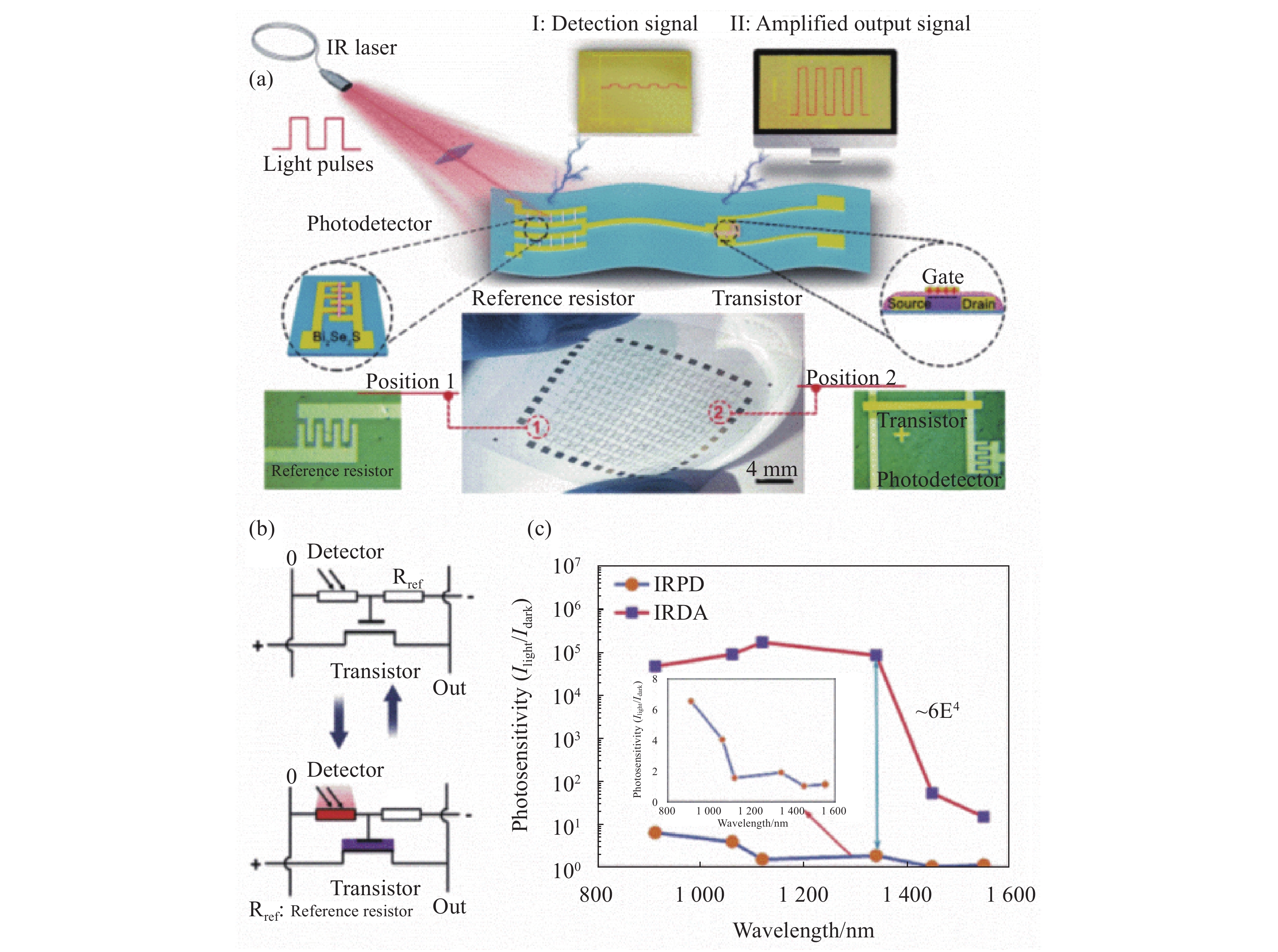
除此之外,光敏性是红外探测器与图像传感器十分重要的参数,可以决定最终成像的质量的对比度等。最近,G. Z. Shen组报道了一个简单的高度集成的红外探测放大系统(IRDA)。如图7(a)所示,该装置由光敏型Bi2Se2S纳米线作为红外探测电阻与参考电阻材料,具有较小亚阈值摆幅的n沟道耗尽型的Ga掺杂In2O3纳米线FET作为放大功能器件,In2O3纳米线晶体管的栅极连接红外探测电阻与参考电阻的共同电极。其机理如图7(b)所示,光照之前,Bi2Se2S纳米线载流子浓度低,探测电阻与参考电阻处于高阻态,共同电极输出一个大绝对值的负压,In2O3纳米线晶体管处于off态,源端输出电流极低;光照之后,光生电子-空穴对提高Bi2Se2S纳米线载流子浓度,降低探测电阻阻抗,而黑暗中的参考电阻依然处于高阻态,探测电阻分压路电流变大,共同电极电压增大,输出一个小绝对值的负压,In2O3纳米线晶体管处于on态,源端有一个大的输出电流。如图7(c)所示,该红外探测放大系统在1 342 nm光照下有着高达7.6×10⁴的室温光敏度,高于普通Bi2Se2S纳米线红外探测器几倍,并且高于所有已被报道的相似低维材料红外探测系统。该红外探测放大系统阵列可被制作在柔性聚对苯二甲酸乙二醇酯(PET)衬底上用于红外图像成像,在红外探测方面降低噪声,加强对比,简化电路有着巨大的前景[56]。

图 7 (a)红外探测放大系统结构示意图;(b)光照前后器件电路示意图;(c)红外探测放大器件与单根Bi2Se2S纳米线探测器光敏性随入射光波长变化对比[56]
Figure 7. (a) Schematic diagram of IRDA amplifing system; (b) Circuit schematic illustrations of switching mechanism analysis before and after illumination; (c) Comparison of photosensitivity for an IRDA system and single Bi2Se2S NW IRPD under different wavelengths[56]
以上为文中所介绍的不同构型的纳米线红外探测器。总的来说,二元化合物纳米线制备技术相对容易,不存在组分均匀性问题[57],然而探测范围却受材料带隙限制,不可调节;三元合金纳米线可以有效解决这个问题,通过控制组份调节禁带宽度,实现宽谱段红外探测[42],然而探测性能却更大程度取决于材料本身;异质结纳米线有望通过引入能带势垒降低暗电流或增加光电流进一步提高探测性能,并实现多场景应用如量子点、量子阱探测器等[58],还能钝化纳米线表面降低表面态影响,然而纳米线异质结外延材料生长过程中极易产生缺陷,其制备工艺仍然是一个较大的挑战;外场调控可以在不改变纳米线的情况下,充分利用纳米线表面态大幅提高光电探测性能,操作简单有效,然而更多的研究需要被投入以扩大其适用范围[9, 54-55];为了提高探测性能,实现探测器件小型化,红外系统的高度集成应运而生,在如成像、能量采集、感光等实际应用场景中有着非常重要的意义[26, 56],也有着非常广阔的发展前景,未来需要更多的投入设计并实现更加高性能、小型化等红外探测芯片。
-
文中主要介绍了半导体纳米线红外探测器,简述了纳米线材料的基本特性、材料选择与制备方法,并从二元化合物、三元合金、异质结、外场调控以及光电器件集成等方面分类总结了纳米线在红外光电探测器领域的最新进展。尽管最近几年关于纳米线红外探测器的研究不断取得突破,性能不断提升,然而仍然存在着一些需要解决的问题,比如暗电流较大的问题;中红外至远红外低探测率的问题;高质量纳米线制备的问题,以及纳米线器件稳定性的问题,除此之外,虽然目前纳米线生长方法成本低,产量高,然而一维材料的大面积集成定位问题,使其难以应用到实际生产当中。
为解决以上难题,未来可从以下几个方面入手:寻求新材料、发现新特性、设计新结构的器件;提高纳米线生长质量,减少缺陷对纳米线光电性能的损害;通过异质结合、修饰调控、表面钝化等多种方式进一步抑制暗电流,提高光电探测器的性能。总的来说,纳米线光电探测器在未来有着很好的发展和应用前景。
Recent advances in semiconductor nanowires infrared photodetectors (Invited)
-
摘要: 近年来,红外探测器由于其在军民领域广阔的应用前景已经受到了越来越多的关注。为了进一步实现室温宽谱段、高灵敏度、快速响应以及低功耗的红外探测器,低维半导体作为极具潜力的新型沟道材料得到了广泛的研究。其中,纳米线有着独特的电学与光电特性,当被应用到红外光电探测器中时,展现出了巨大的优势,例如尺寸小、功耗低、光吸收效率高、表面态丰富、易于光电子分离与收集以及与传统硅基工艺兼容等等。当前,对于纳米线红外探测器的研究一直在进行中并不断取得突破。文中主要概述了纳米线在红外光电探测领域的最新研究进展,介绍了半导体纳米线的基本特性、材料选择和制备方法,展示了多种二元与三元化合物半导体中已实现红外探测的纳米线材料及其当前研究达到的探测水平,并且分类总结了多种进一步提高光电探测性能的方法,包括异质结合、外场调控、器件集成等,随后针对不同构型纳米线红外探测器的优缺点,进行了简要的对比与说明,最后基于该领域仍然面临的挑战对其未来的发展方向进行了展望,并为其技术发展路线提出了初步的建议。Abstract: In recent years, infrared photodetectors have attracted increasing interest due to their promising applications in both military and civil areas. To further realize room-temperature, wide-spectrum, high-sensitivity, fast-response and low-power consumption infrared photodetectors, low-dimension semiconductors are considered as potential channel materials and have been studied widely. Among them, nanowires have special electrical and photoelectrical characteristics, showing enormous advantages in the applications of infrared photodetectors such as small size, low power consumption, high light absorption efficiency, abundant surface states, outstanding ability to separate and collect photoelectrons, good compatibility with Si complementary metal-oxide-semiconductor (CMOS) technology and so on. At present, nanowires infrared photodetectors are going through continuous progress and breakthrough. In this review, recent advances in semiconductor nanowires infrared photodetectors were outlined in details. At the beginning, the basic characteristics, material choice and preparation methods of nanowires were introduced. Subsequently, many nanowires including binary and ternary compound semiconductors for the use of infrared detection were presented and their current detectable levels were illustrated precisely. Many methods of further improving their detecting performances were also classified and summarized, including constructing heterostructures, applying external field and integrating with other functional devices. On the basis of the above-mentioned advances, a comparison of advantages and disadvantages among different nanowires infrared detectors was given. In the end, the future development trend was indicated based on the challenges in this area and preliminary suggestions for the technical development route were presented.
-
Key words:
- infrared photodetectors /
- nanowires /
- controllable growth /
- heterostructures /
- external field control
-

图 2 (a) CVD装置示意图[15];(b) 纳米线VLS和VSS生长机理示意图[34];(c) 传统纳米线生长与表面活性剂辅助纳米线生长机理示意图[17]
Figure 2. (a) Schematic representation of the CVD setup[15]; (b) Schematic illustration of the VLS and VSS growth mechanism[34]; (c) Schematic illustration of the conventional and the surfactant-assisted nanowire (NW) growth mode[17]
图 3 (a),(b) SnSe与SnS纳米线830 nm光探测器光响应时间[24];(c),(d) Sn催化生长的GaSb纳米线阵列1550 nm光探测器的光响应时间以及光电流与响应度随入射光功率变化关系[18]
Figure 3. (a),(b) Response time for 830 nm IR detectors based on SnSe and SnS NW[24]; (c),(d) Photocurrent response time as well as the photocurrent and responsivity versus illumination power of parallel array Sn-catalyzed GaSb NWs for a 1550 nm IR photodetector[18]
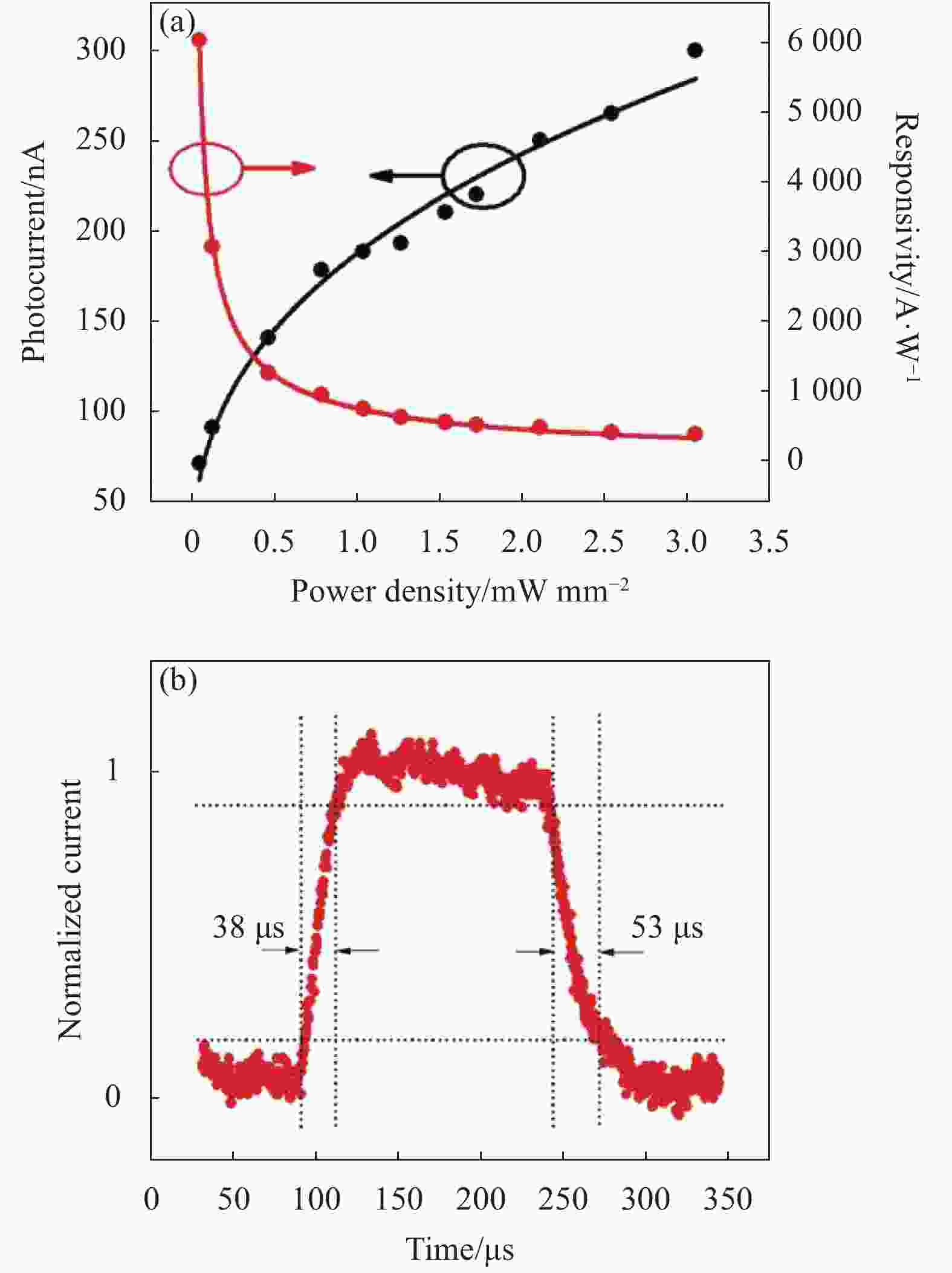
图 5 (a) PbSe-CsPbBr3纳米线光探测器随脉冲光变化的光电流[44];(b) GaAs/AlGaAs/GaAs纳米线沟道SEM图以及能带机理图[45];(c) InP-InAs二极管阵列光响应度与外量子效率随入射光波长的变化关系[23];(d) GaAs1−xSbx/InAs核-壳纳米线光探测器响应度随入射光波长变化关系[47];(e)肖特基-欧姆接触的InAs纳米线光探测器光照前后Ids-Vds曲线变化[22];(f) Au纳米颗粒-InAs异质结纳米线与InAs纳米线FET转移特性曲线对比[22]
Figure 5. (a) Time-dependent response of the photodetectors based on PbSe-CsPbBr3 heterostructure NWs[44]; (b) SEM image and the corresponding energy band alignment diagram of the single GaAs/AlGaAs/GaAs NW photodetector[45]; (c) Wavelength-dependent responsibility and EQE of InP-InAs photodiode arrays[23]; (d) Wavelength-dependent responsibility of the GaAs1−xSbx /InAs core−shell NW device[47]; (e) Ids-Vds curves before and after illumination of the Schottky-Ohmic contacted InAs NW photodetectors[22]; (f) Ids-Vgs curves of InAs nanowires with and without Au particles[22]
图 6 (a),(b)可见光辅助InAs纳米线探测器原理及其在不同波长红外光下的Ids-Vds曲线[9];(c)~(f) InAs纳米线场效应晶体管在铁电聚合物剩余极化态向上和向下时的Ids-Vds曲线及其结构与原理示意图、以及在3.5 μm光照下的光电流与响应度随入射光功率变化关系,4.3 μm光照下光电流随脉冲光变化关系[54];(g),(h) 表面态调控的InAs纳米线探测器光电导增益与响应度随Vbg变化关系及其原理示意图[55]
Figure 6. (a),(b) Energy band alignment diagram and Ids-Vds curve under IR light with different wavelengths of visible light-assisted InAs NW photodetectors[9]; (c)-(f) Schematic diagram and Ids-Vds curves of the InAs NW FETs with polarized upward state and polarized downward state of P(VDF-TrFE) film, their photocurrent and responsivity versus illumination power under 3.5 μm illumination and the time-dependent response under 4.3 μm illumination[54]; (g),(h) Logarithmic gain−Vbg characteristics and responsivity−Vbg characteristics as well as its mechanism diagram of surface-states-modulated InAs NW phototransistor[55]
图 7 (a)红外探测放大系统结构示意图;(b)光照前后器件电路示意图;(c)红外探测放大器件与单根Bi2Se2S纳米线探测器光敏性随入射光波长变化对比[56]
Figure 7. (a) Schematic diagram of IRDA amplifing system; (b) Circuit schematic illustrations of switching mechanism analysis before and after illumination; (c) Comparison of photosensitivity for an IRDA system and single Bi2Se2S NW IRPD under different wavelengths[56]
-
[1] 范晋祥, 杨建宇. 红外成像探测技术发展趋势分析[J]. 红外与激光工程, 2012, 41(12): 3145-3153. doi: 10.3969/j.issn.1007-2276.2012.12.003 Fan Jinxiang, Yang Jianyu. Development trends of infrared imaging detecting technology [J]. Infrared and Laser Engineering, 2012, 41(12): 3145-3153. (in Chinese) doi: 10.3969/j.issn.1007-2276.2012.12.003 [2] Rogalski A. HgCdTe infrared detector material: History, status and outlook [J]. Reports on Progress in Physics, 2005, 68(10): 2267-2336. [3] Grein C H, Young P M, Flatte M E, et al. Long wavelength InAs/InGaSb infrared detectors: Optimization of carrier lifetimes [J]. Journal of Applied Physics, 1995, 78(12): 7143-7152. [4] Levine B F. Quantum-well infrared photodetectors [J]. Journal of Applied Physics, 1993, 74(8): R1-R81. [5] Shen L, Pun E Y B, Ho J C. Recent developments in III-V semiconducting nanowires for high-performance photodetectors [J]. Materials Chemistry Frontiers, 2017, 1(4): 630-645. [6] Li Z, Allen J, Allen M, et al. Review on III-V semiconductor single nanowire-based room temperature infrared photodetectors [J]. Materials, 2020, 13(6): 1400. [7] 黄庆红. 国际半导体技术发展路线图(ITRS)2013版综述[J]. 中国集成电路, 2014, 23(9): 25-45. doi: 10.3969/j.issn.1681-5289.2014.09.002 Huang Q. International technology roadmap for semiconductors (ITRS) (2013 edition) [J]. China Integrated Circult, 2014, 23(9): 25-45. (in Chinese) doi: 10.3969/j.issn.1681-5289.2014.09.002 [8] Xia Y N, Yang P D, Sun Y G, et al. One-dimensional nanostructures: Synthesis, characterization, and applications [J]. Advanced Materials, 2003, 15(5): 353-389. [9] Fang H, Hu W, Wang P, et al. Visible light-assisted high-performance mid-infrared photodetectors based on single InAs nanowire [J]. Nano Letters, 2016, 16(10): 6416-6424. [10] Zhuge F, Zheng Z, Luo P, et al. Nanostructured materials and architectures for advanced infrared photodetection [J]. Advanced Materials Technologies, 2017, 2(8): 1700005. [11] Liang F X, Wang J Z, Li Z P, et al. Near-infrared-light photodetectors based on one-dimensional inorganic semiconductor nanostructures [J]. Advanced Optical Materials, 2017, 5(14): 1700081. [12] Luo L B, Zeng L H, Xie C, et al. Light trapping and surface plasmon enhanced high-performance NIR photodetector [J]. Scientific Reports, 2014, 4: 3914. [13] Yang Y, Wang X, Wang C, et al. Ferroelectric enhanced performance of a GeSn/Ge dual-nanowire photodetector [J]. Nano Letters, 2020, 20(5): 3872-3879. [14] Wu Y, Yan X, Zhang X, et al. A monolayer graphene/GaAs nanowire array schottky junction self-powered photodetector [J]. Applied Physics Letters, 2016, 109(18): 183101. [15] Yang Z X, Wang F, Han N, et al. Crystalline GaSb nanowires synthesized on amorphous substrates: From the formation mechanism to p-channel transistor applications [J]. ACS Applied Materials & Interfaces, 2013, 5(21): 10946-10952. [16] Yang Z X, Liu L Z, Yip S P, et al. Complementary metal oxide semiconductor-compatible, high-mobility, < 111 > -oriented GaSb nanowires enabled by vapor-solid-solid chemical vapor deposition [J]. ACS Nano, 2017, 11(4): 4237-4246. [17] Yang Z X, Han N, Fang M, et al. Surfactant-assisted chemical vapour deposition of high-performance small-diameter GaSb nanowires [J]. Nature Communications, 2014, 5: 5249. [18] Sun J, Peng M, Zhang Y, et al. Ultrahigh hole mobility of Sn-catalyzed GaSb nanowires for high speed infrared photodetectors [J]. Nano Letters, 2019, 19(9): 5920-5929. [19] Kuo C H, Wu J M, Lin S J, et al. High sensitivity of middle-wavelength infrared photodetectors based on an individual InSb nanowire [J]. Nanoscale Research Letters, 2013, 8: 327. [20] Sun J, Yin Y, Han M, et al. Nonpolar-oriented wurtzite InP nanowires with electron mobility approaching the theoretical limit [J]. ACS Nano, 2018, 12(10): 10410-10418. [21] Guo N, Hu W, Liao L, et al. Anomalous and highly efficient InAs nanowire phototransistors based on majority carrier transport at room temperature [J]. Advanced Materials, 2014, 26(48): 8203-8209. [22] Miao J, Hu W, Guo N, et al. Single InAs nanowire room-temperature near-infrared photodetectors [J]. ACS Nano, 2014, 8(4): 3628-3635. [23] Ren D, Meng X, Rong Z, et al. Uncooled photodetector at short-wavelength infrared using InAs nanowire photoabsorbers on InP with p-n heterojunctions [J]. Nano Letters, 2018, 18(12): 7901-7908. [24] Zheng D, Fang H, Long M, et al. High-performance near-infrared photodetectors based on p-type SnX (X = S, Se) nanowires grown via chemical vapor deposition [J]. ACS Nano, 2018, 12(7): 7239-7245. [25] Zheng D, Wang J, Hu W, et al. When nanowires meet ultrahigh ferroelectric field-high-performance full-depleted nanowire photodetectors [J]. Nano Letters, 2016, 16(4): 2548-2555. [26] Casadei A, Alarcon Llado E, Amaduzzi F, et al. Polarization response of nanowires a la carte [J]. Scientific Reports, 2015, 5: 7651. [27] Zhai T, Fang X, Liao M, et al. A comprehensive review of one-dimensional metal-oxide nanostructure photodetectors [J]. Sensors, 2009, 9(8): 6504-6529. [28] Soci C, Zhang A, Bao X Y, et al. Nanowire photodetectors [J]. Journal of Nanoscience and Nanotechnology, 2010, 10(3): 1430-1449. [29] Hu J T, Odom T W, Lieber C M. Chemistry and physics in one dimension: Synthesis and properties of nanowires and nanotubes [J]. Accounts of Chemical Research, 1999, 32(5): 435-445. [30] Rogalski A, Martyniuk P, Kopytko M. InAs/GaSb type-II superlattice infrared detectors: Future prospect [J]. Applied Physics Reviews, 2017, 4(3): 031304. [31] Sun J, Han M, Gu Y, et al. Recent advances in group III-V nanowire infrared detectors [J]. Advanced Optical Materials, 2018, 6(18): 1800256. [32] Gao Z, Sun J, Han M, et al. Recent advances in Sb-based III-V nanowires [J]. Nanotechnology, 2019, 30(21): 212002. [33] Peng K, Lu A, Zhang R, et al. Motility of metal nanoparticles in silicon and induced anisotropic silicon etching [J]. Advanced Functional Materials, 2008, 18(19): 3026-3035. [34] Lensch-Falk J L, Hemesath E R, Perea D E, et al. Alternative catalysts for VSS growth of silicon and germanium nanowires [J]. Journal of Materials Chemistry, 2009, 19(7): 849-857. [35] Morkoetter S, Funk S, Liang M, et al. Role of microstructure on optical properties in high-uniformity In1-xGaxAs nanowire arrays: Evidence of a wider wurtzite band gap [J]. Physical Review B, 2013, 87(20): 205303. [36] Wang J F, Gudiksen M S, Duan X F, et al. Highly polarized photoluminescence and photodetection from single indium phosphide nanowires [J]. Science, 2001, 293(5534): 1455-1457. [37] Nainani A, Bennett B R, Boos J B, et al. Enhancing hole mobility in III-V semiconductors [J]. Journal of Applied Physics, 2012, 111(10): 103706. [38] Ren P, Hu W, Zhang Q, et al. Band-selective infrared photodetectors with complete-composition-range InAsxP1-x alloy nanowires [J]. Advanced Materials, 2014, 26(44): 7444-7449. [39] Ren D, Azizur-Rahman K M, Rong Z, et al. Room-temperature midwavelength infrared InAsSb nanowire photodetector arrays with Al2O3 passivation [J]. Nano Letters, 2019, 19(5): 2793-2802. [40] Li Z, Yuan X, Gao Q, et al. In situ passivation of GaAsSb nanowires for enhanced infrared photoresponse [J]. Nanotechnology, 2020, 31(24): 244002. [41] Zhou C, Zhang X T, Zheng K, et al. Self-assembly growth of In-rich InGaAs core-shell structured nanowires with remarkable near-infrared photoresponsivity [J]. Nano Letters, 2017, 17(12): 7824-7830. [42] Li D, Lan C, Manikandan A, et al. Ultra-fast photodetectors based on high-mobility indium gallium antimonide nanowires [J]. Nature Communications, 2019, 10: 1664. [43] Guo P, Hu W, Zhang Q, et al. Semiconductor alloy nanoribbon lateral heterostructures for high-performance photodetectors [J]. Advanced Materials, 2014, 26(18): 2844-2849. [44] Fan C, Xu X, Yang K, et al. Controllable epitaxial growth of core-shell PbSe@CsPbBr3 wire heterostructures [J]. Advanced Materials, 2018, 30(45): 1804707. [45] Zhu X, Lin F, Zhang Z, et al. Enhancing performance of a GaAs/AlGaAs/GaAs nanowire photodetector based on the two-dimensional electron-hole tube structure [J]. Nano Letters, 2020, 20(4): 2654-2659. [46] Ma L, Hu W, Zhang Q, et al. Room-temperature near-infrared photodetectors based on single heterojunction nanowires [J]. Nano Letters, 2014, 14(2): 694-698. [47] Ni Z, Wang H, Zhao Q, et al. Ambipolar conjugated polymers with ultrahigh balanced hole and electron mobility for printed organic complementary logic via a two-step c-h activation strategy [J]. Advanced Materials, 2019, 31(10): 1806010. [48] Fang H, Hu W. Photogating in low dimensional photodetectors [J]. Advanced Science, 2017, 4(12): 1700323. [49] Han Y, Fu M, Tang Z, et al. Switching from negative to positive photoconductivity toward intrinsic photoelectric response in InAs nanowire [J]. ACS Applied Materials & Interfaces, 2017, 9(3): 2867-2874. [50] Alexander-Webber J A, Groschner C K, Sagade A A, et al. Engineering the photoresponse of InAs nanowires [J]. ACS Applied Materials & Interfaces, 2017, 9(50): 43993-44000. [51] Li J, Yan X, Sun F, et al. Anomalous photoconductive behavior of a single InAs nanowire photodetector [J]. Applied Physics Letters, 2015, 107(26): 263103. [52] Zhang X, Li Z, Yao X, et al. Light-induced positive and negative photoconductances of InAs nanowires toward rewritable nonvolatile memory [J]. ACS Applied Electronic Materials, 2019, 1(9): 1825-1831. [53] Yang Y, Peng X, Kim H S, et al. Hot carrier trapping induced negative photoconductance in InAs nanowires toward novel nonvolatile memory [J]. Nano Letters, 2015, 15(9): 5875-5882. [54] Zhang X, Huang H, Yao X, et al. Ultrasensitive mid-wavelength infrared photodetection based on a single InAs nanowire [J]. ACS Nano, 2019, 13(3): 3492-3499. [55] Zhang X, Yao X, Li Z, et al. Surface-states-modulated high-performance InAs nanowire phototransistor [J]. Journal of Physical Chemistry Letters, 2020, 11(15): 6413-6419. [56] Ran W, Wang L, Zhao S, et al. An integrated flexible all-nanowire infrared sensing system with record photosensitivity [J]. Advanced Materials, 2020, 32(16): 1908419. [57] 吕衍秋, 鲁星, 鲁正雄, 等. 锑化物红外探测器国内外发展综述[J]. 航空兵器, 2020, 27(5): 1-12. Lv Yanqiu, Lu Xing, Lu Zhengxiong, et al. Review of antimonide infrared detector development at home and abroad [J]. Aero Weaponry, 2020, 27(5): 1-12. (in Chinese) [58] Spies M, Monroy E. Nanowire photodetectors based on wurtzite semiconductor heterostructures [J]. Semiconductor Science and Technology, 2019, 34(5): 053002. -

 点击查看大图

计量
- 文章访问数: 967
- HTML全文浏览量: 328
- PDF下载量: 204
- 被引次数: 0

