


 下载:
下载:


-
红外探测技术具有无源探测、抗干扰能力强等特点,在各个领域有着极其重要的应用。其中,3~5 μm中红外波段是一个非常重要的大气窗口,在公共场所成像测温、森林火灾预警、医疗诊断、天文观测、夜视安防以及预警与跟踪等领域有着重要应用,成为当今世界各国竞相发展的重要技术。
高性能的制冷型红外探测器材料主要包括HgCdTe(MCT)[1]、InSb体材料[2]、Sb化物II类超晶格和量子阱探测器等。II-VI族半导体 HgCdTe是目前性能最优的红外探测器材料。在几乎晶格匹配的CdZnTe衬底上生长的HgCdTe探测器可以实现1~15 μm连续截止波长覆盖,同时具备高量子效率和低暗电流,但受外延尺寸限制,在大面阵领域应用具备一定劣势。InSb焦平面探测器具有大面阵、均匀性高、稳定性好等特点,目前在中波红外探测器系统中占据主导地位,但是InSb焦平面探测器的工作温度被限制在110 K左右,难以实现高温工作[3]。在晶格匹配的GaSb衬底上生长的Sb化物II类超晶格材料经过多年发展,成为国际上研发新一代高性能焦平面芯片的重要材料体系。以InAs、GaSb、AlSb异质结构建的II类超晶格材料,可以充分利用其晶格匹配的条件,灵活设计其能带结构,使器件的响应光谱覆盖整个红外波段范围。Sb化物II类超晶格材料同时具有俄歇复合率低、电子有效质量大、材料均匀性好等特点[4]。其中,InAs/GaSb超晶格是最早研究的II类超晶格结构,基于该结构的Sb化物焦平面性能迅速提升,已接近或超过MCT和InSb探测器。然而,传统的InAs/GaSb超晶格材料少数载流子寿命较短,限制了器件性能的进一步提升。近年来,研究人员将目光转向了无Ga型的InAs/InAsSb超晶格材料,InAs/InAsSb超晶格结构避免了Ga原子带来的自身缺陷,具有更长的载流子寿命。因此,InAs/InAsSb超晶格材料是高工作温度中波红外探测器的理想解决方案之一。
提高红外探测器工作温度的关键在于降低器件的暗电流、提高器件的量子效率。研究人员除了在能带结构及材料生长领域进行不断的研究工作及性能优化之外,器件制备领域也是一个重要的优化方向。其中,使用多种光学微纳结构,是实现量子效率提升的一个重要途径。通过器件表面微结构的制备,可以提高器件的吸收效率,进而降低吸收区厚度、材料缺陷、暗电流,实现高工作温度中红外探测。
文中瞄准中红外波段InAs/InAsSb超晶格探测器及光子晶体结构,结合笔者课题组近年来在该领域的研究成果,详细介绍了两种提高中红外探测器性能的方案及国内外的研究进展。
-
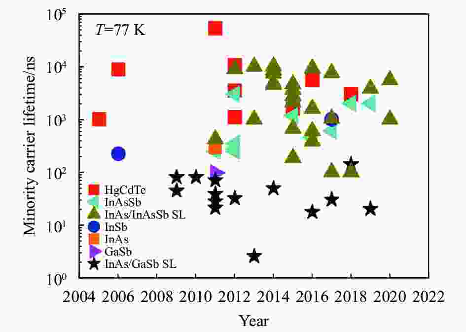
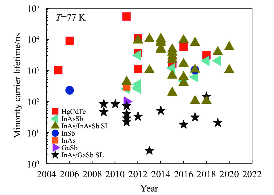
目前的研究结果表明,中波和长波InAs/GaSb超晶格焦平面在不高于150 K和70 K的温度下,其NEDT与HgCdTe焦平面接近。然而,受制于InAs/GaSb超晶格材料中极低的少子寿命,其性能并未接近理论极限。具体来说,InAs/GaSb超晶格中存在着严重的SRH复合,复合中心的能级越接近禁带中央时,SRH复合几率越大。研究发现,与Ga有关的本征缺陷在禁带中心附近引入了缺陷能级形成的复合中心是导致SRH机制主要原因。于是,无Ga型的InAs/InAsSb超晶格结构被提出[5]。图1所示了近年来各研究机构报道的无Ga型II超晶格、HgCdTe、InAs/GaSb二类超晶格及其他III-V族红外探测器在77 K温度时的少数载流子寿命。目前,长波InAs/InAsSb 超晶格在77 K的少子寿命达到了412 ns[6],中波InAs/InAsSb超晶格在15 K时的少子寿命更是达到了12.8 µs[7-8],比InAs/GaSb II类超晶格高出了一个数量级。
与InAs/GaSb II类超晶格材料相似,InAs/InAsSb通过改变超晶格的周期厚度以及InAsSb中的Sb元素组分,实现器件截止波长的改变。对于固定截止波长的InAs/InAsSb材料,通过InAsSb层的压应变补偿InAs层张应变的方法,实现晶格的应变平衡。然而,在长波红外材料领域,InAs/InAsSb材料长波吸收效率更低、空穴迁移限制更高,因此InAs/InAsSb材料在长波材料应用领域优势并不明显[10]。
与更成熟的InAs/GaSb II类超晶格相比,InAs/InAsSb II类超晶格生长相对容易。图2展示了InAs/GaSb II类超晶格和InAs/InAsSb II类超晶格生长中使用的分子束外延(MBE)快门序列。原则上,InAs/InAsSb II类超晶格的生长只涉及打开和关闭Sb快门,In和As快门可以在整个过程中保持打开,而在InAs/GaSb超晶格生长中需要使用四个快门。因此,InAs/InAsSb超晶格结构的应变平衡与界面控制难度更低[11]。
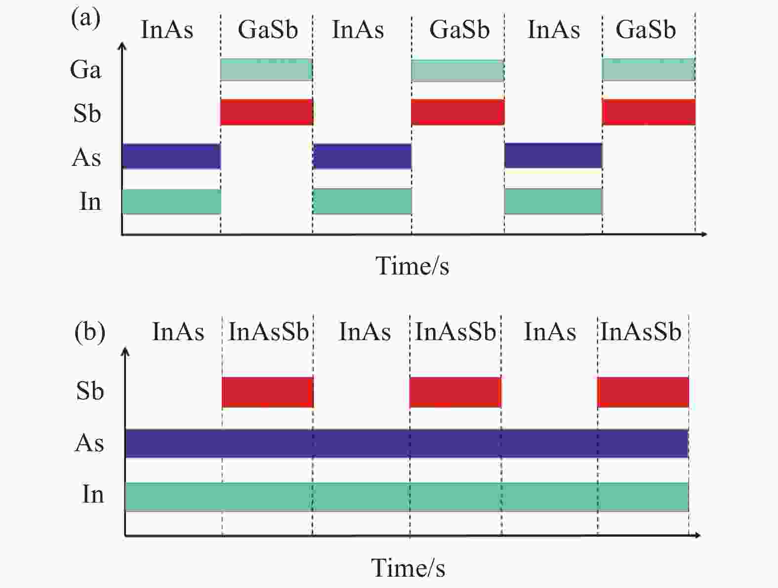
图 2 (a) InAs/GaSb II类超晶格材料与(b) InAs/InAsSb II类超晶格材料分子束外延生长的快门控制
Figure 2. Shutter sequences used in MBE growth of (a) InAs/GaSb type-II superlattice (T2 SLs) and (b) InAs/InAsSb T2 SLs
InAs/InAsSb II类超晶格材料的分子束外延生长同样面对着诸多挑战。2013年,亚利桑那大学张永航教授团队对生长时的衬底温度和束流对生长质量及InAsSb层中的组分的影响进行了研究。研究表明,InAs/InAsSb超晶格中的应力显著影响着材料中的穿透位错,较低的生长温度有利于生长高质量的InAs/InAsSb超晶格材料[12]。同时,InAs-InAsSb界面处的Sb偏析和扩散,形成了缓变型界面。这种现象在InAsSb后外延InAs层形成的界面处更为明显。同时Sb偏析可以导致InAs/InAsSb超晶格探测器量子效率降低[13]。尽管InAs/InAsSb界面处有大量的共有原子,不需要引入额外的界面控制,但目前仍没有有效的改善和控制界面处Sb扩散和偏析问题的方法。
-
为了提供高质量的InAs/InAsSb超晶格材料,笔者课题组的研究人员对应用于中远红外波段的高Sb组分InAs/InAs0.5Sb0.5超晶格材料的分子束外延生长进行了深入研究。结合XRD、HRTEM、AFM测试手段,针对InAsSb层分子束外延的As/Sb束流比、生长温度、界面控制方法等进行了一系列研究工作。同时,针对InAs层中插入AlAs形成的InAlAs势垒结构,对该层AlAs生长速率、InAs/AlAs界面控制等进行了研究工作[14]。
对于InAs/InAsSb超晶格材料的外延生长,InAsSb层的Sb/As束流比是决定Sb组分的主要生长条件,Sb/As束流比可以通过XRD零级峰与一级卫星峰的间距来进行调整。图3(d)显示了卫星峰间距与Sb组分随Sb/As束流比变化趋势,Sb/As束流比通过固定As束流,改变Sb束流来调整,根据确定的As、Sb、In束流进行分子束外延生长,并对结果进行XRD测试,得到图3(e)所示的超晶格XRD曲线。样品的0级衍射峰位于−186'',表明InAs/InAsSb超晶格与GaSb衬底呈现正失配。0级峰的半峰宽为25'',超晶格摇摆曲线中卫星峰的半峰宽小于40'',四级卫星峰以内的半峰宽小于30'',卫星峰的排列表明,超晶格周期厚度为98 Å(1 Å=10-10 m),符合理论预期。

图 3 (a) InAs/AlAs/InAsSb II类超晶格势垒层能带结构; (b) InAs/InAsSb吸收层快门序列示意图; (c) InAs/AlAs/InAsSb势垒层快门序列示意图;(d) InAs/AlAs/InAsSb超晶格0级峰间距及Sb组分随Sb/As束流比变化曲线;(e) InAs/InAsSb超晶格材料高分辨率X射线衍射测试(蓝色)及模拟(红色)结果;(f)不同InAs/AlAs界面控制条件下5.6/2.2/5.6/7.5 mL InAs/AlAs/InAs/InAsSb超晶格材料各级卫星峰半峰宽[14]
Figure 3. (a) Band alignment of InAs/AlAs/InAsSb T2 SLs; (b) Shutter sequences used in InAs/InAsSb absorber growth; (c) Shutter sequences used in InAs/AlAs/InAsSb barrier growth; (d) The 0th diffraction peak and Sb component in InAs/AlAs/InAsSb SLs by varying the Sb/As flux ratio; (e) High-resolution X-ray diffraction (HRXRD) experimental (blue) and simulation (red) curve of the InAs/InAsSb SLs; (f) FWHM in HRXRD pattern of 5.6/2.2/5.6/7.5 mL InAs/AlAs/InAs/InAsSb SLs samples with different interfaces between InAs and AlAs layer[14]
由于InAs和AlAs材料之间有约6.5%的晶格失配,为了获得平整的超晶格材料,需要优化AlAs层的生长速率。若Al的生长速率过慢,则元素表面迁移时间过长,AlAs层由二维生长变成了岛状生长。提高Al的生长速度,表面逐渐呈现清晰的原子台阶,而当Al生长速率过快时,材料的表面粗糙度提高。研究表明AlAs层的分子束外延在0.3 mL/s附近存在较窄的生长窗口。
界面处的元素无序性和原子扩散是超晶格生长需要解决的一个重要问题,这一问题可以由 HRXRD 曲线衍射峰宽度标定。衍射峰变宽甚至分离表明 InAs/AlAs 界面产生了 InAlAs 等中间产物,产生这一现象的主要原因在于 InAs/AlAs 界面不均匀,且AlAs 层厚度的增加导致了界面粗糙[12]。另外,两种不同材料之间的扩散也是导致界面模糊的原因。通过使用多种界面控制方法——As浸润和生长中断法,进行超晶格结构的分子束外延生长,并进行HRXRD测试。发现采用3 s中断法和6 s As浸润界面控制方法时,中间产物 InAlAs 被消除。
根据 M.Arzberger 等人的理论[15],在InAs层中插入2.3 mL的AlAs层开始由层状结构转化为量子点局域生长模式,而插入2.2 mL的AlAs层的样品则保持层状生长,几乎没有量子点存在的迹象。因此,实验选取以0.3 mL/s进行AlAs层外延的5.6/2.2/5.6/8 mLsInAs/AlAs/InAs/InAs0.5Sb0.5超晶格材料样品。图4(a)所示为材料厚度符合设计值,且原子台阶清晰。但是由于 Sb 偏析的出现,InAs和InAsSb层之间的界面并非直线。平行于生长方向的几何向量分析该方向的应变张量εyy图像(图4(c))也印证了这一结论。这也为后续材料优化研究提供了方向。
-
InAs/InAsSb II类超晶格红外探测器通常使用nBn型器件结构。在该结构设计中,势垒层(Barrier, B)夹在n型接触层和吸收层之间。理想情况下,势垒结构的价带位置与吸收层对齐,不存在价带带阶。而导带中的带阶形成势垒,起到阻挡多数载流子传输的效果。与传统的p-i-n结构相比,nBn结构可以抑制产生-复合暗电流和表面漏电流,提高器件的工作温度。但是,在nBn势垒结构设计中,为了抑制扩散电流,会有意对n型接触层进行重掺杂,同时吸收层保持在低掺杂水平,这将导致吸收层和接触层之间的费米能级不同,出现一个空穴垒,导致探测器光响应的偏压依赖性,降低探测器性能[16]。针对于此,笔者课题组提出并深入研究了一种p+-B-n 势垒结构,并采用AlAsSb/InAsSb超晶格势垒,解决了探测器光响应的偏压依赖性问题[17]。
根据1.2节所述分子束外延优化方法,同样对5 μm截止波长,9/3 mLs InAs/InAs0.45Sb0.55晶格周期的材料质量进行了优化。Sb组分的提升进一步提高了器件的量子效率。势垒层使用具有相同 Sb 成分的AlAs0.45Sb0.55/ InAs0.45Sb0.55超晶格结构。吸收层及势垒层使用相同的Sb组分,可以降低材料外延生长的控制难度。器件能带结构如图5(c)所示,势垒层起到阻挡导带中电子输运的作用,同时价带中空穴的输运完全没有限制。这种结构使得p-n结耗尽区主要位于 p+接触层和势垒层内。与nBn型单极势垒结构相比,p+-B-n器件结构既保留了势垒型探测器的优势,降低了产生复合电流和表面漏电流。同时,类似于p-i-n光电二极管,探测器光响应具备极低的偏压依赖性。

图 5 (a) InAs/InAs0.45Sb0.55吸收区能带结构;(b) AlAs0.45Sb0.55/InAs0.45Sb0.55势垒层能带结构;(c) p+-B-n器件能带结构示意图;(d) p+-B-n器件暗电流密度在不同温度下随偏压变化曲线;(e)-100mV偏压下 p+-B-n器件暗电流密度随温度变化曲线[17]
Figure 5. (a) Band alignment of the InAs/InAs0.45Sb0.55 absorber; (b) Band alignment of the AlAs0.45Sb0.55/InAs0.45Sb0.55 barrier layer; (c) Schematic diagram of the p+-B-n device energy band structure; (d) Curves of dark current density with bias of the p+-B-n photodetectors at different temperature; (e) Dark current density of the p+-B-n photodetector under -100 mV applied bias [17]
研究工作经过一系列的分子束外延参数优化,使用高质量的外延材料完成了器件的制备,并对器件进行了电学和光学性能测试。测试结果表明,探测器在−100 mV 的偏置电压下光响应达到饱和,150 K器件的峰值响应度0.97 A/W, 量子效率为29%,探测器峰值波长为4.1 μm,器件暗电流密度为1.2×10⁻⁴ A/cm2。300 K时器件暗电流密度为0.1 A/cm2。通过对探测器暗电流密度与温度的变化关系进行拟合(图5(e)),在220~300 K温度范围内,暗电流密度随温度变化的激活能约为246 meV,与设计的InAs/InAs0.45Sb0.55吸收层带隙约250 meV一致,此时扩散电流是探测器暗电流的主要产生机制。100~200 K温度范围内的激活能为120 meV,约为吸收层带隙的一半,此时产生-复合电流成为主导。在低于100 K时,随着温度的降低,暗电流密度几乎保持不变,暗电流主要为隧穿电流及表面漏电流。150 K时器件峰值探测率D*为1.2×1011cm·Hz1/2/W,300 K时为3.8× 109 cm·Hz1/2/W。
-
除了采用能带调控方法提高Sb化物红外探测器性能之外,光学调控也是非常有效的一种方法。光学调控通常采用表面微纳结构,如光子晶体、陷光结构、表面等离子体增强等,调控入射光的空间分布。借助于多种微加工手段和图形转移技术,微结构的尺寸可以实现纳米级的精确控制。通过在红外探测器表面制备表面微纳结构,可以实现器件对红外光的吸收和响应谱变化。
近年来,国内外学者对于不同的光学结构设计进行了研究工作,如图6所示。2012年,美国桑迪亚国家实验室提出了一种金属纳米天线结构。纳米天线通过将入射平面波转换为更紧密结合和集中的表面波,提高了吸收效率,从而降低红外探测器吸收区厚度,减少了暗电流和串扰,提高了探测器性能。在该设计中金属尺寸仅为50 nm,纳米天线制备使用电子束曝光技术进行图形转移,且金属层厚度有所限制。该研究工作在不改变探测器性能的条件下,通过引入纳米天线,将吸收区厚度降低了一个数量级[21]。2018年,南洋理工大学报道了使用二维表面金属结构的室温中红外探测器,在InAsSb做为吸收区的红外探测器表面,制备二维亚波长金属孔洞结构。该金属孔洞结构通过电子束曝光技术制备。通过该结构改变了器件表面入射光的反射率,提高了器件的吸收效率。最终实现了室温探测率0.8×1010cm Hz1/2 W−1的优异性能[19]。2019年,美国海军实验室使用金属光栅将入射光耦合到横向传播的表面等离子体激元 (SPP) 模式,以增加有效吸收长度。该研究工作使用Ge金属光栅,尺寸同样在纳米量级,图形通过电子束曝光技术转移,制备的 SPP 共振的光栅扩展了吸收带,引入该结构可以将吸收区厚度降低5倍,将暗电流降低3~8倍[20]。
-
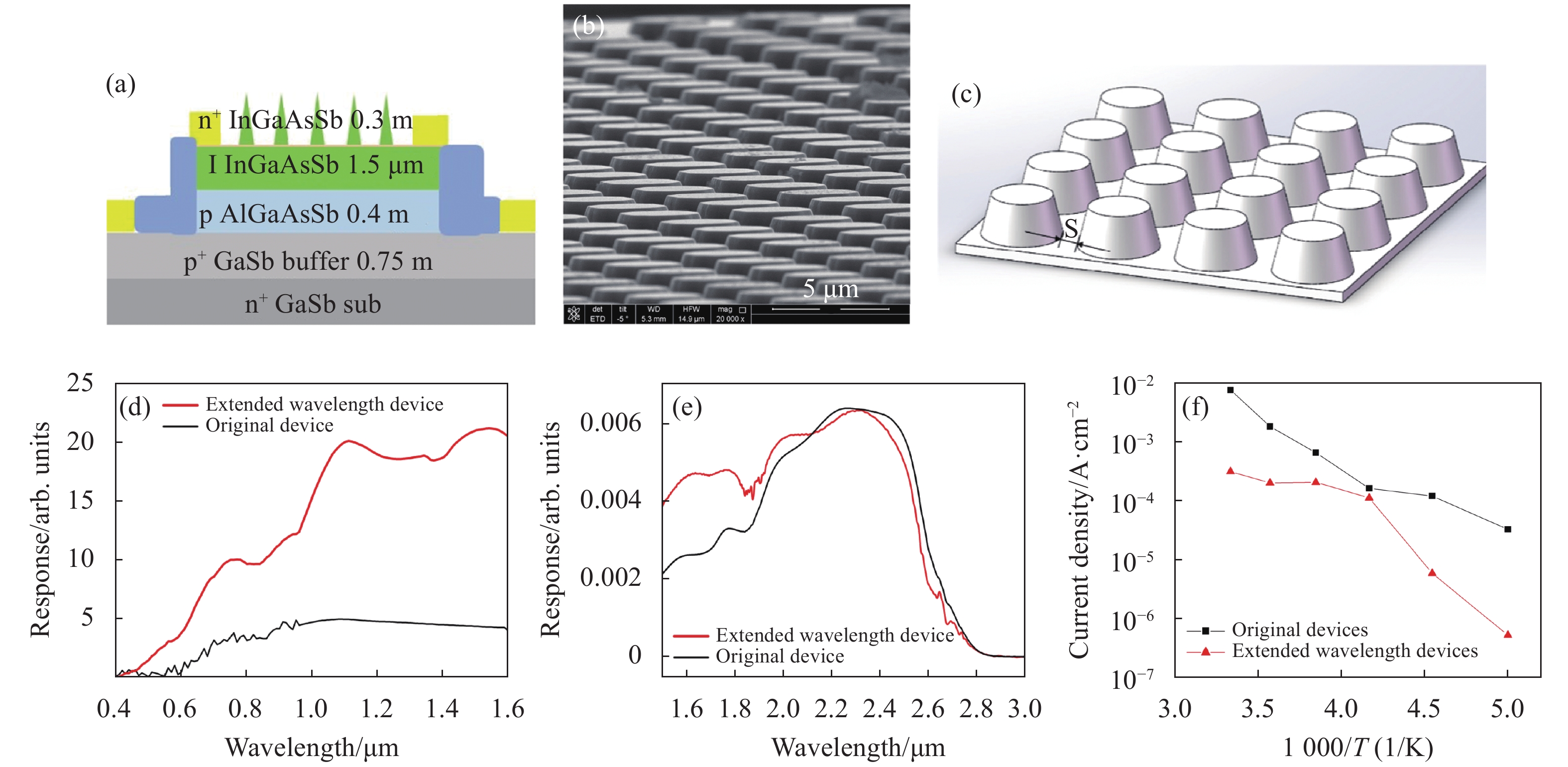
笔者课题组对陷光结构在Sb化物红外探测器中的应用于2016年展开了研究工作,使用了如图7所示的陷光结构阵列。这种结构于2011年由A. I. D’Souza等提出[22],通过使用一种锥形阵列周期性排布的金字塔阵列结构,减少吸收区对入射光的反射,增强探测器的吸收。在此基础上,将这种结构应用于生长在GaSb衬底上的pBn单极势垒探测器,将GaSb做为p型接触层,保证空穴在没有空穴势垒的条件下传输。将AlGaAsSb做为势垒层,InGaAsSb做为吸收层,并在其表面构建图7所示的光子陷阱结构。制备的器件实现了0.4 ~2.8 μm的宽光谱响应,且暗电流密度实现了两个数量级的下降,证明了这种结构实现高温探测的潜力[23]。

图 7 (a) InGaAsSb/AlGaAsSb光子陷阱探测器结构;(b)陷光结构扫描电子显微镜形貌;(c)陷光结构整体设计图;光子陷阱探测器(红色)及不带陷光结构的探测器(黑色)在(d) 400~1600 nm波段及(e) 1.5~3 μm波段响应度;(f)暗电流密度随温度变化曲线[23]
Figure 7. (a) Structure of InGaAsSb/AlGaAsSb photodiodes with photon-trap arrays; (b) SEM image off photon-trap arrays; (c) Design of photon-trap arrays;Response of the photodiodes with (red) and without (black) photon-trap arrays at (d) 400-1600 nm and (e) 1.5-3 μm; (f) Dark current density at different temperature [23]
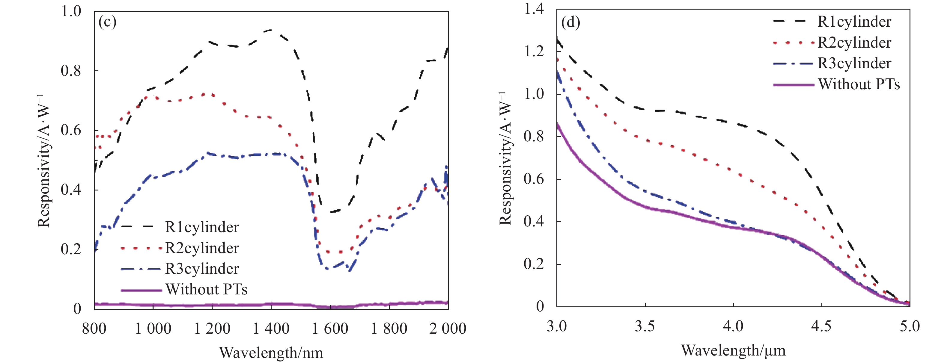
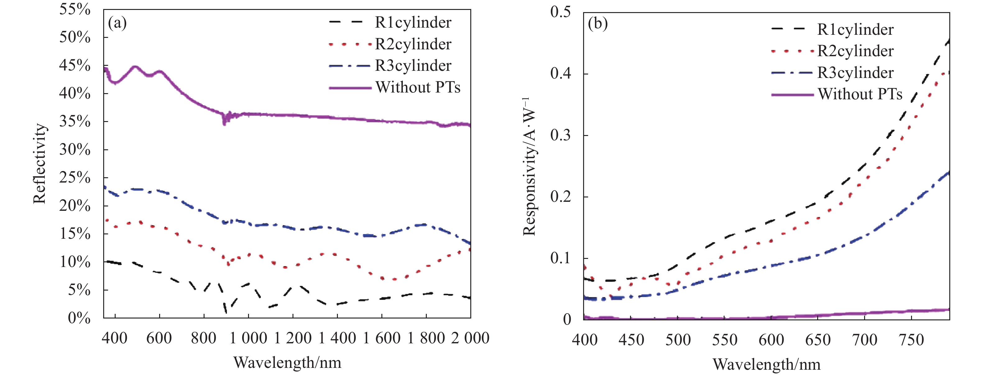
同样的结构被用于InAs/GaSb超晶格中波红外探测器件。针对不同尺寸的阵列结构进行了器件制备与测试工作。InAs/GaSb超晶格红外探测器采用nBn型能带结构,陷光结构制备于表面n型吸收区。如图8所示,陷光结构降低了样品表面对光的反射率,实现了400 nm~5 μm波段响应度的整体提升[24]。


-
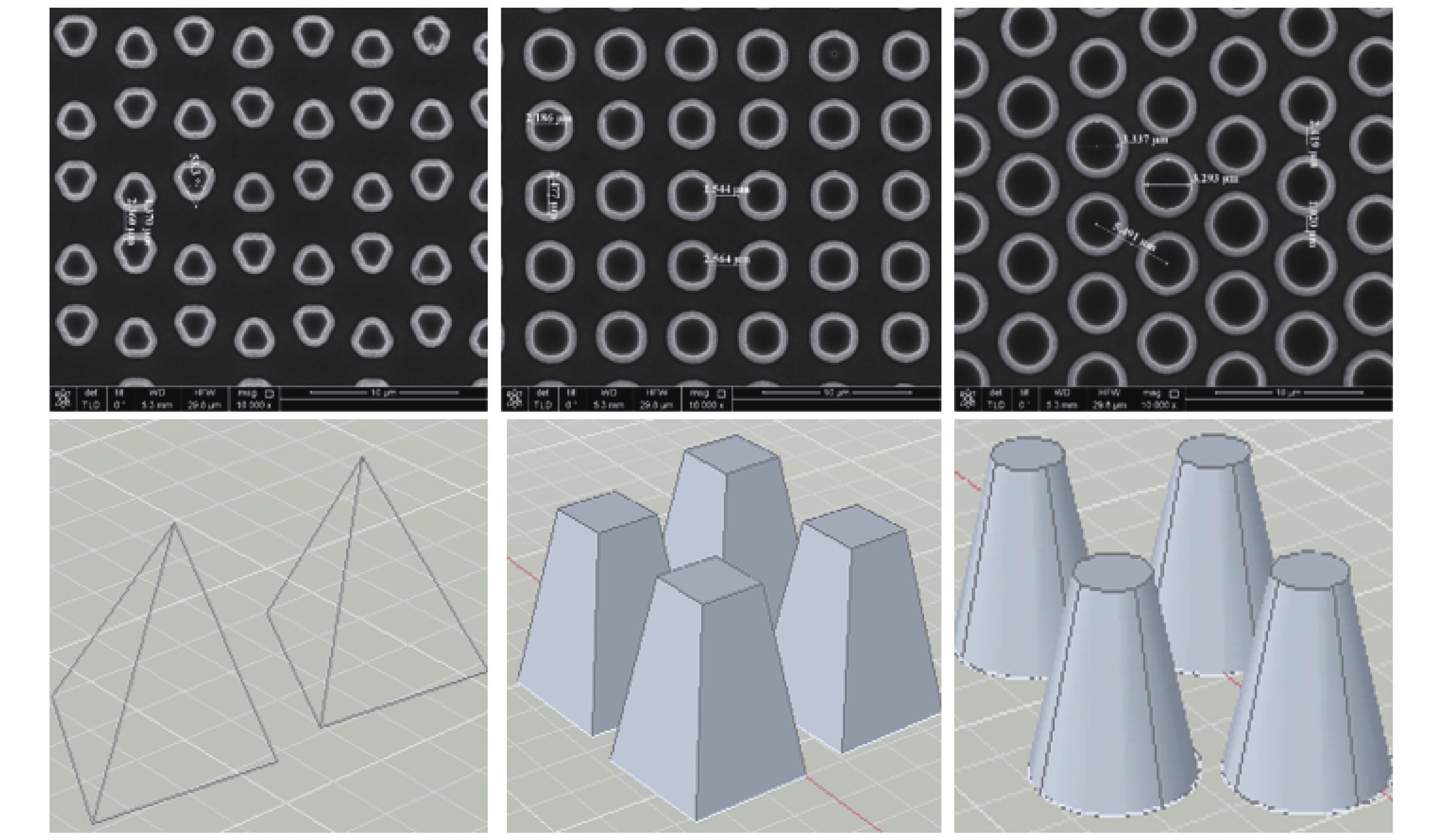
针对陷光结构形貌的研究工作表明,不同的光子陷阱结构对器件响应度的提升效果不同。通过对图9所示的四面体结构、金字塔结构、圆柱结构的光子陷阱的器件进行响应谱测试,结果表明金字塔结构具备更低的表面反射率和更高的响应度。这是由于光子进入吸收区后,在相邻的金字塔结构侧表面之间多次反射,直至光子被吸收,大大提高了光子的吸收面积。
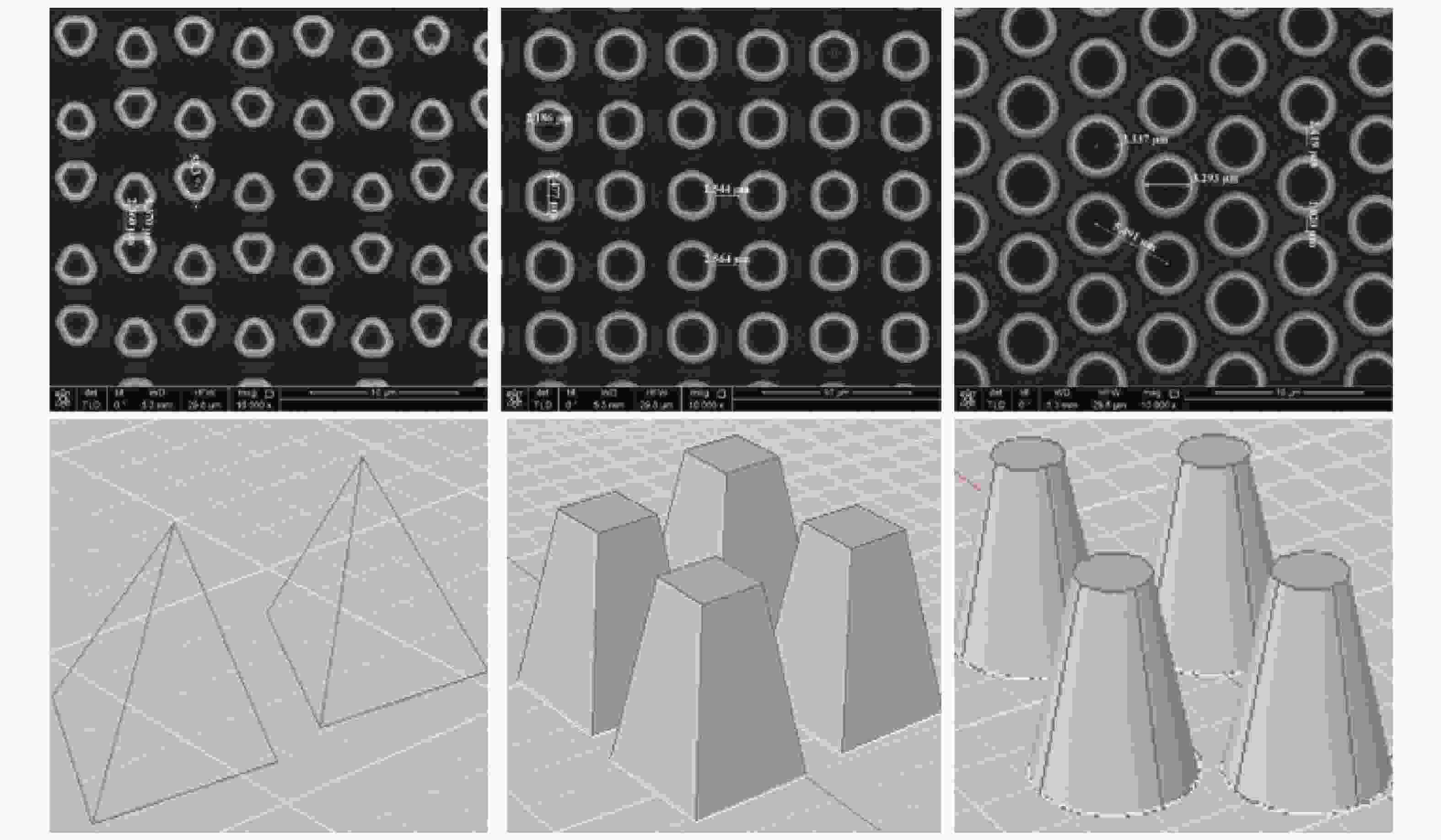
图 9 三种不同的光子晶体结构(四面体、金字塔、圆柱)
Figure 9. Three different kinds of photon-trap arrays (Tetrahedron, pyramid, cylinder)
针对这种可以实现侧壁反射增强的结构,对图10所示不同尺寸、孔洞及柱状结构对材料表面反射率的影响展开了研究工作。图10(c)计算了棱镜结构(红色)和孔洞结构(蓝色)的反射率随边长L从1.5~6 μm的变化的趋势。可以发现,当L小于4.8 μm时,边长小的柱状阵列探测器反射率小于孔洞探测器。同时,陷光结构尺寸越小,反射率越低,光吸收率越强。不同类型的陷光结构对应的尺寸优化方向有所区别[25]。

值得一提的是,该部分的器件制备过程中均使用标准光刻技术进行图形转移。使用电子束曝光(EBL)等更为精细的微纳器件加工工艺,无疑可以获得更优的探测率及响应度,但是同时也增加了器件的制备成本。因此,陷光结构红外探测器件可以根据不同应用需求,进行加工工艺的选择。
-
Sb化物II类超晶格材料是研发新一代高性能红外焦平面芯片的重要材料体系,无Ga型InAs/InAsSb超晶格材料具有少子寿命长、外延生长控制简单和缺陷容忍度高等特点,是实现高温工作中波红外探测器的优选材料体系。InAs/InAsSb超晶格红外探测器研究在短短几年时间内取得的快速进展,充分说明了InAs/InAsSb超晶格在实现高温工作探测器方面具有的发展潜力,但充分发挥该材料体系的优越性能仍然面临很大的技术挑战,例如:如何进一步提高InAs/InAsSb超晶格材料的吸收系数,如何向短波方向拓展该材料体系的截止波长以及如何发展有效可靠的器件钝化技术等等。未来InAs/InAsSb超晶格红外探测器仍具备较大的发展空间,包括:设计势垒型探测器结构,抑制探测器暗电流,进一步提高探测器工作温度;通过在器件表面制备微结构,提高器件的吸收效率;发展新型表面钝化技术,例如ALD沉积Al2O3材料等,抑制探测器表面漏电流等等。随着新型器件结构的创新、材料生长技术的优化和器件制备工艺的完善,相信Sb化物II类超晶格探测器性能将得到提高和稳定,在更多的应用领域展现其优异的性能。
Research progress of high performance Sb-based superlattice mid-wave infrared photodetector (Invited)
-
摘要: 中红外探测技术作为一种重要的被动探测手段,在各个领域都有着非常重要的作用。其中,以InAs/InAsSb超晶格材料为基础的无Ga型Sb化物II类超晶格探测器,由于去除了Ga原子的缺陷,具有更高的少子寿命,有利于提高探测器性能。此外,使用光子晶体结构,进行表面光学性能调控,可以提高器件的响应度,从而降低材料吸收区厚度,降低器件暗电流。暗电流的降低和响应度的提升,进一步优化了探测器的性能,进而提高器件工作温度,进一步降低探测系统的体积、重量和功耗。研究表明:使用光子晶体结构可以在不改变外延材料结构的前提下,提高器件量子效率,实现响应光谱的展宽,在实际应用中具有重要的意义。文中综述和讨论了InAs/InAsSb超晶格探测器和光子晶体结构探测器材料生长、结构设计的主要技术问题,详细介绍了两种提高中红外探测器性能的方案及国内外的研究进展。
-
关键词:
- 锑化物 /
- 中红外探测技术 /
- 高工作温度 /
- InAs/InAsSb二类超晶格 /
- 光子晶体
Abstract: In recent year, mid-wave infrared detection technology has rapid development, and plays an important role in variable applications. Among different kinds of mid-infrared detectors, Ga-free InAs/InAsSb type II superlattice (T2 SL) detectors have the potential to achieve higher minority carrier lifetime and higher performance due to the removal of Ga-related defects. The application of photonic crystals is another way to improve the performance of detectors by optical control, such as the improvement of responsibility and the decrease of the dark current. With higher responsibility and lower dark current, the detector can have higher operating temperature, which results in low Size, Weight and Power (SWaP). At the same time, the photonic crystals can also realize the optimization of optical performance such as broadband spectrum responsibility without changing the material structure. The material growth and device design of InAs/InAsSb T2 SL detectors and photonic crystal structure detectors were reviewed and discussed in this paper. Two methods to improve the performance and the progress of mid-wave infrared detectors were introduced in detail. -
图 2 (a) InAs/GaSb II类超晶格材料与(b) InAs/InAsSb II类超晶格材料分子束外延生长的快门控制
Figure 2. Shutter sequences used in MBE growth of (a) InAs/GaSb type-II superlattice (T2 SLs) and (b) InAs/InAsSb T2 SLs
图 3 (a) InAs/AlAs/InAsSb II类超晶格势垒层能带结构; (b) InAs/InAsSb吸收层快门序列示意图; (c) InAs/AlAs/InAsSb势垒层快门序列示意图;(d) InAs/AlAs/InAsSb超晶格0级峰间距及Sb组分随Sb/As束流比变化曲线;(e) InAs/InAsSb超晶格材料高分辨率X射线衍射测试(蓝色)及模拟(红色)结果;(f)不同InAs/AlAs界面控制条件下5.6/2.2/5.6/7.5 mL InAs/AlAs/InAs/InAsSb超晶格材料各级卫星峰半峰宽[14]
Figure 3. (a) Band alignment of InAs/AlAs/InAsSb T2 SLs; (b) Shutter sequences used in InAs/InAsSb absorber growth; (c) Shutter sequences used in InAs/AlAs/InAsSb barrier growth; (d) The 0th diffraction peak and Sb component in InAs/AlAs/InAsSb SLs by varying the Sb/As flux ratio; (e) High-resolution X-ray diffraction (HRXRD) experimental (blue) and simulation (red) curve of the InAs/InAsSb SLs; (f) FWHM in HRXRD pattern of 5.6/2.2/5.6/7.5 mL InAs/AlAs/InAs/InAsSb SLs samples with different interfaces between InAs and AlAs layer[14]

图 5 (a) InAs/InAs0.45Sb0.55吸收区能带结构;(b) AlAs0.45Sb0.55/InAs0.45Sb0.55势垒层能带结构;(c) p+-B-n器件能带结构示意图;(d) p+-B-n器件暗电流密度在不同温度下随偏压变化曲线;(e)-100mV偏压下 p+-B-n器件暗电流密度随温度变化曲线[17]
Figure 5. (a) Band alignment of the InAs/InAs0.45Sb0.55 absorber; (b) Band alignment of the AlAs0.45Sb0.55/InAs0.45Sb0.55 barrier layer; (c) Schematic diagram of the p+-B-n device energy band structure; (d) Curves of dark current density with bias of the p+-B-n photodetectors at different temperature; (e) Dark current density of the p+-B-n photodetector under -100 mV applied bias [17]
图 7 (a) InGaAsSb/AlGaAsSb光子陷阱探测器结构;(b)陷光结构扫描电子显微镜形貌;(c)陷光结构整体设计图;光子陷阱探测器(红色)及不带陷光结构的探测器(黑色)在(d) 400~1600 nm波段及(e) 1.5~3 μm波段响应度;(f)暗电流密度随温度变化曲线[23]
Figure 7. (a) Structure of InGaAsSb/AlGaAsSb photodiodes with photon-trap arrays; (b) SEM image off photon-trap arrays; (c) Design of photon-trap arrays;Response of the photodiodes with (red) and without (black) photon-trap arrays at (d) 400-1600 nm and (e) 1.5-3 μm; (f) Dark current density at different temperature [23]
图 9 三种不同的光子晶体结构(四面体、金字塔、圆柱)
Figure 9. Three different kinds of photon-trap arrays (Tetrahedron, pyramid, cylinder)
-
[1] Cai Y. Review and prospect of HgCdTe detectors [J]. Infrared and Laser Engineering, 2022, 51(1): 20210988. (in Chinese) [2] Si J. Novel InSb-based infrared detector materials [J]. Infrared and Laser Engineering, 2022, 51(1): 20210811. (in Chinese) [3] Lv Y, Lu X, Lu Z X. Review of Antimonide infrared detector development at home and abroad [J]. Aero Weaponry, 2020, 27(5): l-12. (in Chinese) [4] Bürkle L, Fuchs F. InAs/(GaIn)Sb superlattices: A promising material system for infrared detection[D].UK: Elsevier Science, 2002. [5] Aytac Y, Olson B V, Kim J K, et al. Effects of layer thickness and alloy composition on carrier lifetimes in mid-wave infrared InAs/InAsSb superlattices [J]. Applied Physics Letters, 2014, 105(2): 022107. doi: 10.1063/1.4890578 [6] Steenbergen E H, Connelly B C, Metcalfe G D, et al. Significantly improved minority carrier lifetime observed in a long-wavelength infrared III-V type-II superlattice comprised of InAs/InAsSb [J]. Applied Physics Letters, 2011, 99: 25110. doi: 10.1063/1.3671398 [7] Olson B V, Shaner E A, Kim J K, et al. Time-resolved optical measurements of minority carrier recombination in a mid-wave infrared InAsSb alloy and InAs/InAsSb superlattice [J]. Applied Physics Letters, 2012, 101: 092109. doi: 10.1063/1.4749842 [8] Lin Z Y, Liu S, Steenbergen E H, et al. Influence of carrier localization on minority carrier lifetime in InAs/InAsSb type-II superlattices [J]. Applied Physics Letters, 2015, 107: 201107. doi: 10.1063/1.4936109 [9] Alshahrani D, Kesaria M, Anyebe E, et al. Emerging type-II superlattices of InAs/InAsSb and InAs/GaSb for mid-wavelength infrared photodetectors [J]. Advanced Photonics Research, 2021, 3(2): 2100094. [10] Ting D Z, Rafol S B, Khoshakhlagh A, et al. InAs/InAsSb type-II strained-layer superlattice infrared photodetectors [J]. Micromachines, 2020, 11: 958. doi: 10.3390/mi11110958 [11] Ting D Z, Khoshakhlagh A, Soibel A, et al. Barrier infrared detector: US, US8217480B2[P].2021-10-07. [12] Shen X M, Li H, Liu S, et al. Study of InAs/InAsSb type-II superlattices using high-resolution x-ray diffraction and cross-sectional electron microscopy [J]. Journal of Crystal Growth, 2013, 381: 1-5. doi: 10.1016/j.jcrysgro.2013.06.021 [13] Lu J, Luna E, Aoki T, et al. Evaluation of antimony segregation in InAs/InAs1− xSbx type-II superlattices grown by molecular beam epitaxy [J]. Journal of Applied Physics, 2016, 119(9): 095702. doi: 10.1063/1.4942844 [14] Jiang J K, Li Y, Chang F R, et al. MBE growth of mid-wavelength infrared photodetectors based on high quality InAs/AlAs/InAsSb superlattice [J]. Journal of Crystal Growth, 2021, 564: 126109. doi: 10.1016/j.jcrysgro.2021.126109 [15] Schowalter M, Rosenauer A, Gerthsen D, et al. Investigation of in segregation in InAs/AlAs quantum-well structures [J]. Applied Physics Letters, 2001, 79: 4426-4428. doi: 10.1063/1.1427148 [16] Soibel A, Hill C J, Keo S A, et al. Room temperature performance of mid-wavelength infrared nBn detectors [J]. Applied Physics Letters, 2014, 105: 023512. doi: 10.1063/1.4890465 [17] She L F, Jiang J K, Chen W Q, et al. Mid-wave infrared p+-B-n InAs/InAsSb type-II superlattice photodetector with an AlAsSb/InAsSb superlattice barrier [J]. Infrared Physics and Technology, 2022, 121: 104015. doi: 10.1016/j.infrared.2021.104015 [18] Tong J C, Tobing L, Qiu S P, et al. Room temperature plasmon-enhanced InAs0.91Sb0.09-based heterojunction n-i-p mid-wave infrared photodetector [J]. Applied Physics Letters, 2018, 113: 011110. [19] Peters D W, Reinke C M, Davids P S, et al. Nanoantenna-enabled midwave infrared focal plane arrays[C]//Proceeding of SPIE, 2012, 8353: 83533. [20] Nolde J A, Jackson E M, Kim M, et al. Enhancement of quantum efficiency in nBn detectors with thin absorbers using plasmonic gratings[C]//Proceeding of SPIE, 2019, 10926: 1092627. [21] Peters D W, Davids P S, Kim J K, et al. Plasmonic nanoantennas for enhanced midwave and longwave infrared imaging[C]//Proceeding of SPIE, 2012, 9467: 946729. [22] D’Souza A I, Ionescu A C, Salcido M, et al. InAsSb detectors for visible to MWIR high operating temperature applications[C]//Proceeding of SPIE, 2011, 8012: 80122. [23] Hao H Y, Wang G W, Han X, et al. Extended-wavelength InGaAsSb infrared unipolar barrier detectors [J]. AIP Advances, 2018, 8: 095106. [24] Guo C Y, Sun Y Y, Jia Q, et al. Visible-extended mid-infrared wide spectrum detector based on InAs/GaSb type-Ⅱ superlattices [J]. Infrared Physics and Technology, 2018, 89: 147-153. doi: 10.1016/j.infrared.2017.12.020 [25] Guo C Y, Sun Y Y, Jia Q, et al. Wide spectrum responsivity detectors from visible to mid-infrared based on antimonide [J]. Infrared Physics and Technology, 2019, 96: 1-6. doi: 10.1016/j.infrared.2018.10.037 -

 点击查看大图
计量
- 文章访问数: 545
- HTML全文浏览量: 184
- PDF下载量: 249
- 被引次数: 0

