


 下载:
下载:


-
光电探测器是能把光信号转换为电流、电压等易于测量电信号的光电传感器,无论是在国防军事、航空航天领域还是国民经济生活生产中均有着广泛的应用。光电探测器类似于人的“眼睛”,但人眼的可探测范围仅限于可见光波段(380~780 nm),其他波段的光谱信息需要通过光电探测器去获取。光电探测器按照能量转化过程的不同可以分为两大类:光子型和光热型探测器。光子型探测器是将光信号直接转化为电信号;光热型探测器则是通过光辐射热改变材料的电学特性,使热信号转化为电信号,比如热电堆、测辐射热计、热释电探测器等[1]。在光电探测领域,传统的半导体薄膜探测器(例如Si、HgCdTe、InGaAs和InSb等)一直占据着光电探测市场的主导地位[2]。随着时代的发展,下一代光电探测器正朝着宽波段、高灵敏探测、超小尺寸、大面阵成像及多光谱探测等方向发展[3]。新型低维材料(零维量子点、一维纳米线和二维层状材料等)先天性特殊的结构和优异的物理性质被认为是下一代电子和光电子器件的潜力材料[4-5],例如:近几年二硒化钨(WSe2)、黑磷(BP)、硒氧化铋(Bi2O2Se)[6-8]、一维纳米线锑化镓(GaSb)、砷化镓(GaAs)[9-12]等低维材料均在光电器件研制中展现了出众的探测性能。而基于低维材料易于调控的特点,可进一步通过引入电场、温度场、应力场和磁场等外界作用调控低维材料的光电特性,以此来降低相关器件的暗电流,抑制噪声,提高探测性能[13]。随着材料合成技术及微纳器件加工工艺的提升,基于新材料及其复合结构的高性能器件被大量报道。已有的文献中,通常采用场效应晶体管结构研究低维材料性能,通过改变背栅电压的大小和方向调控沟道材料的载流子输运特性。但普通栅介质层提供的栅极电压一方面需要不间断供电,另一方面提供的局域场作用有限,因此寻求低维材料与其他功能材料的组合来提高探测器整体性能是可行的途径。其中铁电材料具有自发极化特性,自发极化可以在电场作用下取向一致且极化方向可随着外电场反向而反转,外电场作用撤离后,剩余极化可以稳定存在。而稳定的剩余极化会在界面处形成正负极化束缚电荷,同时正负极化束缚电荷能够被自由电荷所屏蔽。据文献报道,在铁电场效应晶体管中,铁电材料的剩余极化可提供超高的局域电场(109 V/m),超过了传统场效应晶体管中栅极电压所提供的电场。一方面,这种铁电强局域电场可使沟道材料载流子保持在完全耗尽状,甚至调控沟道材料的能带结构[14]。另一方面,铁电局域场的作用效果是非易失性的,电场作用在栅电压撤去后依旧保持,可以降低光电器件的功耗。此外,铁电材料的种类丰富,例如剩余极化(>50 μC/cm2)较大的传统无机铁电材料钛酸铅(PZT)、钛酸钡(BaTO3)和铁酸铋(BiFeO3),有机铁电材料聚偏氟乙烯(PVDF)基聚合物及其衍生物,二维层状铁电材料CuZnP2S6、α-In2Se3,新型无机铁电材料铪基(HfO2)氧化物,铝钪氮(Al0.4Sc0.6N)和Mg-ZnO基氧化物等。基于铁电材料中较高的极化电场和低维材料纳米尺度的优势使得低维材料与铁电材料优势互补,为实现新型光电子器件提供了机遇。据目前文献报道,铁电材料不仅可以作为栅介质层产生局域极化电场调控沟道材料的载流子浓度,抑制暗电流显著提高光电晶体管性能,而且可以基于自身的热释电效应制备性能优异的红外热探测器。因此,文中从一维纳米线探测器、二维材料探测器和低维结型探测器三个方面介绍了铁电材料与低维材料复合结构的光电探测器,最后展望了铁电材料局域场调控低维材料与器件的发展机遇与挑战。
-
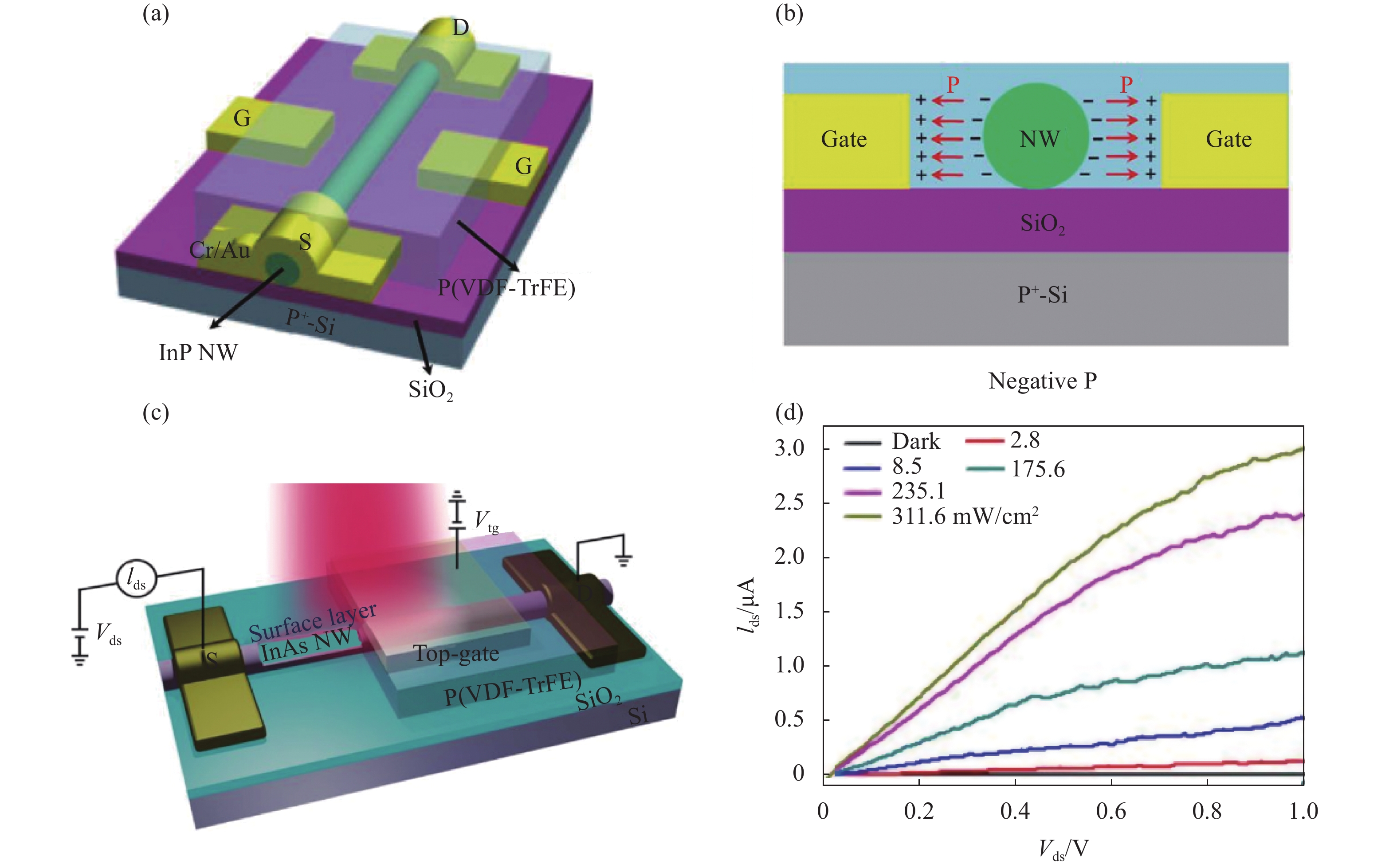
一方面,准一维纳米线具有为载流子提供了高速的导电通道、易实现大面积生长、制备成本低、表面积体积比大且载流子浓度易于调控等优点,是实现高性能光电探测的一种可行的结构体系;另一方面,纳米线在材料制备过程中容易引入杂质和缺陷诱导高浓度的背景载流子,使得基于纳米线制备的光电器件暗电流偏高。利用栅电极的电压对铁电材料极化调控形成局域电场抑制纳米线沟道材料的暗电流,从而提高探测器件的灵敏度是一种可行办法。2016年,Hu等人[15]率先提出利用铁电聚合物P(VDF-TrFE)薄膜作为介质层,采用侧栅结构制备磷化铟(InP)和硫化镉(CdS)单根纳米线晶体管。聚偏氟乙烯(PVDF)常见的晶型主要有四种,分别为α、β、γ和δ相。理想的β相PVDF分子呈反式结构,极性最强,电偶极矩最大。但β相在室温下不是非常稳定,因此通过在PVDF中引入一定数量的三氟乙烯(TrFE)能够形成新的有机铁电聚合物P(VDF-TrFE)。P(VDF-TrFE)可以在较低温度下获取,并直接通过旋涂法整合在低维材料上,利用界面上非易失性的静电场对沟道材料进行电子或者空穴的有效掺杂。该器件能够通过侧栅电极极化铁电材料产生超强局域电场有效耗尽纳米线本征载流子降低暗电流,显著提高探测器的信噪比。InP纳米线侧栅结构器件如图1(a)所示,该器件根据铁电材料的极化情况分为三种工作状态:无极化状态、负向极化状态、正向极化状态。图1(b)为负向极化状态下的工作原理图,此时P(VDF-TrFE)薄膜的极化方向由纳米线指向侧栅电极,n型InP中的电子在局域电场作用下被耗尽使得导带能级上升,沟道电流低至皮安量级处于耗尽态;而当P(VDF-TrFE)薄膜为正向极化状态时,极化方向与上述情况相反,是由侧栅电极指向纳米线,这时导带能级下降。因此器件的暗电流在负向极化状态下被有效抑制,得益于这种独特的结构,InP纳米线光电器件在830 nm的入射光照射下获得了高达4.2×10⁵的光电导增益,响应率为2.8×10⁵ AW−1,探测率为9.1×10¹⁵ Jones,比传统商用Si器件的探测率高出两个数量级以上。受限于材料本身的带隙,以上铁电材料调控单根InP、CdS纳米线的光电器件探测波长分别为可见-近红外(500~1200 nm)和紫外-可见(350~700 nm)。砷化铟(InAs)纳米线作为一种典型的直接带隙Ⅲ-Ⅴ族半导体材料,具有超高的载流子迁移率和窄禁带宽度(~0.35 eV),已被广泛应用于红外光电探测研究领域[16-17]。与侧栅结构类似,2019年,Zhang等人[18]制备了铁电聚合物P(VDF-TrFE)薄膜作为顶栅介质层、InAs纳米线为沟道材料的晶体管光电器件(图1(c))。通过施加大小为45 V、方向不同的电压脉冲使得P (VDF-TrFE)薄膜处于三种不同的极化状态:初始状态、极化向上(Pup)和极化向下(Pdown)。当铁电材料极化向下时,纳米线表面围绕着正电荷,在这些正电荷的作用下,InAs纳米线表面的缺陷态能够俘获大量的电子。这些被缺陷态束缚住的电子形成局域静电场,使得纳米线内部的载流子被耗尽,表现出极低的暗电流。此时在450 nm光照下,光生电子不会被表面氧化层的束缚能级捕获,而是贡献到光电流中。同时,通过这种电子预填充表面缺陷态的方式,能够消除表面态引起的电离散射效应,进一步提高纳米线核中的载流子迁移率和寿命。图1(d)所示为器件在波长为3.5 μm激光照射下的输出特性曲线,光生电流占主导,使得器件在红外波段有明显响应,而且光电流随光功率的增加而显著增加。因此InAs纳米线能够在铁电局域场的调控下实现截止波长边缘(~3.5 μm)处的高灵敏探测,在3.5 μm光照射下获得高达1.6×10⁴ AW−1的响应率,1.4×1012 Jones的探测率,5.7×103的增益。此外,中国科学院上海微系统与信息技术研究所Di等人[19]也利用铁电聚合物P(VDF-TrFE)薄膜作为侧栅介质层调控GeSn/Ge双层纳米线,该器件的暗电流和静态功耗同样被大幅降低,从而实现了长波长与低暗电流的光电探测。以上铁电材料调控纳米线的研究成果表明,铁电极化局域场能够显著提高纳米线光电探测器的性能,促进了低维纳米线材料在光电探测领域的发展。

图 1 铁电局域场增强纳米线光电探测器。(a)铁电材料调控单根InP纳米线侧栅器件结构示意图;(b)器件在负向极化状态的工作原理图[15];(c)铁电材料调控单根InAs纳米线顶栅器件结构示意图;(d)器件在不同功率密度的3.5 μm激光照射下的输出特性曲线[18]
Figure 1. Ferroelectric localized field-enhanced nanowire photodetectors. (a) Device structure schematic of ferroelectric side-gated single InP NW; (b) Working principle diagram of the device in the negative polarization state[15]; (c) Device structure schematic of ferroelectric top-gated single InAs NW; (d) Output characteristic curves of the device for 3.5 μm exciting light at different power densities[18]
-
二维材料是一类层内通过共价键而层间通过范德瓦尔斯力连接的层状材料,工艺上可以通过机械剥离法直接从体材料中获得薄层二维材料。二维材料中的邻近效应、量子限域效应、强电子相互作用使得其表现出区别于体材料的电学及光学特性[20]。过渡金属硫族化合物(TMDs)是二维材料中研究的最广泛的材料之一,其中二硫化钼(MoS2)因具有高载流子迁移率、带隙可调、稳定性好及可大面积制备等优点成为了研究热点[21-22]。MoS2与铁电材料的复合结构被多次报道,2015年,中国科学院上海技术物理研究所Wang等人[14]利用P(VDF-TrFE)调控MoS2光电器件,图2(a)为其器件结构图,9 nm的金属铝薄膜作为半透明顶栅,三层MoS2纳米片作为沟道导电材料。当顶栅施加一定大小和方向的电压时,P(VDF-TrFE)能够保持向上或者向下的极化方向,极化作用形成的局域电场能够显著调控沟道材料的载流子浓度。当极化方向向上时,该光电器件可获得极低暗电流,使光开关比达到三个量级,响应率最高为2570 AW−1,探测率为2.2×10¹² Jones,截止波长从850 nm拓展到1550 nm (图2(b))。此外,铁电材料在极化反转过程中由于电压放大效应表现出负电容效应,已有多项工作基于二维材料与铁电材料的结构实现了负电容效应,使得亚阈值摆幅低于60 mV/dec。作为光电器件,调控其亚阈值摆幅能够增强光生电压对沟道电流的调控,从而提升器件的光探测灵敏度。2020年,Tu等人[23]通过图2(c)所示结构,利用氧化铪基铁电薄膜材料调控MoS2纳米片得到负电容光电场效应晶体管,该器件基于氧化铪基铁电薄膜的负电容效应能够实现极低的亚阈值摆幅。该器件随入射光功率变化下的转移特性曲线如图2(d)所示,转移特性随光功率的增大发生左移,阈值电压变化量增加。这是由于随着光功率变大,光生电子空穴对增加,而被捕获的空穴也随之增加。该器件将低维材料中普遍存在的Photogating效应与铁电材料的负电容效应相结合,有效地抑制暗电流,使得该器件能够在室温下实现高灵敏光电探测。以上方法均具有普适性,对其他二维材料的器件结构设计和性能优化具有参考价值。
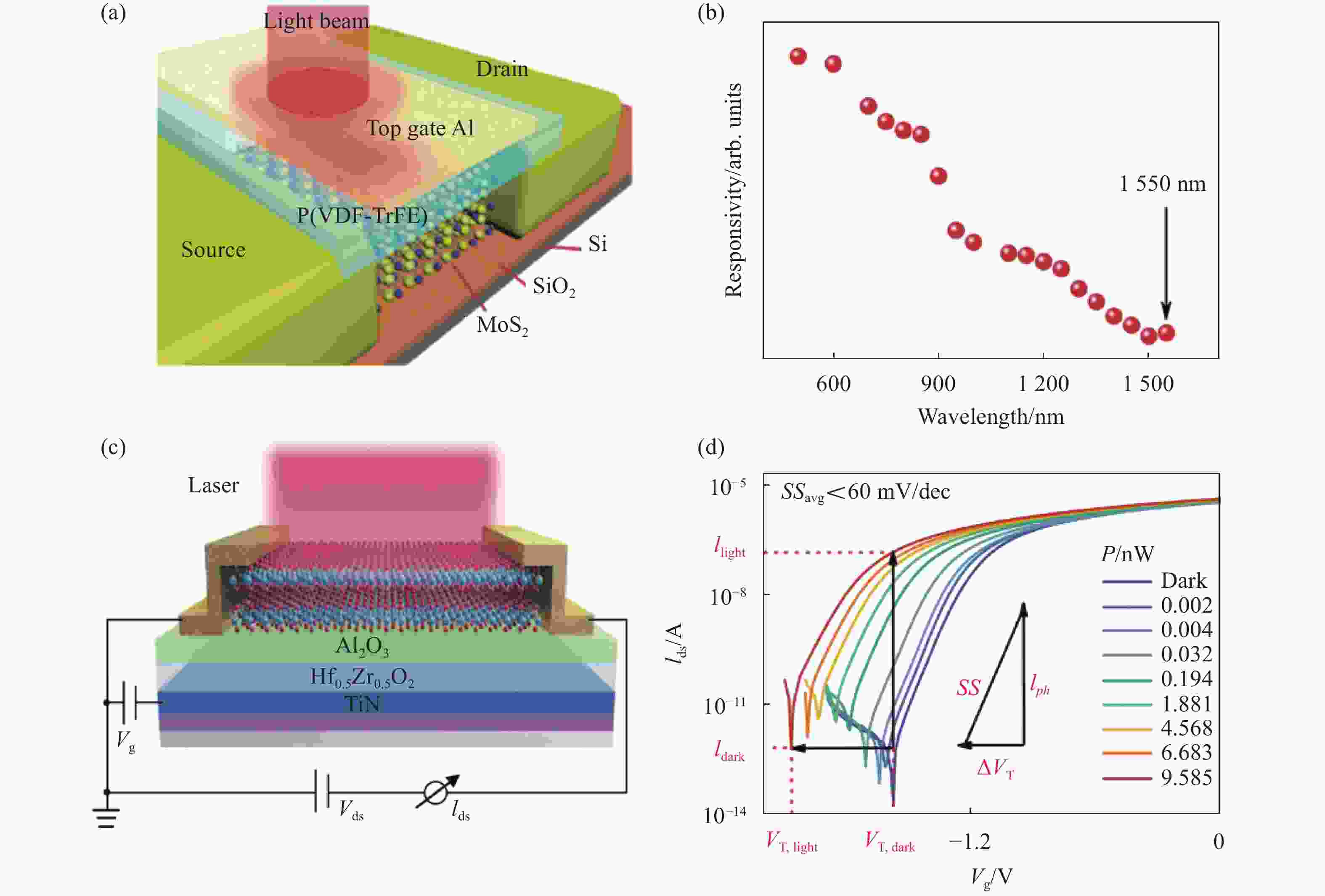
图 2 铁电局域场增强MoS2光电探测器。(a)铁电材料调控MoS2顶栅器件结构示意图;(b)不同光波长下的响应率[14];(c)铁电材料调控MoS2负电容场效应晶体管结构及测试电路示意图;(d)不同入射光功率下的转移特性曲线[23]
Figure 2. Ferroelectric localized field-enhanced MoS2 photodetector. (a) Schematic diagram of MoS2 top-gate device structure tuned by ferroelectric material; (b) Photoresponsivity under different wavelength[14]; (c) Schematic diagram of structure and test circuit of MoS2 negative capacitance field effect transistor tuned by ferroelectric material; (d) Transfer characteristic curves under different incident light powers[23]
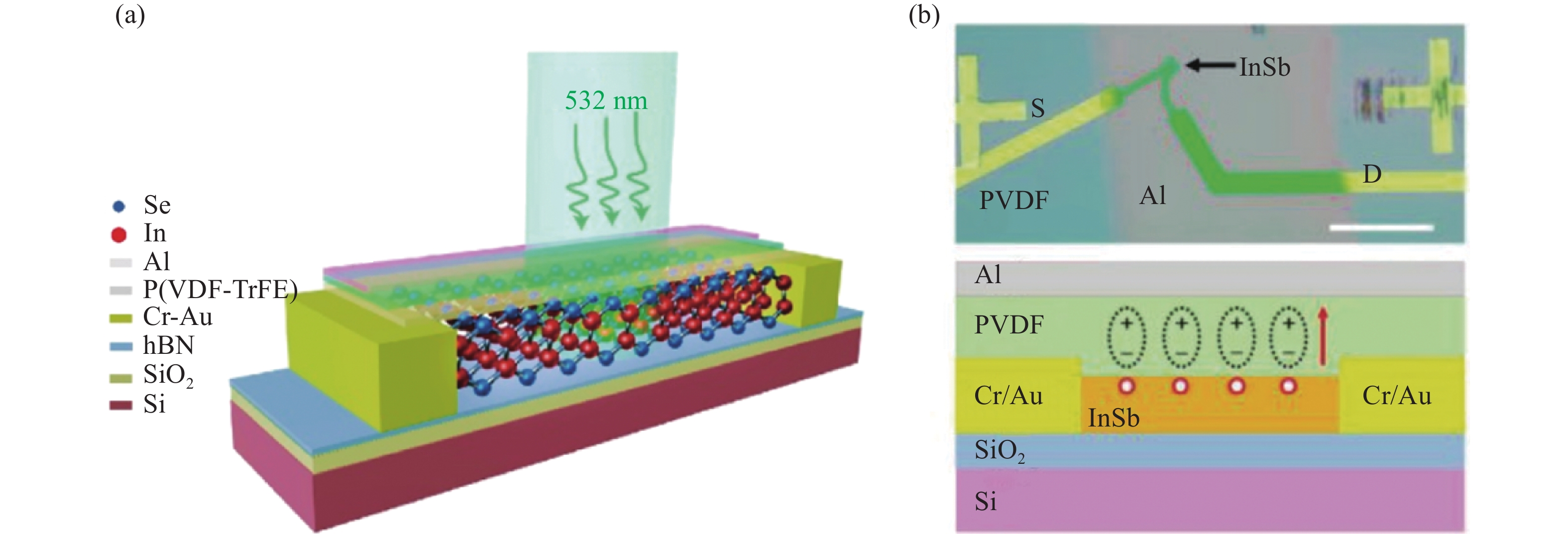
多样化的二维材料具有丰富的物理性质,研究人员们也同样利用铁电局域场来提升其他二维材料的光电性能。硒化铟(InSe)是一种典型的Ⅲ-Ⅵ族二维半导体材料,因其载流子迁移率高,带隙适中且可调,展现出极大的光电探测潜力[24-25]。2020年,Qin等人[26]将P(VDF-TrFE)作为顶栅介质层,h-BN作为衬底改善界面,制备了InSe光电晶体管(如图3(a)所示)。通过调控铁电材料的极化状态向上,使得InSe沟道材料在顶栅铁电介质层产生的超强局域场作用下,载流子保持在完全耗尽的状态,暗电流成功地被抑制至~10−14 A,开关比高达八个量级以上,光响应率为14250 AW−1,探测率为1.63×10¹³ Jones。比起极化向上状态时光生电流占沟道电流主导作用,未极化和向下极化状态时,光激发载流子和热离子/隧穿载流子均贡献了沟道电流。文中也对传统栅控和铁电栅控的InSe光电探测器进行了比较分析:(1)介质层的介电常数比传统的SiO2和Al2O3大10左右;(2)与背栅场效应晶体管结构相比,该结构中的InSe被h-BN和P(VDF-TrFE)包裹,可以有效改善材料的降解和散射,高质量的界面也能够有效防止SiO2中的电荷杂质扩散;(3)铁电介质层极化向上状态的剩余极化电场可以完全耗尽由缺陷/陷阱态引起的载流子浓度,所以暗电流能够被有效抑制。另一种特殊的半导体材料锑化铟(InSb)在Ⅲ-Ⅴ族化合物中是电子有效质量最小、电子迁移率最高、带隙最小的材料,因此InSb能够在低功耗和高速电子学、红外探测中展现出巨大的应用潜能。但传统的InSb红外探测器受暗电流大的限制,通常需要在低温下工作。当InSb尺寸减小至纳米结构时,声子散射被抑制,暗电流减小,工作温度也可提高[27]。但样品表面的缺陷依然极大地影响了InSb的光电性能,为了改进并提高其光电探测灵敏度,需要外加栅压调控器件的工作状态。Zhang等人[28]研究了铁电材料调控的二维InSb红外光电探测器(如图3(b)所示),利用铁电薄膜P(VDF-TrFE)钝化纳米片表面,而铁电材料的极化电场也提供了所需的栅压。使得该器件展现了宽光谱(637 nm~4.3 μm)探测的能力,暗电流低至4 nA,响应速度从秒提高至毫秒。
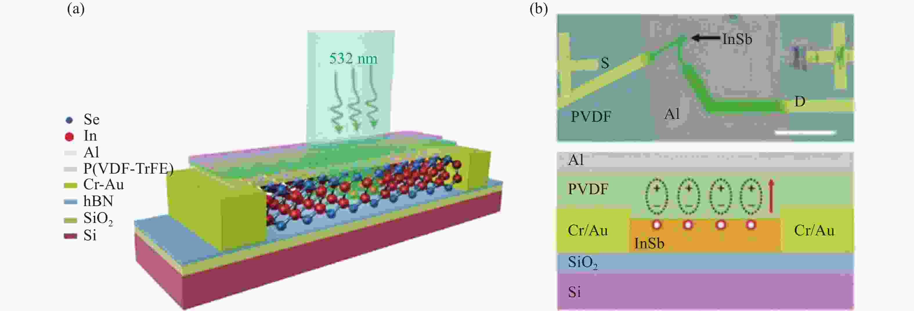
图 3 铁电局域场增强二维材料光电探测器。(a)铁电材料调控InSe光电晶体管结构示意图[26];(b) 铁电材料调控InSb光电晶体管结构示意图[28]
Figure 3. Ferroelectric localized field-enhanced two-dimensional material photodetectors. (a) Structure schematic of ferroelectric material tuned InSe phototransistor[26]; (b) Structure schematic of ferroelectric material tuned InSb phototransistor[28]
以上介绍了铁电材料利用剩余极化产生的局域电场调控不同二维材料的研究成果。此外,铁电材料自身的热释电特性也被用来提升二维材料的光电特性。2017年,U. Sassi等人[29]将石墨烯转移到铌酸锂(LiNbO3)上,然后通过沉积浮动栅的工艺得到基于石墨烯的中波红外探测器(如图4(a)所示)。在红外信号的辐照下,LiNbO3温度的变化产生热释电荷使得图4(b)中电容C3电荷量发生改变,在电容器C2上产生顶栅电压,这种器件结构中浮栅的放大设计使电阻温度系数高达900%/K,增益高达200,温度分辨率为15 μK,在室温下实现了12 μm中红外探测。2020年,Wang等人[30]利用铁电材料P(VDF-TrFE)的热释电特性和二维半导体材料MoS2的光电导特性,基于铁电局域场调控的二维半导体场效应晶体管结构,开发了具有超宽光谱(375 nm~10 μm)响应的光电探测器。器件结构如图4(c)所示,为了对器件进行热隔离处理,铁电材料作为栅介质层的MoS2器件制备在超薄的聚酰亚胺衬底上。在紫外至近红外波段,铁电局域场增强MoS2的光电导效应,实现对可见光目标的单像素成像;在中长波红外波段,信号响应来源于铁电材料的热释电特性,然后通过二维材料读出并放大,光电流开关比超过三个量级。而Zheng等人[31]同样在PMN-PT(001)铁电单晶衬底上外延生长高质量的二维Bi2O2Se薄膜,实现了2D铁电场效应晶体管(如图4(d)所示)。该器件在可见光和红外光共同照射下表现出偏振相关的光响应。这些研究成果进一步表明铁电局域场增强促进了基于二维材料制备的红外宽光谱探测器件的研制。

图 4 铁电材料热释电效应调控二维材料光电探测器。(a)石墨烯热释电辐射热计示意图;(b)石墨烯热释电辐射热计工作原理图[29];(c) P(VDF-TrFE)/MoS2场效应晶体管结构[30];(d) Bi2O2Se/PMN-PT铁电场效应晶体管结构示意图[31]
Figure 4. Modulation of two-dimensional material photodetectors by pyroelectric effect of ferroelectric materials. (a) Schematic diagram of graphene pyroelectric bolometer; (b) Working principle diagram of graphene pyroelectric bolometer[29]; (c) P(VDF-TrFE)/MoS2 field effect transistor structure[30]; (d) Structure schematic of Bi2O2Se/PMN-PT ferroelectric field effect transistor[31]
-
PN结是电子和光电器件基本的元器件,二维材料因敏感的界面特性极易被外部调控成为制备PN结的原材料之一。利用二维材料制备的PN结器件按材料可分为同质结和异质结,同质结是指利用静电掺杂、元素掺杂、表面化学修饰和厚度调控等方法在同一种材料中形成的结;而异质结是将两种掺杂类型不同的材料通过工艺手段直接堆叠或者外延生长等方法形成的结。下面主要介绍铁电材料调控二维材料制备的同质结和异质结及其作用机理。
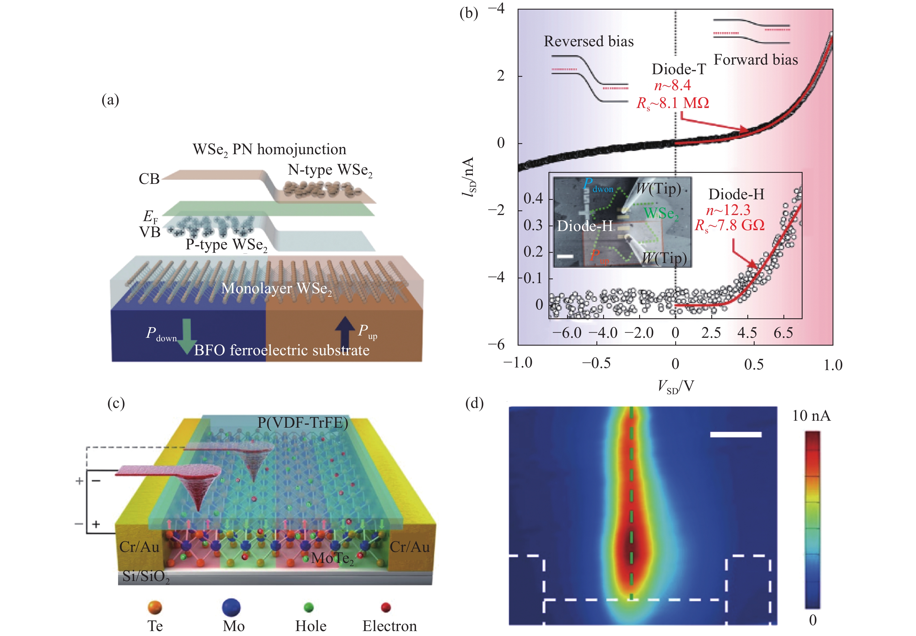
制备二维材料PN结的方法中,静电掺杂是通过在同一材料的不同区域配置方向相反的电压引起不同掺杂类型,该方法需要不间断供压,能耗大。而元素掺杂、表面化学修饰和厚度调控等方法均是不可逆的。铁电材料局域场调控基于二维材料制备的同质结能够通过外部电压调节极化方向获得不同类型的结,且具有非易失性。例如,Chen等人[32]将单层二硒化钨(WSe2)转移到BiFeO3衬底上,利用压电力显微镜(PFM)将铁电衬底左右两块区域分别极化且极化方向相反(如图5(a)所示)。极化方向向下区域处的WSe2材料中被注入电子,使得费米能级上移;极化方向向上区域处的WSe2材料中被注入空穴,使得费米能级下移。因此,在铁电畴壁位置处的WSe2形成了面内PN结,图5(b)所示的输出特性曲线证实了这一点。沿用类似的方法,Wu等人[33]制备了铁电材料P(VDF-TrFE)作为栅介质层的MoTe2晶体管,如图5(c)所示,利用原子力显微镜上带电的针尖对P(VDF-TrFE)产生极化作用形成局域电场,进一步掺杂与之接触的MoTe2纳米片。通过调控不同区域铁电材料的极化方向可以对MoTe2进行P型掺杂或者N型掺杂来得到面内PN结,光电流mapping测试证实了峰值电流存在结区处(图5(d))。随后,该研究团队进一步采用裂栅电极结构制备MoTe2晶体管[34]。通过裂栅电极所加电压不同极化P(VDF-TrFE)得到高性能面内PN结器件,整流比高达5×105。在探测光信号时展现了优异性能,光电转化效率为2.5%,探测波长可拓展至短波红外(1350 nm)。文献中也提到,这种结构具有普适性,可以应用到其他双极性层状材料上制备高质量面内PN结。
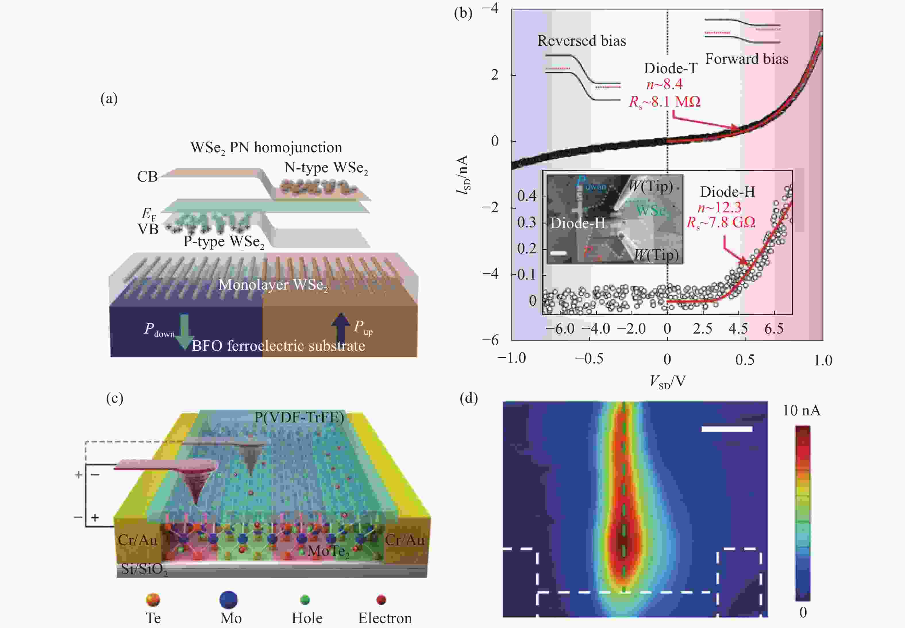
图 5 铁电局域场增强二维材料同质结器件。(a) BiFeO3调控的WSe2面内pn结示意图;(b)器件的输出特性[32];(c) P(VDF-TrFE)调控的MoTe2面内pn结示意图;(d)器件的光电流mapping图[33]
Figure 5. Ferroelectric localized field-enhanced two-dimensional material homojunction devices. (a) Schematic diagram of BiFeO3 ferroelectric tuned WSe2 in-plane pn junction; (b) Output characteristics of the device[32]; (c) Schematic diagram of P(VDF-TrFE) ferroelectric tuned MoTe2 in-plane pn junction; (d) Photocurrent mapping of the device[33]
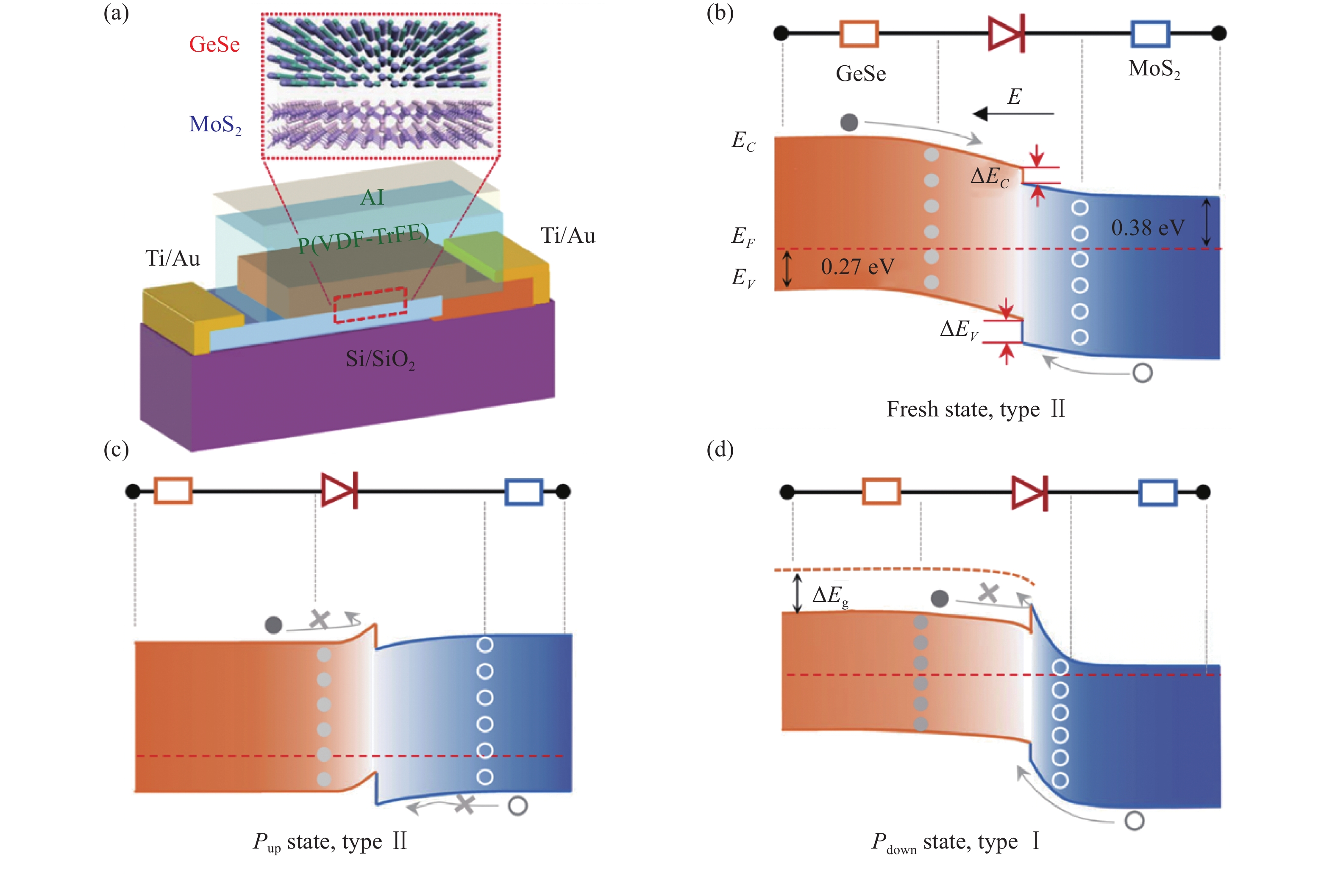
在低维材料众多的研究成果中,异质结占据不可或缺的地位。传统的异质结器件在工艺上需要苛刻的条件避免界面污染,而晶格常数的匹配限制了异质结的材料选择。低维材料层与层之间是靠范德瓦尔斯力结合,在制备异质结器件时能够实现无键结合,不必考虑晶格常数匹配和材料加工工艺的问题。精确控制不同的二维材料构筑异质结构,可以实现全新的电子、光学、机械性能。2021年,Chen等人[35]在GeSe/MoS2异质结晶体管结构中引入铁电局域场,器件结构如图6(a)所示。其中GeSe为各向异性材料,具有电学各向异性和光学线性二向色性,能够实现偏振探测。将P(VDF-TrFE)旋涂在GeSe/MoS2异质结上作为顶栅介质层,GeSe/MoS2的能带结构在铁电极化场作用下,异质结的能带结构从Ⅱ类转化为Ⅰ类。当P(VDF-TrFE)为未极化状态时,GeSe与MoS2形成Ⅱ类异质结(如图6(b)所示),有利于光生载流子的分离;当P(VDF-TrFE)极化向上时,GeSe材料中积累空穴,MoS2中电子耗尽,导致GeSe的能带向上弯曲,少数载流子的漂移电流受限,反向电流低于未极化状态(如图6(b)所示);当P(VDF-TrFE)极化向下时,反向电流在小偏压下被抑制,大偏压下显著增加,能带结构变成Ⅰ类(如图6(d)所示)。由于铁电偶极子的能带工程,该器件在近红外区域也很敏感。此外,GeSe的各向异性使得器件在可见至近红外波段范围内能够实现高灵敏的偏振探测,在铁电局域场的辅助下,器件的偏振探测比也大大提高了,该成果为能带工程构建多功能器件提供了新思路。
图 6 铁电局域场增强二维范德华异质结器件[35]。(a) 铁电调控异质结GeSe/MoS2器件结构示意图;(b)~(d) 铁电材料处于不同极化状态时异质结的能带结构示意图
Figure 6. Ferroelectric localized field-enhanced two-dimensional van der Waals heterojunction devices[35]. (a) Device structure schematic of ferroelectric tuned GeSe/MoS2 heterojunction; (b)-(d) Schematic diagram of the energy band structure of the heterojunction corresponding to the different ferroelectric polarization states
-
文中简要介绍了铁电局域场增强低维材料光电探测器的一些最新研究成果。这些光电器件主要依赖于铁电材料极化形成的局域强电场作用调控低维材料中的载流子浓度,从而显著提高其光电探测性能。传统的背栅静电场调控器件需要不间断施加电压,具有易失性,导致工作条件复杂,功耗大。铁电材料的剩余极化可以重复反转,因此铁电局域场的引入不仅能够极大地提高和拓展低维材料的光电特性和功能性,而且满足了低功耗的需求,为获得新一代高性能光电探测器奠定基础。然而,目前铁电局域场增强低维材料光电探测器的研究大多数集中在带隙较宽的材料,探测波长在可见至近红外区间,对探测中远红外波段的材料性能提升有待提高。主要原因是窄带隙材料本征载流子浓度过高,很难有效提取光生载流子。因此,考虑结合铁电局域场与其他结构共同作用降低中长波探测材料的暗电流,有效提取光生电流是一种重要的途径。此外,将大面积生长的二维材料与铁电薄膜结合实现大面积图形化加工制备阵列式光电子器件同样具有很大的发展潜力。
Research progress on ferroelectric localized field-enhanced low-dimensional material-based photodetectors (invited)
-
摘要: 光电探测器在通讯、环境、健康和国防等日常生活及国家安全等领域中应用广泛。随着时代的发展,对光电探测器在灵敏度、响应速度及波长范围等方面的性能要求与日俱增。低维材料独特的电学及光电特性使其在光电子器件领域具有重要的应用前景。为了充分利用低维材料的优势,克服其暗电流大、吸收率低的不足,研究人员提出将铁电材料与低维材料结合,利用铁电材料的剩余极化作用形成强局域场调控载流子浓度以提高低维材料的光电探测能力。文中总结了近年来铁电局域场增强低维材料光电探测器的研究成果,介绍了铁电材料对一维纳米线、二维材料以及低维结型器件的调控和性能提升方面的相关研究。最后,对铁电局域场增强低维材料光电探测器的发展趋势进行了简要的总结和展望。Abstract: Photodetectors are widely used in daily life and national security, including communication, the environment, health and national defense. With the development of time, the performance requirements of photodetectors in terms of sensitivity, response speed and wavelength range have been increasing. The unique electrical and optoelectronic properties of low-dimensional materials make them an essential application prospect in the field of optoelectronic devices. To make full use of the advantages of low-dimensional materials and overcome the shortcomings of high dark current and low absorption rate, researchers have combined ferroelectric materials with low-dimensional materials and used the remnant polarization of ferroelectric materials to form a strong localized field to modulate carriers, which improves the photodetection capability of low-dimensional materials. Recent research results of ferroelectric localized field-enhanced low-dimensional material-based photodetectors are summarized in this paper. Meanwhile, related research on the modulation and performance enhancement of ferroelectric materials in one-dimensional nanowires, two-dimensional materials and junction devices was introduced. Finally, the development trend of ferroelectric localized field-enhanced low-dimensional material-based photodetectors was briefly summarized and proposed.
-
Key words:
- ferroelectric localized field /
- low-dimensional materials /
- photodetector
-
图 1 铁电局域场增强纳米线光电探测器。(a)铁电材料调控单根InP纳米线侧栅器件结构示意图;(b)器件在负向极化状态的工作原理图[15];(c)铁电材料调控单根InAs纳米线顶栅器件结构示意图;(d)器件在不同功率密度的3.5 μm激光照射下的输出特性曲线[18]
Figure 1. Ferroelectric localized field-enhanced nanowire photodetectors. (a) Device structure schematic of ferroelectric side-gated single InP NW; (b) Working principle diagram of the device in the negative polarization state[15]; (c) Device structure schematic of ferroelectric top-gated single InAs NW; (d) Output characteristic curves of the device for 3.5 μm exciting light at different power densities[18]
图 2 铁电局域场增强MoS2光电探测器。(a)铁电材料调控MoS2顶栅器件结构示意图;(b)不同光波长下的响应率[14];(c)铁电材料调控MoS2负电容场效应晶体管结构及测试电路示意图;(d)不同入射光功率下的转移特性曲线[23]
Figure 2. Ferroelectric localized field-enhanced MoS2 photodetector. (a) Schematic diagram of MoS2 top-gate device structure tuned by ferroelectric material; (b) Photoresponsivity under different wavelength[14]; (c) Schematic diagram of structure and test circuit of MoS2 negative capacitance field effect transistor tuned by ferroelectric material; (d) Transfer characteristic curves under different incident light powers[23]
图 3 铁电局域场增强二维材料光电探测器。(a)铁电材料调控InSe光电晶体管结构示意图[26];(b) 铁电材料调控InSb光电晶体管结构示意图[28]
Figure 3. Ferroelectric localized field-enhanced two-dimensional material photodetectors. (a) Structure schematic of ferroelectric material tuned InSe phototransistor[26]; (b) Structure schematic of ferroelectric material tuned InSb phototransistor[28]
图 4 铁电材料热释电效应调控二维材料光电探测器。(a)石墨烯热释电辐射热计示意图;(b)石墨烯热释电辐射热计工作原理图[29];(c) P(VDF-TrFE)/MoS2场效应晶体管结构[30];(d) Bi2O2Se/PMN-PT铁电场效应晶体管结构示意图[31]
Figure 4. Modulation of two-dimensional material photodetectors by pyroelectric effect of ferroelectric materials. (a) Schematic diagram of graphene pyroelectric bolometer; (b) Working principle diagram of graphene pyroelectric bolometer[29]; (c) P(VDF-TrFE)/MoS2 field effect transistor structure[30]; (d) Structure schematic of Bi2O2Se/PMN-PT ferroelectric field effect transistor[31]
图 5 铁电局域场增强二维材料同质结器件。(a) BiFeO3调控的WSe2面内pn结示意图;(b)器件的输出特性[32];(c) P(VDF-TrFE)调控的MoTe2面内pn结示意图;(d)器件的光电流mapping图[33]
Figure 5. Ferroelectric localized field-enhanced two-dimensional material homojunction devices. (a) Schematic diagram of BiFeO3 ferroelectric tuned WSe2 in-plane pn junction; (b) Output characteristics of the device[32]; (c) Schematic diagram of P(VDF-TrFE) ferroelectric tuned MoTe2 in-plane pn junction; (d) Photocurrent mapping of the device[33]
图 6 铁电局域场增强二维范德华异质结器件[35]。(a) 铁电调控异质结GeSe/MoS2器件结构示意图;(b)~(d) 铁电材料处于不同极化状态时异质结的能带结构示意图
Figure 6. Ferroelectric localized field-enhanced two-dimensional van der Waals heterojunction devices[35]. (a) Device structure schematic of ferroelectric tuned GeSe/MoS2 heterojunction; (b)-(d) Schematic diagram of the energy band structure of the heterojunction corresponding to the different ferroelectric polarization states
-
[1] Jiang W, Zheng T, Wu B, et al. A versatile photodetector assisted by photovoltaic and bolometric effects [J]. Light: Science & Applications, 2020, 9(1): 160-160. [2] Long M, Wang P, Fang H, et al. Progress, challenges, and opportunities for 2D material based photodetectors [J]. Advanced Functional Materials, 2019, 29(19): 1803807. doi: 10.1002/adfm.201803807 [3] Wang J, Han J, Chen X, et al. Design strategies for two-dimensional material photodetectors to enhance device performance [J]. InfoMat, 2019, 1(1): 33-53. doi: 10.1002/inf2.12004 [4] Fang J, Zhou Z, Xiao M, et al. Recent advances in low-dimensional semiconductor nanomaterials and their applications in high-performance photodetectors [J]. InfoMat, 2020, 2(2): 291-317. doi: 10.1002/inf2.12067 [5] Rezaei M, Bianconi S, Lauhon L J, et al. A new approach to designing high-sensitivity low-dimensional photodetectors [J]. Nano Letters, 2021, 21(23): 9838-9844. doi: 10.1021/acs.nanolett.1c03665 [6] Zhang M, Liu X, Duan X, et al. Schottky-contacted WSe2 hot-electron photodetectors with fast response and high sensitivity [J]. ACS Photonics, 2022, 9(1): 132-137. doi: 10.1021/acsphotonics.1c01256 [7] Xu Y, Liu C, Guo C, et al. High performance near infrared photodetector based on in-plane black phosphorus p-n homojunction [J]. Nano Energy, 2020, 70(1): 104518. [8] Chen Y, Ma W, Tan C, et al. Broadband Bi2O2Se photodetectors from infrared to terahertz [J]. Advanced Functional Materials, 2021, 31(14): 2009554. doi: 10.1002/adfm.202009554 [9] Liu D, Liu F, Liu Y, et al. Schottky-contacted high-performance GaSb nanowires photodetectors enabled by lead-free all-inorganic perovskites decoration [J]. Small, 2022, 18(16): 2200415. doi: 10.1002/smll.202200415 [10] Yin Y, Guo Y, Liu D, et al. Substrate-free chemical vapor deposition of large-scale III-V nanowires for high-performance transistors and broad-spectrum photodetectors [J]. Advanced Optical Materials, 2022, 10(6): 2102291. doi: 10.1002/adom.202102291 [11] Sun J, Han M, Peng M, et al. Stoichiometric effect on electrical and near-infrared photodetection properties of full-composition-range GaAs1-xSbx nanowires [J]. Nano Research, 2021, 14(11): 3961-3968. doi: 10.1007/s12274-021-3321-3 [12] Sun J, Peng M, Zhang Y, et al. Ultrahigh hole mobility of Sn-catalyzed GaSb nanowires for high speed infrared photodetectors [J]. Nano Letters, 2019, 19(9): 5920-5929. doi: 10.1021/acs.nanolett.9b01503 [13] Wang J, Fang H, Wang X, et al. Recent progress on localized field enhanced two-dimensional material photodetectors from ultraviolet-visible to infrared [J]. Small, 2017, 13(35): 1700894. doi: 10.1002/smll.201700894 [14] Wang X, Wang P, Wang J, et al. Ultrasensitive and broadband MoS2 photodetector driven by ferroelectrics [J]. Advanced Materials, 2015, 27(42): 6575-6581. doi: 10.1002/adma.201503340 [15] Zheng D, Wang J, Hu W, et al. When nanowires meet ultrahigh ferroelectric field-high-performance full-depleted nanowire photodetectors [J]. Nano Letters, 2016, 16(4): 2548-2555. doi: 10.1021/acs.nanolett.6b00104 [16] Miao J, Hu W, Guo N, et al. High-responsivity graphene/InAs nanowire heterojunction near-infrared photodetectors with distinct photocurrent on/off ratios [J]. Small, 2015, 11(8): 936-942. doi: 10.1002/smll.201402312 [17] Fang H, Hu W, Wang P, et al. Visible light-assisted high-performance mid-infrared photodetectors based on single InAs nanowire [J]. Nano Letters, 2016, 16(10): 6416-6424. doi: 10.1021/acs.nanolett.6b02860 [18] Zhang X, Huang H, Yao X, et al. Ultrasensitive mid-wavelength infrared photodetection based on a single InAs nanowire [J]. ACS Nano, 2019, 13(3): 3492-3499. doi: 10.1021/acsnano.8b09649 [19] Yang Y, Wang X, Wang C, et al. Ferroelectric enhanced performance of a GeSn/Ge dual-nanowire photodetector [J]. Nano Letters, 2020, 20(5): 3872-3879. doi: 10.1021/acs.nanolett.0c01039 [20] Huang C, Li Y, Wang N, et al. Progress in research into 2D graphdiyne-based materials [J]. Chemical Reviews, 2018, 118(16): 7744-7803. doi: 10.1021/acs.chemrev.8b00288 [21] Manzeli S, Ovchinnikov D, Pasquier D, et al. 2D transition metal dichalcogenides [J]. Nature Reviews Materials, 2017, 2(8): 17033. doi: 10.1038/natrevmats.2017.33 [22] Wang Q H, Kalantar-Zadeh K, Kis A, et al. Electronics and optoelectronics of two-dimensional transition metal dichalcogenides [J]. Nature Nanotechnology, 2012, 7(11): 699-712. doi: 10.1038/nnano.2012.193 [23] Tu L, Cao R, Wang X, et al. Ultrasensitive negative capacitance phototransistors [J]. Nature Communications, 2020, 11(1): 101. doi: 10.1038/s41467-019-13769-z [24] Sucharitakul S, Goble N J, Kumar U R, et al. Intrinsic electron mobility exceeding 103 cm2/(V s) in multilayer InSe FETs [J]. Nano Letters, 2015, 15(6): 3815-3819. doi: 10.1021/acs.nanolett.5b00493 [25] Wu F, Xia H, Sun H, et al. AsP/InSe Van der Waals tunneling heterojunctions with ultrahigh reverse rectification ratio and high photosensitivity [J]. Advanced Functional Materials, 2019, 29(12): 1900314. doi: 10.1002/adfm.201900314 [26] Liu L, Wu L, Wang A, et al. Ferroelectric-gated InSe photodetectors with high on/off ratios and photoresponsivity [J]. Nano Letters, 2020, 20(9): 6666-6673. doi: 10.1021/acs.nanolett.0c02448 [27] Bockelmann U, Bastard G. Phonon scattering and energy relaxation in two-, one-, and zero-dimensional electron gases [J]. Physical Review B, 1990, 42(14): 8947-8951. doi: 10.1103/PhysRevB.42.8947 [28] Zhang S, Jiao H, Wang X, et al. Highly sensitive InSb nanosheets infrared photodetector passivated by ferroelectric polymer [J]. Advanced Functional Materials, 2020, 30(51): 2006156. doi: 10.1002/adfm.202006156 [29] Sassi U, Parret R, Nanot S, et al. Graphene-based mid-infrared room-temperature pyroelectric bolometers with ultrahigh temperature coefficient of resistance [J]. Nature Communications, 2017, 8(1): 14311. doi: 10.1038/ncomms14311 [30] Wang X, Shen H, Chen Y, et al. Multimechanism synergistic photodetectors with ultrabroad spectrum response from 375 nm to 10 μm [J]. Advanced Science, 2019, 6(15): 1901050. doi: 10.1002/advs.201901050 [31] Yan J-M, Ying J-S, Yan M-Y, et al. Optoelectronic coincidence detection with two-dimensional Bi2O2Se ferroelectric field-effect transistors [J]. Advanced Functional Materials, 2021, 31(40): 2103982. doi: 10.1002/adfm.202103982 [32] Chen J-W, Lo S-T, Ho S-C, et al. A gate-free monolayer WSe2 pn diode [J]. Nature Communications, 2018, 9(1): 3147. doi: 10.1038/s41467-018-05599-2 [33] Wu G, Tian B, Liu L, et al. Programmable transition metal dichalcogenide homojunctions controlled by nonvolatile ferroelectric domains [J]. Nature Electronics, 2020, 3(1): 43-50. doi: 10.1038/s41928-019-0350-y [34] Wu G, Wang X, Chen Y, et al. MoTe2 p-n homojunctions defined by ferroelectric polarization [J]. Advanced Materials, 2020, 32(16): 1907937. doi: 10.1002/adma.201907937 [35] Chen Y, Wang X, Huang L, et al. Ferroelectric-tuned van der Waals heterojunction with band alignment evolution [J]. Nature Communications, 2021, 12(1): 4030. doi: 10.1038/s41467-021-24296-1 -

 点击查看大图
计量
- 文章访问数: 485
- HTML全文浏览量: 144
- PDF下载量: 158
- 被引次数: 0

