


 下载:
下载:


-
随着以智能汽车快速充电、特高压智能电网以及新能源储能逆变等需求为引领的第三代半导体技术的发展,由氮化镓、单晶碳化硅为主要代表的新型材料逐渐从理论层面走向实际应用,目前直径300 mm或更大尺寸单晶碳化硅材料的制备已经成为现实。随着材料尺寸的增加和成熟度的提高,单晶碳化硅不仅在半导体领域有着绝佳的应用前景,由于其高热导率、大弹性模量及高温条件下工作稳定等特点,在传统成像光学及强激光领域同样是极具潜力的光学材料[1-4]。同时,单晶碳化硅由于其很好的材料均匀性,相比较于现在已成熟应用的RB-SiC,并不需要通过表面镀制CVD或者PVD改性层就可以获得满足于大部分光学需求的表面质量,简化了工艺流程,提高了可靠性。基于单晶碳化硅材料的高性能光学元件以及光学系统具有较大的应用前景,但同时由于单镜碳化硅接近于金刚石的硬度,其加工难度具有极高挑战性,除了如何通过光学加工获得较高的面形精度(RMS或PV)外,单晶碳化硅这种硬脆材料表面粗糙度的研究同样是高精度制造的基础。
粗糙度是衡量光学元件表面质量的重要指标之一,对于传统成像光学应用,粗糙度Ra值一般要求小于3 nm,而对于比如强激光或极紫外等特殊应用,粗糙度Ra一般要求优于1 nm或更小。目前已广泛应用于航空航天领域的RB-SiC,其莫氏硬度在9以上,由于其两相表面且硬度高难加工的特点,目前主流的加工手段,在SiC阶段仅能获得约7 nm的表面粗糙度,通过表面镀制Si改性层进行再次抛光,从而达到3 nm及以下的表面粗糙度[5-8]。单晶碳化硅的莫氏硬度相较于RB-SiC更高,在9.5左右,但因其不存在两相结构,理论上可以直接获得3 nm甚至优于1 nm的表面粗糙度而不需要通过表面镀制改性层。但硬度越高,加工工艺流程越多,不仅会极大地影响加工效率,且前道工艺加工留下的高频误差会影响最终粗糙度的结果。上述难点为单晶碳化硅获得高表面粗糙度带来了挑战,严重制约了单晶碳化硅材料在光学元件领域的应用。
目前,国内外众多学者对单晶碳化硅的加工方法进行了研究。如德国Wacker的WenSki通过对转速与压力关系的研究,利用双面抛光工艺对300 mm晶圆的边缘过抛问题进行了修正[9];美国II-VI光学的Everson及韩国ECC的Lee G S等人通过利用KOH、胶体二氧化硅溶液等具有腐蚀性的抛光液来实现单晶碳化硅这种超硬材料的低粗糙度获取[10-11];国内李娟、姜守振等人通过对磨料、压力等不同工艺参数的研究,在单晶碳化硅上实现了2.5 nm的表面粗糙度[12];大连理工大学的郭东明等利用掺杂Al2O3改进抛光液对单晶碳化硅表面粗糙度进行了研究[13];清华大学的潘国顺等利用CMP原理进行单晶碳化硅超光滑表面的获取[14-15]。
虽然国内外相关单位开展了大量单晶碳化硅表面质量方面的研究,但主要集中在抛光压力及磨料等工艺参数上或基于双面抛光设备工艺制造超光滑表面,制作工艺流程相对较短且主要基于晶圆半导体方向的应用。在传统光学加工中,比如微晶玻璃、RB-SiC等常见的光学材料加工,往往利用计算机控制小磨头(CCOS)技术采用子口径修形的方式加工平面、球面、非球面乃至自由曲面[16-21],中国科学院长春光学精密机械与物理研究所的曾雪锋和国防科技大学的李奇等人关于中频对光学表面误差及光学系统像质的影响做了较详尽的研究,也通过引入PSD曲线及熵增理论等方式讨论了中频误差的评价及抑制方法[22-23],但对高频尤其是粗糙度频段的研究较少,通过对单晶碳化硅材料的前期实验可知,如果不仅追求表面粗糙度,同时要求较高的面形精度时,光学加工的工艺链路会延长,超硬材料的长时间多轮加工所残留的误差严重阻碍高表面粗糙的实现,同时单一Ra值表面粗糙度评价指标相对于不同工艺下粗糙度的表征也不够完整。
文中提出了一种基于PSD评价及熵增理论的伪随机轨迹加工改善单晶碳化硅表面粗糙度的方法。通过对粗糙度常用采样数据的分析,确定了PSD计算评价方法;利用热力学中常用的熵增原理,从理论上分析了确定性抛光轨迹和伪随机轨迹对粗糙度尺度下累计误差影响的区别。该方法丰富了粗糙度的评价维度,验证了特定采样区间下的PSD曲线作为粗糙度评价手段的有效性,同时论证了伪随机轨迹相较于确定性轨迹在单晶碳化硅材料上的优势,证明了文中所述方法的实用性。突破了超硬材料在长时间固定轨迹加工下导致中高频累积从而影响最终粗糙度的瓶颈技术。
-
功率谱密度 (Power spectral density, PSD)作为评价不同频段下误差分布的指标最早在1997年ISO公布的ISO-10110-8中被提出。作为不同频段下误差分布评价指标,无论是从普通面形误差计算得到低频、中频信息,还是高频段信息都可以适用,比SlopeRMS应用更广泛。PSD曲线常常绘制为关于空间频率(mm−1或μm−1)下的面形误差分量(μm2或mm2)的连续曲线,如若在所测的数据误差中某个空间频率成分较大,在PSD曲线上可观察到线条的凸起或尖锐形状,相反的,PSD曲线越平滑。在实际工作中,PSD曲线越平滑,则表征光学元件表面误差分布越无序化,而周期性明显的误差分布对成像质量有较大影响。文中采用二维离散傅里叶变换来计算PSD,最后将PSD曲线绘制为常见的一维形式。对于常见的白光干涉仪采样数据可知,作图区间定为1/15 ~ 1/400 μm−1较合理。二维离散傅里叶变换公式为:
$$ {{X}}_{{{k}}_{1},{{k}}_{2}}={\sum }_{{{n}}_{1}=0}^{{{N}}_{1}-1}\left({{\omega }}_{{{N}}_{1}}^{{{k}}_{1}{{n}}_{1}}\sum\nolimits _{{{n}}_{2}=0}^{{{N}}_{2}-1}\left({{\omega }}_{{{N}}_{2}}^{{{k}}_{2}{{n}}_{2}}{\cdot {x}}_{{{n}}_{1},{{n}}_{2}}\right)\right) $$ (1) 式中:xn1,n2为二维N1×N2离散数据在下标(n1,n2)处的数据值;ωN1= exp(−i2π/Nl),kl = 0, 1, ··· , Nl – 1,其中l = 1, 2。
-
光学元件的抛光主要采用计算机控制下小工具加工(Computer controlled optical surfacing, CCOS)的方式,加工后往往会产生被称作为“刀痕”的表面规律性误差结构。在对单晶碳化硅的研究过程中发现,与传统光学材料类似,相较于理论去除函数,实际去除函数由于压力分布不均匀或其他抛光参数的扰动会产生较严重的变形;而由于硬度高去除效率较低的原因,单晶碳化硅的加工周期相对较长,需要经过更多轮的加工迭代,上述效应会更趋于明显。
CCOS加工中常见的加工轨迹如图1所示,分别为光栅轨迹方式及螺旋线轨迹方式。这两种极具规律性的轨迹规划方式通过反复迭代加工会不断放大实际去除函数与理论去除函数的偏差,并将偏差中的高频信息残留在光学元件表面,对粗糙度产生周期性的误差影响。

图 1 确定性轨迹规划。(a)光栅轨迹;(b)螺旋线轨迹
Figure 1. Deterministic tool path. (a) Grating tool path; (b) Helix tool path
综上所述,确定性的轨迹规划如光栅和螺旋线产生的确定性频段误差可以类比于热力学系统中相对有无的有序性和无序性讨论:有序性高的系统中,各组成状态的一致性较弱;无序性高的系统中,相反地,各组成部分状态的一致性高。那么,基于热力学系统中的熵增原理,光栅和螺旋线轨迹产生的粗糙度频段误差可以利用非确定性的,可根据驻留点分布变化的轨迹所改善。
根据热力学中熵的定义可知,系统中不确定性可以表述为概率密度和随机变量之间的关系,对于离散随机变量Y = {y1, y2, ···yn}, R = {r1, r2, ···rn}为其对应的概率密度,那么,随机变量的不确定性的测度被定义为熵:
$$ S(R)=-\sum\nolimits_{i=1}^{n}\left(r_{i} \ln r_{i}\right) $$ (2) 式中:
${\displaystyle\sum\nolimits }_{{i}=1}^{{n}}\left({{r}}_{{i}}\right)=1$ ri ≥ 0。如果当ri =0,rk=1(k ≠ i)时,熵有最小值S = 0;当任意ri = 1 / n 时,熵达到最大值S (R)= ln(n)。CCOS加工过程中,小工具经过的轨迹可以理解为信号过程,所以熵函数可以用来评价加工过程中轨迹的方向的不确定性。一般来讲,轨迹可能行进的方向越多,其熵值越大,那么加工过程的随机性就越强。因此,无论是通过改进步距还是改变进刀方向,光栅和螺旋线这类确定性轨迹规划,从熵的角度讲,都不如每次加工方向都可以随机变化的轨迹规划方式,可以推论,此类轨迹可以抑制粗糙度频段的误差。图2为生成的一种伪随机轨迹示意图。

图 2 一种伪随机轨迹示意图
Figure 2. Diagram of a pseudo-random tool path
-
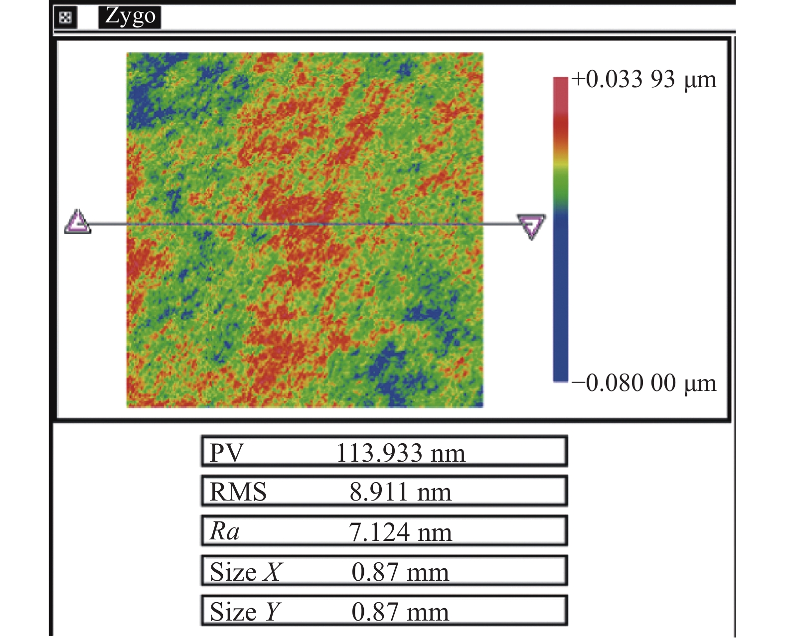
为了验证前述的分析,利用机器人抛光中心对两片6 in单晶碳化硅进行光学抛光。考虑到驻留时间仿真计算的一致性,排除边缘效应的影响,因此在模拟计算收敛时,只考虑中心4 in范围内子孔径区域。这两片单晶碳化硅前道工序为同批次双面研抛加工,因此初始粗糙度具有一致性,采用Zygo白光干涉仪在同一放大倍率下测量,结果如图3所示。

图 3 采用Zygo 9000白光干涉仪进行粗糙度测量
Figure 3. Roughness test by Zygo newview 9000 white-light interferometry
由图4可以看出,初始粗糙度Ra值约为7 nm。
分别采用伪随机轨迹与确定性轨迹进行光学加工,每种轨迹均进行10轮、每轮40 min的遍历抛光。对于确定性轨迹,以光栅轨迹为例,光栅驻留点间隔为1 mm,考虑到实际加工过程中,也不存在同一个驻留轨迹多次重复加工的情况,而往往会变换轨迹的起始位置从而达到刀痕错位效果,因此该实验中每轮轨迹起始点间隔错位0.1 mm。

图 4 加工前白光干涉仪测量结果
Figure 4. Measurement results of white-light interferometry before machining
如图5所示,在用光栅轨迹抛光过后,白光干涉仪所测数据计算得到Ra值为1.207 nm,对该数据计算PSD曲线,如图6所示。图6的横坐标表示空间频率,单位为μm−1,而高度误差分布图的PSD曲线的纵坐标单位与高度误差分布图的纵坐标单位为同一量纲,这里单位为nm。可以明显看到在该PSD曲线横坐标0.01 μm−1附近出现了尖峰,这与前述分析一致,同确定性轨迹抛光的加工方法强相关。
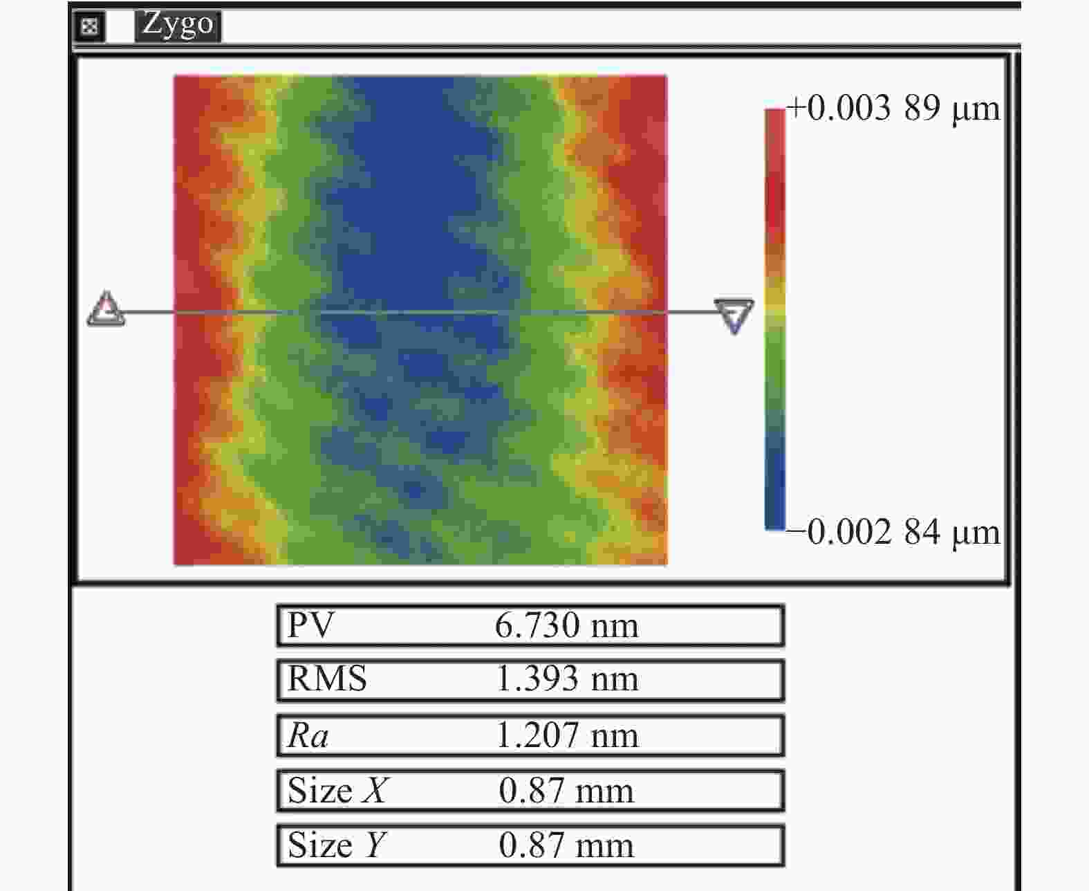
图 5 光栅轨迹加工后白光干涉仪测量结果
Figure 5. Measurement result of white-light interferometry after grating trajectory processing

图 6 利用光栅轨迹所测数据计算得到PSD曲线
Figure 6. PSD curve calculated by data of grating trajectory
图7所示为采用伪随机轨迹加工过后的白光干涉仪所测数据,Ra值为1.045 nm,计算其PSD曲线如图8所示。由此可以看出,曲线较平滑,没有明显的尖峰存在。

图 7 伪随机轨迹加工后白光干涉仪测量结果
Figure 7. Roughness result after processing with pseudo-random trajectory

图 8 利用伪随机轨迹所测数据计算得到PSD曲线
Figure 8. PSD curve calculated by data of pseudo-random trajectory
由上述实验分析可以得到,初始表面经过确定性轨迹和伪随机轨迹抛光后,虽然二者Ra值相近,但PSD曲线可以明显表征出二者区别,确定性轨迹具有尖峰型特征存在,而伪随机轨迹的PSD曲线则更为平滑,没有明显的尖峰。验证了PSD曲线评价粗糙度和伪随机轨迹加工的有效性的同时表明伪随机轨迹加工获得的表面质量更高。
-
文中提出了一种基于PSD评价及熵增理论的伪随机轨迹加工改善单晶碳化硅表面粗糙度的方法。通过对粗糙度常用采样数据的分析,确定了PSD计算评价方法;利用热力学中常用的熵增原理,从理论上分析了确定性抛光轨迹和伪随机轨迹对粗糙度尺度下的累计误差影响。通过对6 in单晶碳化硅进行多轮抛光,分析实验结果得出:在约Ra=7 nm相同初始粗糙度情况下,确定性轨迹与伪随机轨迹均得到了Ra约1 nm的粗糙度值,但PSD曲线可以明显看出确定性轨迹出现了明显的尖峰,而伪随机轨迹则更为平滑。验证了特定采样区间下的PSD曲线作为粗糙度评价手段的有效性,同时论证了伪随机轨迹相较于确定性轨迹在单晶碳化硅材料上的优势,证明了文中所述方法的实用性。
Study on surface roughness of monocrystalline silicon carbide based on PSD evaluation and pseudo-random tool path
-
摘要: 随着新能源、特高压需求爆发,以单晶碳化硅为代表的第三代半导体技术近几年得到了飞速发展,大口径单晶碳化硅材料制备已经成为现实,相比于目前已成熟应用的RB-SiC材料,单晶碳化硅不需要通过CVD或PVD改性就可以获得1 nm甚至更优的表面粗糙度,在光学元件领域的应用具有广阔前景,但同时加工难度高是亟待解决的问题。为了解决单晶碳化硅材料在光学加工过程中的粗糙度问题,提出了一种基于PSD评价及熵增理论的伪随机轨迹加工改善粗糙度的方法。相较于传统单一的Ra值评价方法,通过引入PSD曲线丰富了粗糙度评价的维度;利用对熵增理论的分析,从理论上讨论了确定性抛光轨迹和伪随机轨迹对粗糙度尺度下累计误差影响的区别。通过对6 in (1 in=2.54 cm)单晶碳化硅进行多轮抛光实验,结果表明:在相同初始粗糙度情况下,确定性轨迹与伪随机轨迹虽均得到了Ra约1 nm的粗糙度值,但PSD曲线可以明显看出确定性轨迹出现了尖峰,而伪随机轨迹则更为平滑。验证了特定采样区间下的PSD曲线作为粗糙度评价手段的有效性,同时论证了伪随机轨迹相较于确定性轨迹在单晶碳化硅材料抛光上的优势。Abstract:
Objective As a novel material leading the third-generation semiconductor technology revolution, monocrystalline silicon carbide has a very excellent prospect in the application of semiconductor field. And because of its high thermal conductivity, high elastic modulus, and high temperature stability, it is a highly competitive material in traditional imaging optics, high-power laser optics and other fields. Under some circumstances, such as application scenarios as high-power laser optics or EUV optics, the surface roughness Ra needs to be less than 1 nm or even much lower. Obviously, such high-performance specifications necessitate much more precise optical manufacturing for these types of optical applications. In traditional optical manufacturing, the technology of CCOS (Computer Controlled Optical Surfacing) is a commonly utilized manufacturing procedure in the whole process of optical manufacturing. Although some researchers at home and abroad have conducted detailed investigations on the influence of CCOS processing on MSF (Middle Spatial Frequency) errors for optical surfaces, there is a lack of research on the influence of CCOS processing on HSF (High Spatial Frequency) errors for optical surfaces. The intensity of the HSF errors of optical surfaces directly determines the surface roughness. Therefore, it is necessary to find a proper solution to how to evaluate the HSF errors for optical surfaces and how to reduce the HSF errors, which determines the surface roughness, when the overall HSF errors and surface roughness don’t meet expectations. Methods PSD (Power Spectral Density) is the most commonly utilized indicator to evaluate the distribution of intensities of different frequencies for a certain signal. The sudden-peak form on a PSD curve indicates a sudden increase of the intensity of certain frequency band for the said signal, and at the same time, the peak form on a PSD curve will directly lead to the increase of the surface roughness. Inspired by the principle of the increase of entropy, experiments were conducted on two monocrystalline SiC flat surfaces with similar initial surface roughness distributions. One surface was processed with a pseudo-random tool path which was based on the Gilbert space-filling curve (Fig.2), while the other was processed with a conventional deterministic rasterized trajectory (Fig.1(a)). Finally, the surface roughness distributions and PSD curves of the two surfaces after the experiment were analyzed. Results and Discussions Through the comparison of the experiment of the two surfaces, it can be seen that both two monocrystalline SiC surfaces have an approximate initial roughness Ra=7 nm (Fig.4) and then get experimented with 10 sets of 40 minutes' polishing. And after the polishing process is completed for both surfaces, the PSD curve of the surface processed with a deterministic rasterized tool path contains a sudden peak nearby frequency domain 0.01 μm−1 (Fig.6), whereas the PSD curve of the surface processed with pseudo-random tool path appears to be much smoother (Fig.8). In the meantime, the test results show that the surface processed with the pseudo-random tool path has lower roughness, which in turn indicates that the surface quality is higher after processing with the pseudo-random tool path. Conclusions PSD is one of the most versatile indicators when it comes to signal analysis. And enlightened by law of the increase of entropy in thermodynamics, and all other things being equal, the deterministic rasterized tool path is simply replaced with a pseudo-random one. And the final testing results are significantly different. That is, when making use of CCOS technology to process monocrystalline SiC, the pseudo-random tool path can be utilized to reduce the relative intensity of HSF errors of a certain surface. And it proves that the pseudo-random tool path in the CCOS processing stage has a great inhibiting effect on the HSF errors of optical surfaces and therefore facilitates lower surface roughness and better surface quality. -
Key words:
- monocrystalline silicon carbide /
- pseudo-random tool path /
- roughness
-
图 1 确定性轨迹规划。(a)光栅轨迹;(b)螺旋线轨迹
Figure 1. Deterministic tool path. (a) Grating tool path; (b) Helix tool path
图 3 采用Zygo 9000白光干涉仪进行粗糙度测量
Figure 3. Roughness test by Zygo newview 9000 white-light interferometry
图 4 加工前白光干涉仪测量结果
Figure 4. Measurement results of white-light interferometry before machining
图 5 光栅轨迹加工后白光干涉仪测量结果
Figure 5. Measurement result of white-light interferometry after grating trajectory processing
图 7 伪随机轨迹加工后白光干涉仪测量结果
Figure 7. Roughness result after processing with pseudo-random trajectory
-
[1] Li Liting. Research progress of silicon carbide semiconductor materials and suggestions for its industrial development [J]. Xiamen Science & Technology, 2016(5): 1-11. (in Chinese) [2] Bi Keyun, Li Songfa. The development of wide band gap semiconductor device [J]. Journal of Caeit, 2016, 1(1): 6-10. (in Chinese) [3] Lebedev A A, Chelnokov V E. Wide-gap semiconductors for high-power electronics [J]. Semiconductors, 1999, 33(9): 999-1001. doi: 10.1134/1.1187823 [4] Lendenmann H, Bergman J P, Dahlquist F, et al. Degradation in SiC bipolar devices: Sources and consequences of electrically active dislocations in SiC [J]. Materials Science Forum, 2003, 433: 901-906. [5] Wang Xu. Evaluation of the RB-SiC mirror surface fabricated with the fixed abrasive technology [J]. Infrared and Laser Engineering, 2012, 41(9): 2074-2479. (in Chinese) [6] Li Zhuolin, Lee W B. Study on removal characteristic of silicon carbide surface in precision mechanical polishing [J]. Infrared and Laser Engineering, 2016, 45(2): 0220003. (in Chinese) doi: 10.3788/m0001820164502.220003 [7] Li Lingzhong, Wang Xiaokun, Qi Erhui, et al. Research status analysis of subsurface damage characterization and measurement technology of optical components (invited) [J]. Infrared and Laser Engineering, 2022, 51(12): 20220572. (in Chinese) doi: 10.3788/IRLA20220572 [8] Gao Shang, Li Tianrun, Lang Hongye, et al. Prediction for subsurface damage depth of silicon wafers in workpiece rotational grinding [J]. Optics and Precision Engineering, 2022, 30(17): 2077-2087. (in Chinese) doi: 10.37188/OPE.20223017.2077 [9] Wenski G, Altmann T, Winkler W, et al. Doubleside polishing—a technology mandatory for 300 mm wafer manufacturing [J]. Materials Science in Semiconductor Processing, 2002, 5(4-5): 375-380. [10] Everson W J, Snyder D, Heydemann V D. Polishing and surface characterization of SiC substrates[C]//Materials Science Forum, 2000. [11] Lee G S, Hwang H H, Son C H, et al. The effect of slurry composition and flatness on sub-surface damage and removal in chemical mechanical polishing of 6H-SiC [J]. Materials Science Forum, 2009, 615-617: 605. doi: 10.4028/www.scientific.net/MSF.615-617.605 [12] Jiang Shouzhen, Xu Xiangang, Li Juan, et al. Recent progress in SiC monocrystal growth and wafer machining [J]. Chinese Journal of Semiconductor, 2007, 28(5): 810-814. [13] Guo Dongming, Kang Renke, Su Jianxiu, et al. Future development on wafer planarization technology in ulsi fabrication [J]. Chinese Journal of Mechanical Engineering, 2003, 39(10): 100-105. [14] Pan G S, Gu Z H, Zhou Y, et al. Preparation of silane modified SiO2 abrasive particles and their Chemical Mechanical Polishing (CMP) performances [J]. Wear, 2011, 273(1): 100-104. doi: 10.1016/j.wear.2011.05.044 [15] Zhou Yan, Pan Guoshun, Shi Xiaolei, et al. Chemical Mechanical Planarization (cmp) of on-axis si-face sic wafer using catalyst nanoparticles in slurry [J]. Surface & Coatings Technology, 2021, 43: 42-47. [16] Song Chi. Fabrication of large aspherics using non-Newtonian fluid polishing tool [D]. Beijing: University of Chinese Academy of Sciences, 2017. (in Chinese) [17] Li H Y, David W, Yu G Y, et al. Modeling and validation of polishing tool influence functions for manufacturing segments for an extremely large telescope [J]. Appl Opt, 2013, 52(23): 5781-5787. [18] Li Mingze, Hou Xi, Zhao Wenchuan, et al. Current situation and development trend of aspheric optical surface defect detection technology (invited) [J]. Infrared and Laser Engineering, 2022, 51(9): 20220457. (in Chinese) doi: 10.3788/IRLA20220457 [19] Liang Zijian, Yang Yongying, Zhao Hongyang, et al. Advances in research and applications of optical aspheric surface metrology [J]. Chinese Optics, 2022, 15(2): 161-186. doi: 10.37188/CO.2021-0143 [20] Wang Yaru, Li Yingjie, Zou Lai, et al. Material removal and surface damage behavior of diamond grain for flexible scribing RB-SiC [J]. Optics and Precision Engineering, 2022, 30(14): 1704-1715. (in Chinese) doi: 10.37188/OPE.20223014.1704 [21] Ma Zhanlong, Wang Junlin. Ultra-precision optical fabrication technology [J]. Infrared and Laser Engineering, 2013, 42(6): 1485-1490. (in Chinese) [22] Zeng Xuefeng, Zhang Xuejun. Impact of mid-spatial frequency errors in optical manufacturing on modulation transfer function [J]. Laser & Optoelectronics Progress, 2015, 52(7): 232-237. (in Chinese) [23] Li Qi. Study on stability improvement and path optimization in numerical control small tool polishing for optical component [D]. Changsha: National University of Defense Technology, 2014. (in Chinese) -

 点击查看大图

计量
- 文章访问数: 133
- HTML全文浏览量: 56
- PDF下载量: 22
- 被引次数: 0


