


 下载:
下载:


-
铌酸锂薄膜光子集成技术在过去十年增长迅速,因其极具吸引力的材料特性,包括大的二阶非线性磁化率、大的电光系数、宽的光学透明窗口、高折射率等,目前已经用于实现包括调制器、微环谐振器、光子晶体腔、及参量振荡器等[1-5],并用于片上光学功能实现,如非线性频率变换器[6-7]、非线性量子光源[8-9]、激光器[10]、电光调制、光频梳光谱仪等[11-14]。然而由于光纤的模斑尺寸与铌酸锂薄膜纳米波导的模斑尺寸严重失配导致光纤与铌酸锂薄膜纳米波导耦合时存在较大的耦合损耗,导致器件的插入损耗较大,严重限制铌酸锂薄膜光子器件的实用化,因此增加片上光学模式尺寸非常重要,不仅可以降低器件插入损耗,还可提高波导与光纤耦合对准容差。
片上模斑转换器被广泛用于模场变换,实现波导模场的变换。2019年,He等人采用双倒锥刻蚀波导,实现与锥形光纤模场匹配,耦合损耗1.7 dB/面[15]。2020年,Hu等人采用标准半导体工艺制造的端面耦合器,与模场直径约为3.2 μm的超高数值孔径光纤(UHNAF)耦合时,TE/TM光在1550 nm处的每面光纤芯片耦合损耗分别为0.54 dB/0.59 dB[16]。2021年,Pan等人采用双锥波导和SU8波导组合的边耦合器实现耦合损耗0.5 dB[17]。
现有研究虽然都提高了耦合效率,但都是与锥形光纤或者细径光纤的耦合,无法实现与单模光纤的高效耦合,并且对于实际应用来说,聚合物波导的温度稳定性又差,无法满足实际应用。文中采用三维有限差分传播法针对单模光纤高效耦合的模斑转换器进行仿真,结果表明,该结构可实现铌酸锂薄膜波导与单模光纤82.2%~89.0%的耦合效率,该设计可为铌酸锂薄膜光子器件工程化应用提供理论依据和仿真指导,有助于推动铌酸锂薄膜光子器件实用化发展进程。
-
铌酸锂薄膜波导采用典型的LNOI脊型结构,如图1所示,由硅基底、二氧化硅层(SiO2)和铌酸锂(LN)薄膜脊波导构成,通常LN薄膜典型厚度为600 µm,脊高度0.25 µm,其满足单模条件的模式面积比较小,约1 µm。典型单模保偏光纤的模场直径一般大于6 µm,导致光纤与波导之间存在显著的模式失配,导致较大的耦合损耗。

图 1 铌酸锂薄膜脊波导结构示意图
Figure 1. Schematic diagram of lithium niobate film ridge waveguide structure
为了实现铌酸锂薄膜波导与光纤的高效光耦合,采用在铌酸锂薄膜波导端面集成模斑转换器实现模式和能量的传递与转换。文中采用模斑转换器由SiO2、SiON锥形结构以及双层LN锥形结构组成,其结构如图2所示,其中双层LN锥形结构、SiON锥形结构用于光耦合与绝热模式转换,其中SiO2波导(Ⅰ)将用于定义与光纤耦合端面上的光模式,模式变换区包括SiON锥形、双层铌酸锂锥形结构,分为三个部分:SiON锥形线性变换区域(Ⅱ)、LN平板锥形区(Ⅲ)、以及LN脊型和平板构成的锥形区(Ⅳ),最后为LN脊波导区(Ⅴ)。

图 2 模斑转换器结构示意图
Figure 2. Structural diagram of spot size converter
-
三维有限光束差分传输算法可用于计算波导的本征模式及光束在波导中的传输情况[18-24]。在光纤和波导中,电磁波中的电场(磁场)满足Helmholtz方程:
$$ \frac{{{\partial ^2}\phi }}{{{\partial ^2}x}} + \frac{{{\partial ^2}\phi }}{{{\partial ^2}y}} + \frac{{{\partial ^2}\phi }}{{{\partial ^2}z}} + k{(x,y,z)^2}\phi = 0 $$ (1) 考虑到光轴主要沿Z轴传输,作近轴和慢变化近似,则
$$ \phi (x,y,z) = u(x,y,z){{\rm{e}}^{i\bar kz}} $$ (2) 式中:$ {{u}}(x,y,z) $为光波导中的传输场;$ \bar k = {k_0}\bar n $,表示$ \phi (x,y,z) $的平均相位变化,为参考波数;$ \bar n $为参考折射率,将公式(2)代入公式(1),得到:
$$ \frac{{{\partial ^2}u}}{{\partial {z^2}}} + 2i\bar k\frac{{\partial u}}{{\partial z}} + \frac{{{\partial ^2}u}}{{\partial {x^2}}} + \frac{{{\partial ^2}u}}{{\partial {y^2}}} + ({k^2} - {\bar k^2})u = 0 $$ (3) 作慢变化近似,即忽略$ \dfrac{{{\partial ^2}u}}{{\partial {z^2}}} $,则
$$ \frac{{\partial u}}{{\partial z}} = \frac{i}{{2\bar k}}\Bigg[\Bigg(\frac{{{\partial ^2}u}}{{\partial {x^2}}} + \frac{{{\partial ^2}u}}{{\partial {y^2}}} + ({k^2} - {\bar k^2})\Bigg]u $$ (4) 对公式(4)实行差分,得到:
$$ \frac{{u_i^{n + 1} - u_i^n}}{{\Delta z}} = \frac{i}{{2\bar k}}\left[ {\frac{{{\delta ^2}}}{{\Delta {x^2}}} + {k^2}({x_i},{z_{n + 1/2}}) - {{\bar k}^2}} \right]\frac{{u_i^{n + 1} + u_i^n}}{2} $$ (5) 式中:$ u_{\text{i}}^{\text{n}} $为第n个纵向平面上第i个格点处的电磁场分布;$ \Delta z $和$ \Delta {{x}} $为纵向平面之间的间隔和横向格点之间的间隔;$ {\delta ^2} $为标准二阶差分因子,$ {\delta ^2}{u_i} = ({u_{i + 1}} + {u_{i - 1}} - 2{u_i}) $,$ {z_{n + 1/2}} = {z_n} + \Delta z/2 $,根据公式(5)可求出波导传输方向任意位置处的电磁场分布。
对于波导与光纤之间的模式耦合效率可表示为:
$$ \eta = {\eta _{\text{1}}}{\eta _{\text{2}}}{\eta _{\text{3}}} $$ (6) 式中:耦合效率$ {\eta }_{1} $为耦合端面上氧化硅波导与单模光纤的耦合效率,由氧化硅波导与光纤中的电场重叠积分以及模式有效折射率所决定,公式表示为:
$$ {\eta _{\text{1}}} = \frac{{{{\left| {\displaystyle\iint {U_{fb}^ * \cdot {U_{WG}}{\rm{d}}x{\rm{d}}y}} \right|}^2}}}{{\displaystyle\iint {{{\left| {{U_{fb}}} \right|}^2}{\rm{d}}x{\rm{d}}y \cdot \displaystyle\iint {{{\left| {{U_{WG}}} \right|}^2}{\rm{d}}x{\rm{d}}y}}}} $$ (7) 耦合效率$ {\eta }_{2} $和$ {\eta }_{3} $分别表示从SiO2波导耦合端面传输到SiON波导模式转换效率和从SiON波导端面经双层LN锥形结构传输到LN脊型波导的模式转换效率。为了提高这俩部分耦合效率需要采用绝热模式传输,要求波导壁的局部扩展必须慢于最低阶模的衍射,即锥形波导的宽度变化尽可能缓慢,因此设计时需要在波导长度与模式转换效率之间进行权衡,在保持较高的模式转换效率的前提下尽可能缩短波导长度。
-
铌酸锂脊波导的单模工作条件受脊波导高度和宽度共同作用影响,随着波导高度增加,可实现基模工作的波导宽度越来越窄。文中选择脊高为0.25 µm,工作波长选取1550 nm,研究了不同脊波导宽度对铌酸锂薄膜波导内模式有效折射率的影响,其结果如图3所示。其中TE0、TE1、TE2、TE3分别为横电波的基模、一阶模、二阶模和三阶模,TM0、TM1为横磁波的基模、一阶模。从结果可以看出,单模工作条件内波导最大宽度为1 µm,为了提高结构的耦合效率,选择LN脊波导宽度为1 µm,此时,铌酸锂脊波导的基横模TE0分布如图4所示。
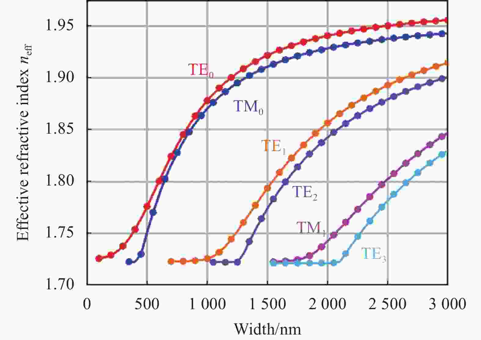
图 3 波导模式随脊波导宽度的变化
Figure 3. Variation of waveguide mode with ridge waveguide width

图 4 LN脊波导的基横模(TE0)分布
Figure 4. TE0 distribution of LN ridge waveguide
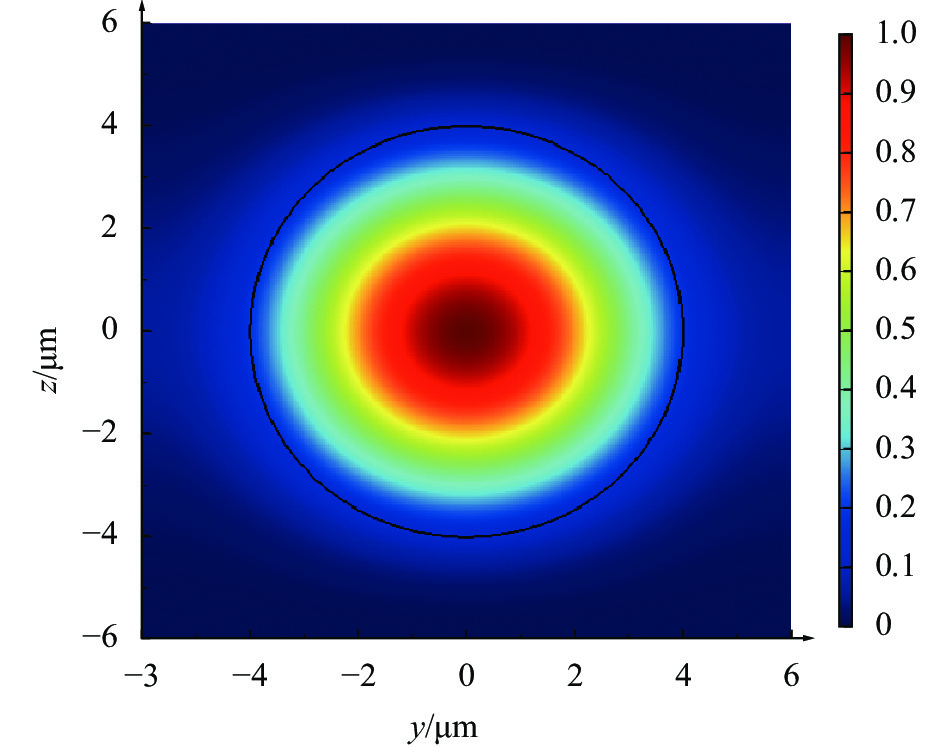
单模光纤采用标准的单模光纤,其参数选择如下:数值孔径0.14,芯径8.2 µm;包层直径125 µm,其模场分布如图5所示。从图中可以看出,其模场尺寸比铌酸锂脊波导的模场尺寸大很多。

图 5 单模光纤的模场分布
Figure 5. Mode field distribution of single-mode fiber
-
1) SiO2波导(I区)设计
SiO2波导用于实现与单模光纤的高效耦合,为了保证器件在1.55 µm波长处能够单模传输,SiO2波导需满足单模工作条件。综合目前SiO2波导工艺制备条件,文中选取常用的折射率差为0.75%的氧化硅波导,SiO2波导单模工作条件下不同的波导高度(H1)和宽度(W1)如图6(a)所示。考虑与光纤圆形光斑耦合匹配,SiO2波导的截面尺寸单模条件最优值选择6 µm×6 µm正方形波导结构,该条件下的SiO2波导x-y端面TE0模场分布如图6(b)所示,通过对二者模式进行重叠积分,可以得到SiO2波导与单模光纤的耦合效率$ {\eta }_{1} $为93%。

图 6 SiO2波导单模条件下波导参数和波导尺寸为 6 µm×6 µm时x-y端面TE0模场分布
Figure 6. Waveguide parameters of SiO2 waveguide under single mode condition and x-y cross sectional TE0 mode field distribution of SiO2 waveguide with 6 µm×6 µm waveguide size
2) SiON锥形波导设计(Ⅱ区)
SiON锥形波导主要决定从氧化硅波导耦合端面传输到SiON波导模式转换效率$ {\eta }_{2} $,包括耦合效率和传输效率两部分。为了实现高效绝热模式传输,SiON锥形波导宽端采用单模波导结构设计。SiON波导由SiON波导芯层和SiO2包层(n=1.456)构成,作为SiO2波导和LN脊波导的过渡波导设计,其单模模场尺寸应选取为二者模场的中间值,因此文中选取SiON波导的单模模场尺寸在2.5 µm×2.5 µm~3.5 µm×3.5 µm之间,来优化选择SiON波导芯层折射率。图7(a)为仿真得到的单模条件下最大波导模场宽度W2 (宽度和高度相同)与芯层折射率、波导宽度W2 (高度)之间的关系曲线。从结果可以看出,SiON波导芯层折射率选择1.48~1.51,对应波导宽度W2 (高度)在3.5~2.5 µm之间,可满足SiON波导模场设计。图7(b)给出了SiON波导芯层折射率为1.50,波导宽度(高度)为2.8 µm条件下的SiON波导x-y端面基横模TE0模场分布如图7(b)所示。

图 7 SiON波导单模条件及x~y端面TE0 模场分布
Figure 7. Single mode condition and x-y cross sectional TE0 mode field distribution of SiON waveguide
确定了SiON锥形波导宽端设计后,为了提高SiON锥形波导的转换效率,需要优化SiON锥形波导尖端宽度W3和锥形长度L1。以SiO2波导作为输入,SiON宽度波导作为输出,模拟仿真了SiON锥形波导尖端宽度W3取为=0.1 µm、0.2 µm、0.3 µm、0.4 µm的情况下锥形波导长度L1对转换效率的影响,如图8所示。由图8可知,耦合效率随着W3增加而减小,随L1增加而增大,当L1>250 µm且W3≤0.3 µm时,耦合效率可达到93%以上,当L1=300 µm,W3=0.1 µm时,转换效率可达97.2%。过渡区满足绝热模传输且长度较小时,其传输损耗可忽略不计,结合工艺实现考虑,L1可以在250~350 µm内变化,W3可以在0.2~0.3 µm内变化。

图 8 不同SiON锥形波导尖端宽度W1下锥形波导长度L1与转换效率关系曲线
Figure 8. Relation curve between taper waveguide length L1 and conversion efficiency under different SiON taper waveguide tip width W1
3)双层铌酸锂锥形区设计
双层铌酸锂锥形区包括LN平板锥形区(Ⅲ)、LN脊型和平板构成的锥形区(Ⅳ)。其中平板锥形区(Ⅲ)高度与LN脊波导区平板高度一致均为0.35 µm。首先对LN平板区波导宽端宽度W5进行了仿真,结果显示当平板宽端宽度W4>1.5 µm时,无法实现横向限制,转换效率低于50%,此外脊波导的平板区宽度一般为≥4 µm,为避免Ⅳ区平板宽度变化过大,因此LN平板锥形区宽端宽度不宜过小,可在0.8~1.5 µm内变化。
以SiON波导模式为入射光场,设定锥形区足够长(L2>500 µm),模拟了W4分别为0.8、1.0、1.2、1.4、1.5 µm情况下,锥形尖端宽度W5和LN平板锥形区的转换效率之间关系曲线如图9(a)所示。从图中可以看出平板锥形宽端宽度W5下对转换效率影响较小,锥形尖端宽度W5对转换效率影响较大,需要控制在0.15 µm以内,以实现>95%的转换效率,这是由于LN与SiON折射率存在差异,LN锥形尖端宽度直接关系着LN平板锥形区输出模场分布,对与SiON波导耦合效率影响较大。
在此基础上进一步对平板锥形区长度L2进行了设计。令W5=0.1 µm,仿真了W4=0.8、1.0、1.2、1.4和1.5 µm情况下,平板锥形区长度L2与LN平板锥形区对平板锥形区的转换效率的影响,如图9(b)所示。从图中可以看出,转换效率随着L2的增大而增大,随着W5的减小而增大,当L2>200 µm且W5<1.4 µm时,转换效率都可达>95%以上。这是由于锥形区长度足够长,可以有效减少锥形区模式泄露而产生的模式准换损耗,因此L2与可以在200~300 µm内变化,W4可以在0.1~0.15 µm内变化,W5可以在0.8~1.4 µm内变化,可实现LN平板锥形区转换效率在96%以上,当W4=0.1 µm,L2=200 µm时,可实现转换效率为98.5%。

图 9 W5 和L2对III区转换效率的影响
Figure 9. The influence of W5 and L2 on the conversion efficiency in Zone III
对于LN脊型和平板构成的锥形区(Ⅳ),其宽端宽度和各层高度与LN脊型波导参数一致。为了提高该区转换效率,以LN平板锥形区宽端波导模式作为入射光场,LN脊型波导模式作为出射光场,模拟了Ⅳ区不同锥形尖端宽度W6条件下,Ⅳ区锥形长度L3与Ⅳ区的转换效率之间关系曲线如图10所示。从图中可以看出转换效率随着L3增加,先增加后趋于稳定,随着W6的减小而增加,当L3>20 µm且W6≤0.4 µm时,转换效率在98%以上。综合套刻工艺实现和传输效率考虑,Ⅳ区脊型锥宽与平板尖端锥宽相差不能过近,因此,L3可以在40~100 µm内变化,W6可以在0.1~0.3 µm内变化,可实现脊型和平板构成的锥形区的转换效率在99%以上。

图 10 不同锥形尖端宽度W6条件下,IV区锥形长度L3与转换效率之间关系曲线
Figure 10. Relation curve between taper length L3 and conversion efficiency in Zone IV under different taper tip width W6
4)模斑转换器传输光场分析
通过上述理论计算与仿真优化,结合工艺实现性,得到模斑转换器的结构、传输光场(YZ面)以及不同位置截面图的光模式分布如图11(a)~(c)所示。Ⅰ区为光纤制合端面上 SiO2波导中的光模式分布(参见图11(c)中①所示),与单模光纤耦合效率为93%。Ⅱ区SiON锥形结构中的光模式分布(参见图11(c)中②所示),光模式逐渐从SiO2波导中向SION波导(参见图11(c)中③所示)中转换,转换效率在93~97.2%之间;Ⅲ区铌酸锂平板锥形区中的光模式分布(参见图11(c)中④所示),随着LN平板倒锥宽度增加,分布在LN 中的光模式增加而 SiON 中光模式分布减小,传输效率在96%~98.5%之间;Ⅳ区LN脊型和平板构成的锥形结构中光模式分布(参见图11(c)中⑤所示),逐步转化为LN脊波导光模式,转换效率最高可达99.9%。综合上述分析,可得到设计的模斑转换器可实现与单模光纤耦合效率在82.2%~89.0%之间。进一步考核了模斑转换器与与单模光纤的对准耦合容差,考虑到结构对称性设计,仅对横向位错与耦合损耗的影响进行了数值模拟,如图12所示。从图中可以看出,两者之间的耦合效率随着位错增加而呈指数增加,当附加损耗为1 dB时,对应的横向光学容差为±1.8 µm。

图 11 设计的模斑转换器的(a)结构示意图 (b)光场传输图(c)截面光场分布图
Figure 11. (a) Structure diagram, (b) optical field transmission diagram and (c) cross section optical field distribution diagrams of designed spot size converter
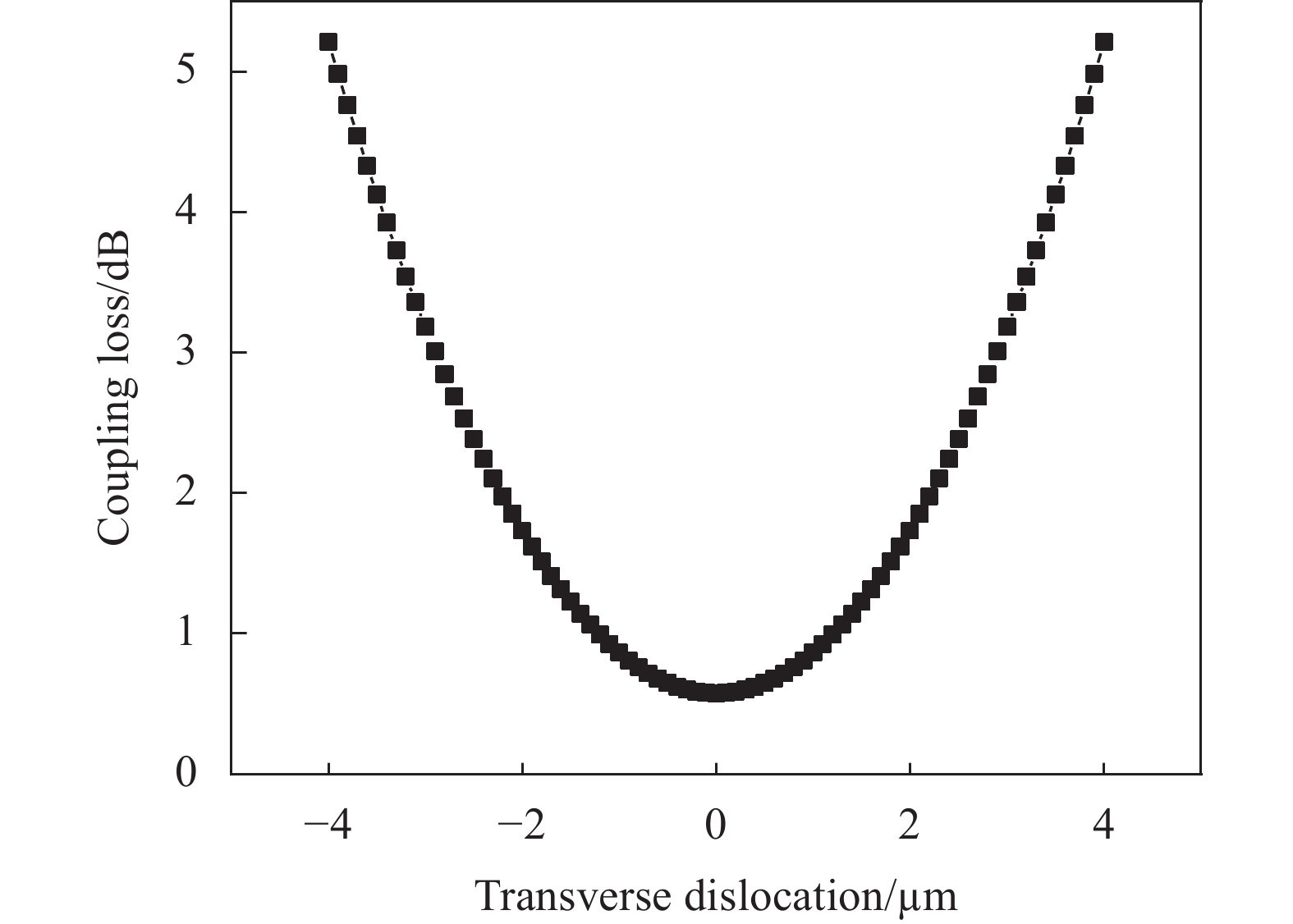
图 12 横向位错与耦合损耗的关系
Figure 12. Relationship between transverse dislocation and coupling loss
-
文中设计了一种基于SiO2、SiON锥形结构以及双层LN锥形结构的片上模斑转换器,通过理论计算和数值仿真对模斑转换器的关键参数进行了优化,在保证工艺可行性情况下, 得到如下参数设计:SiO2输入波导选择芯层折射率差0.75%,波导尺寸为6 µm×6 µm;SiON锥形波导宽端模场尺寸在2.5 µm×2.5 µm~ 3.5 µm×3.5 µm之间,对应芯层折射率在1.48~1.51之间,SiON锥形波导长度L1>250 µm且锥形尖端宽度W3在0.1~0.3 µm之间;LN平板锥形长度L2与可以在200~300 µm内变化,LN平板锥形尖端宽度W4可以在0.1~0.15 µm内变化,宽端宽度在0.8~1.4 µm内变化;LN脊型和平板构成的锥形区长度L3可以在40~100 µm内变化,脊波导锥形尖端宽度W6可以在0.1 ~0.3 µm内变化,可实现与铌酸锂薄膜波导与单模光纤的高效耦合,耦合效率在82.2%~89.0%之间,同时,得到了较高的耦合容差,有效降低了器件与单模光纤耦合难度。文中提出的基于SiO2、SiON锥形结构以及双层LN锥形结构的模斑转换器为铌酸锂薄膜光子器件的耦合和集成化提供了新方法。此外,在器件参数设计时,充分考虑后续工艺实现性,有利于后续器件的加工实现。
-
摘要: 铌酸锂薄膜光子集成技术在高速光电子领域不断凸显,被广泛用于各种片上功能实现,如电光调制、光频梳、滤波器、非线性光学频率转换器、非线性量子光源、激光器等。在铌酸锂薄膜光子集成技术发展过程中,目前面临的一个重要的技术瓶颈就是铌酸锂薄膜纳米波导与单模光纤的高效耦合。针对这一问题,设计了一种基于SiO2、SiON锥形结构以及双层铌酸锂锥形结构的模斑转换器,实现铌酸锂薄膜纳米波导与单模光纤之间模式和能量的高效传递与转换。采用三维有限差分光束传播法对器件结构进行了模拟仿真,并优化了结构参数,可实现与铌酸锂薄膜波导与单模光纤的高效耦合,耦合效率在82.2%~89.0%之间,同时,得到了±1.8 µm光纤耦合对准容差,可为下一步制备出高效耦合的铌酸锂薄膜光子器件提供参考。Abstract:
Objective The photonic integration technology based on lithium niobate thin films has become increasingly prominent in the field of high-speed optoelectronics, and is widely used for various on-chip functions, such as electro-optical modulation, optical frequency comb, filter, nonlinear optical frequency converter, nonlinear quantum light source, laser etc. In the development of lithium niobate film photonic integration technology, there is an important technical bottleneck which is the effective coupling of lithium niobate film nanowaveguides and single-mode fibers, which is also the key to hinder the practical application of lithium niobate thin film photonic devices. On-chip mode size converter is widely used in mode field transformation to realize waveguide mode field transformation. Although the existing researches have improved the coupling efficiency by using bilayer tapered waveguides or composite structures, they are all coupled with tapered fiber or thin diameter fiber, which still cannot achieve effective coupling with single-mode fiber. To solve this problem, a mode size converter based on SiO2 waveguide, SiON tapered waveguide and bilayer LN tapered waveguide is designed to achieve efficient mode and energy transfer and conversion between lithium niobate film nanowaveguide and single-mode fiber. Methods The structure of the mode size convertor composed of SiO2 waveguide, SiON tapered waveguide and bilayer LN tapered waveguide is simulated by using the three-dimensional finite difference beam propagation method, and the structural parameters of each section are sequentially optimized through optical pattern matching design and adiabatic mode transmission design, and the optical coupling efficiency and adiabatic mode conversion efficiency of each section are simulated. Results and discussions The research results show that when the refractive index difference between the core layer and cladding layer of the SiO2 waveguide is 0.75% and the size of SiO2 waveguide is 6 μm×6 μm, the coupling efficiency between SiO2 waveguide and single-mode fiber is about 93% (Fig.6). When the mode field size of the wide end of SiON tapered waveguide is 2.5 μm×2.5 μm-3.5 μm×3.5 μm, the refractive index of the corresponding core layer is 1.48-1.51, the length of the SiON tapered waveguide (L1) is greater than 250 μm and the width of the tapered tip W3 is 0.1-0.3 μm, the optical mode is gradually converted from the SiO2 waveguide to the SiON waveguide, and the conversion efficiency of the SiON tapered waveguide is 93%-97.2% (Fig.8). The bilayer LN tapered waveguide includes the LN tapered planar waveguide and the LN tapered ridge waveguide. In the LN tapered planar waveguide, when the tapering length (L2) changes in the range of 200-300 μm, the width of the tapered tip W4 changes within 0.1-0.15 μm, and the width of the wide end (W5) changes in the range of 0.8-1.4 μm, the optical mode profile in LN tapered planar waveguide increases with the increase of the inverse taper width of LN tapered planar waveguide, while that in SiON layer decreases, and the conversion efficiency of the LN tapered planar waveguide is 96%-98.5% (Fig.9). In the LN tapered ridge waveguide, when the length of LN ridge tapered waveguide (L3) varies from 40 to 100 μm, and the width of the tapered tip of LN ridge tapered waveguide W6 varies from 0.1 μm to 0.3 μm, the optical mode is gradually converted into LN ridge waveguide optical mode, and conversion efficiency of the LN tapered ridge waveguide exceeds 99% (Fig.10). Through the above design, effective coupling with lithium niobate film waveguide and single-mode fiber can be realized, and the coupling efficiency is 82.2%-89.0% (Fig.11). At the same time, ± 1.8 μm fiber coupling alignment tolerance is obtained (Fig.12). Conclusions The proposed mode size converter based on SiO2 waveguide, SiON tapered waveguide and bilayer LN tapered waveguide provides a new method for the coupling and integration of lithium niobate thin film photonic devices, which can provide a reference for the next step of preparing highly efficient coupling lithium niobate thin film photonic devices, and is beneficial to further realize the integrated application of lithium niobate devices. -
图 1 铌酸锂薄膜脊波导结构示意图
Figure 1. Schematic diagram of lithium niobate film ridge waveguide structure
图 6 SiO2波导单模条件下波导参数和波导尺寸为 6 µm×6 µm时x-y端面TE0模场分布
Figure 6. Waveguide parameters of SiO2 waveguide under single mode condition and x-y cross sectional TE0 mode field distribution of SiO2 waveguide with 6 µm×6 µm waveguide size
图 7 SiON波导单模条件及x~y端面TE0 模场分布
Figure 7. Single mode condition and x-y cross sectional TE0 mode field distribution of SiON waveguide
图 8 不同SiON锥形波导尖端宽度W1下锥形波导长度L1与转换效率关系曲线
Figure 8. Relation curve between taper waveguide length L1 and conversion efficiency under different SiON taper waveguide tip width W1
图 9 W5 和L2对III区转换效率的影响
Figure 9. The influence of W5 and L2 on the conversion efficiency in Zone III
图 10 不同锥形尖端宽度W6条件下,IV区锥形长度L3与转换效率之间关系曲线
Figure 10. Relation curve between taper length L3 and conversion efficiency in Zone IV under different taper tip width W6
图 11 设计的模斑转换器的(a)结构示意图 (b)光场传输图(c)截面光场分布图
Figure 11. (a) Structure diagram, (b) optical field transmission diagram and (c) cross section optical field distribution diagrams of designed spot size converter
-
[1] Wang C, Zhang M, Chen X, et al. Integrated lithium niobate electro-optic modulators operating at CMOS-compatible voltages [J]. Nature, 2018, 562(7725): 101-104. doi: 10.1038/s41586-018-0551-y [2] Morton P A, Khurgin J B, Morton M J. All-optical linearized Mach-Zehnder modulator [J]. Optics Express, 2001, 29(23): 37302-37313. [3] 孙时豪, 蔡鑫伦. 高性能硅和铌酸锂异质集成薄膜电光调制器(特邀)[J]. 红外激光与工程, 2021, 50(7): 20211047. doi: 10.3788/IRLA20211047 Sun Shihao, Cai Xinlun. High-performance thin-film electro-optical modulator based on heterogeneous silicon and lithium niobate platform (Invited) [J]. Infrared and Laser Engineering, 2021, 50(7): 20211047. (in Chinese) doi: 10.3788/IRLA20211047 [4] Gao R, Yao N, Guan J, et al. Lithium niobate microring with ultra-high Q factor above 108 [J]. Chinese Optics Letters, 2022, 20(1): 011902. doi: 10.3788/COL202220.011902 [5] Gao R, Zhang H, Bo F, et al. Broadband highly efficient nonlinear optical processes in on-chip integrated lithium niobate microdisk resonators of Q-factor above 108 [J]. New J Phys, 2021, 23(12): 123027. doi: 10.1088/1367-2630/ac3d52 [6] Zheng Y, Chen X. Nonlinear wave mixing in lithium niobate thin film [J]. Advances in Physics: X, 2021, 6(1): 1889402. doi: 10.1080/23746149.2021.1889402 [7] Lin J, Yao N, Hao Z, et al. Broadband quasi-phase-matched harmonic generation in an on-chip monocrystalline lithium niobate microdisk resonator [J]. Phys Rev Lett, 2019, 122(17): 173903. doi: 10.1103/PhysRevLett.122.173903 [8] Xu B Y, Chen L K, Lin J T, et al. Spectrally multiplexed and bright entangled photon pairs in a lithium niobate microresonator [J]. Sci China-Phys Mech Astron, 2022, 65(9): 294262. doi: 10.1007/s11433-022-1926-0 [9] Xue G T, Niu Y F, Liu X, et al. Ultrabright multiplexed energy-time-entangled photon generation from lithium niobate on insulator chip [J]. Phys Rev Appl, 2021, 15(6): 064059. doi: 10.1103/PhysRevApplied.15.064059 [10] Lin J, Farajollahi S, Fanget Z, et al. Electro-optic tuning of a single-frequency ultranarrow linewidth microdisk laser [J]. Adv Photon, 2022, 4(3): 036001. [11] Zhang P, Huang H, Jiang Y, et al. High-speed electro-optic modulator based on silicon nitride loaded lithium niobate on an insulator platform [J]. Optics Letters, 2021, 46(23): 5986-5989. doi: 10.1364/OL.446222 [12] Wang C, Zhang M, Yu M J, et al. Monolithic lithium niobate photonic circuits for Kerr frequency comb generation and modulation [J]. Nature Communications, 2019, 10(1): 978. doi: 10.1038/s41467-019-08969-6 [13] Zhang M, Buscaino B, Wang C, et al. Broadband electro-optic frequency comb generation in a lithium niobate microring resonator [J]. Nature, 2019, 568(7752): 373-377. doi: 10.1038/s41586-019-1008-7 [14] Pohl D, Escalé M R, Madiet M, et al. An integrated broadband spectrometer on thin-film lithium niobate [J]. Nat Photonics, 2020, 14(1): 24-29. doi: 10.1038/s41566-019-0529-9 [15] He L, Zhang M, Shams-Ansari A, et al. Low-loss fiber-to-chip interface for lithium niobate photonic integrated circuits [J]. Optics Letters, 2019, 44(9): 2314-2317. doi: 10.1364/OL.44.002314 [16] Hu C, Pan A, Li T, et al. High-efficient and polarization independent edge coupler for thin-film lithium niobite waveguide devices[EB/OL]. (2020-09-07)[2022-12-27]. https://arxiv.org/abs/2009.02855. [17] Pan Y, Heyun T, Zhang J, et al. Low-loss edge-coupling thin-film lithium niobate modulator with an efficient phase shifter [J]. Optics Letters, 2021, 46(6): 1478-1481. doi: 10.1364/OL.418996 [18] Press W H, Flannery B P, Teukolsky S A, et al. Numerical Recipes: The Art of Scientific Computing[M]. 3rd ed. New York: Cambridge University Press, 1986: 156-163. [19] Rsoft Design Group. Beam PR, OP7.0 user guide[Z]. Ossining: Rsoft Design Group Inc, 2006. [20] Hadley G R. Transparent boundary condition for beam propagation method [J]. Optics Letters, 1991, 16(9): 624-626. doi: 10.1364/OL.16.000624 [21] Hadley G R. Transparent boundary condition for the beam propagation method [J]. IEEE Journal of Quantum Electronics, 1992, 28(1): 363-370. doi: 10.1109/3.119536 [22] Vassalo C, Collino F. Highly efficient absorbing boundary condition for the beam propagation method [J]. Journal of Lightwave Technologyvol, 1996, 14(6): 1570-1577. doi: 10.1109/50.511688 [23] Huang W P, Xu C L, Lui W, et al. The perfectly matched layer (PML) boundary condition for the beam propagation method [J]. IEEE Photonics Technology Letters, 1996, 8(5): 649-651. doi: 10.1109/68.491568 [24] Chiou Y P, Chang H C. Complementary operators method as the absorbing boundary condition for the beam propagation method [J]. IEEE Photonics Technology Letters, 1998, 10(7): 976-978. doi: 10.1109/68.681289 -

 点击查看大图

计量
- 文章访问数: 275
- HTML全文浏览量: 77
- PDF下载量: 75
- 被引次数: 0

