


-
单光子探测器是一种可检测单个光子能量(约10−19 J)的高灵敏度器件。按工作原理不同,单光子探测器可分为光电倍增管(Photomultiplier Tubes,PMT)、超导单光子探测器(Superconducting Single Photon Detectors,SSPD)和单光子雪崩光电二极管 (Single-photon Avalanche Diodes,SPAD)。光电倍增管利用真空管中电场加速来实现电子倍增,缺点是暗计数较大,而且由于高压组件使得器件尺寸较大。超导单光子探测器主要包括超导纳米线单光子探测器(Superconducting Nanowire Single Photon Detectors, SNSPDs)和超导转变边沿单光子探测器(Transition Edge Sensors,TESs)。这种探测器利用超导材料吸收光子后的状态变化来进行信号检测,可以获得高达98%的单光子探测效率[1]。但为了保证超导状态,需要大体积制冷装置,难以实现大规模阵列化。
SPAD是一类利用半导体材料内部载流子的雪崩倍增效应实现高灵敏度探测的光电器件,工作在盖革模式,其工作电压高于击穿电压,内部增益可达到106~108,可进行单光子级信号探测[2]。目前,技术相对成熟的是Si材料SPAD和InGaAs材料SPAD。InGaAs材料SPAD在0.9~1.7 μm光谱范围内有高量子效率,是1.06、1.55 μm主动激光探测的理想探测器。InGaAs单光子雪崩焦平面基于阵列化技术,将高效率InGaAs SPAD阵列芯片与CMOS计时/计数读出电路芯片集成封装,可对光子信号进行时间量化,具有高灵敏、高精度、小体积、全固态的特点,在激光三维成像[3-4]、远距离激光通信[5-6]、稀疏光子探测[7]等领域应用广泛,是近年来单光子探测领域的研究。
InGaAs单光子雪崩焦平面在20世纪90年代后期由美国麻省理工学院林肯实验室率先开始研究[8],国外研制机构包括Princeton Lightwave(后被Argo AI收购)[9]、Boeing Spectrolab[10]、Ball Aerospace[11]等。2002年至今,国外陆续报道了32×32[12]、128×32以及256×64等不同规格InGaAs雪崩焦平面探测器,并应用在Jigsaw[13]、ALIRT[14]、HALOE[15]、MACHEET、AOSTB[16]等验证样机中,实现了机载隐身目标三维成像、机载高精度地形测绘等应用,扫描速度可达1000 km2/h,相比传统基于线性APD成像系统,其速度提高了10倍以上,在降低系统质量、功耗、体积上优势明显[15]。国内近几年发展也较为迅速,研究机构包括重庆光电技术研究所、西南技术物理研究所和中国科学院上海技术物理研究所等单位。2016年,哈尔滨工业大学孙剑锋团队与重庆光电技术研究所合作,基于32×32 InGaAs单光子雪崩焦平面搭建了一套1570 nm激光主动成像实验平台,获得了3.9 km目标轮廓像[17]。2020年,华东电子工程研究所葛鹏团队通过建立目标反射率与距离的极大似然估计,采用国内面阵单光子探测器对室外600 m外目标进行了成像[18]。
文中首先介绍了InGaAs单光子雪崩焦平面的结构及基本原理,结合笔者单位工作回顾了国内外单光子雪崩焦平面技术的研究进展,并对未来技术发展进行了讨论和展望。
-
InGaAs单光子雪崩焦平面通常采用PGA封装(Pin Grid Array Package,PGA),结构示意图如图1所示。InGaAs SPAD阵列芯片和CMOS读出电路经铟柱倒装互连,并与微透镜进行耦合。芯片贴装在陶瓷基板上,TEC制冷器(Thermo Electric Cooler,TEC)对芯片进行制冷,降低芯片温度。管壳与阵列芯片通过金丝进行电连接。入射光子经芯片汇聚到吸收层有源区,被吸收后转化成电子-空穴对,载流子在内部电场作用下迁移到倍增层。由于InGaAs SPAD阵列芯片工作在击穿电压之上的过偏压盖革模式下,倍增层高电场促使载流子在倍增层迅速碰撞离化引发雪崩,产生宏观电流并传输到CMOS读出电路。CMOS读出电路提供像素级电接口,对单像素产生的雪崩电流进行检测并淬灭,输出经时间量化的信号。微透镜通过高精度对准连接到背照式SPAD阵列芯片,确保高填充因子。InGaAs单光子雪崩焦平面的核心是SPAD阵列芯片和CMOS读出电路芯片,直接决定了器件的性能。

图 1 InGaAs单光子雪崩焦平面结构示意图
Figure 1. Structure diagram of APD single-photon avalanche focal plane array
-
InGaAs SPAD阵列芯片的纵向器件结构通常采用的是吸收层、能带渐变层、电场控制层和雪崩倍增层分离的SAGCM外延结构,可以在InP衬底之上依次顺序(顶部为P型接触层的P-i-N结构)或者逆序排列(顶部为N型接触层的N-i-P结构)。各功能层作用如下:(1)吸收层根据入射光的工作波长,InGaAs材料的禁带宽度为0.74 eV,长波截止吸收波长为1.7 μm。(2)电场控制层用于调控纵向电场分布,通过提高倍增层电场促进雪崩碰撞离化,抑制吸收层电场降低隧穿概率。通常电荷浓度越高,倍增层与吸收层电场差异越大;(3)过渡层主要是降低吸收层载流子向倍增层渡越的价带势垒,消除异质界面结空穴积累效应;(4)倍增层使得载流子在其中发生雪崩碰撞离化从而实现高增益,采用的InP(Eg~1.35 eV)材料,倍增层厚度一般在0.8~1.4 μm。
InGaAs SPAD阵列芯片的横向器件结构主要分为平面型和台面型两种。
(1)平面型SPAD器件结构通常采用掩埋P-N结,通过光刻SiNx介质膜图形来确定Zn掺杂的扩散区域以及有源区,并使用两次扩散来调整P-N结轮廓,以使结在有源区的中心部分比在结外围更深,这种设计确保了有源区中心部分的增益分布是均匀的,且高于边缘外围区域增益,确保边缘击穿抑制、低暗电流(<1 nA)和高可靠性。在阵列像元间刻蚀了深度达到缓冲层的隔离槽,一方面防止像素阵列间二次电致光子的光学串扰,另一方面阻断吸收层载流子横向的电学串扰[19]。平面结构还包括了与像元有源区中心对准的正面In柱和背面增透膜,分别用于CMOS读出电路倒装互连和探测器芯片背照进光。倍增层需使用扩散及掺杂工艺,因此平面结构采用倍增层在上,吸收层在下的P-i-N结构,如图2所示。

图 2 平面型SPAD芯片结构示意图
Figure 2. Schematic diagram of planar SPAD chip structure
(2)台面型SPAD器件结构的P-N结通过外延生长而成,吸收区在倍增区上方,如图3所示。与通过扩散掺杂来限定有源区的平面结构不同的是,其有源区边缘由台面的蚀刻结构确定。台面刻蚀工艺一般选用各向同性的非选择性腐蚀溶液进行湿法刻蚀,能够在侧壁形成光滑连续坡面。一方面,该坡面便于有机和无机介质在侧壁表面形成良好覆盖,提高钝化效果;另一方面,该斜坡结构能够增大底部倍增层横向宽度,利用中心有源区到边缘的距离,降低高电场倍增层侧壁边缘的电场,减小暗电流。台面结构设计通常采用n+型InP衬底,除台面以外的材料都会被去湿法刻蚀除掉,形成相互隔离的像元[20]。
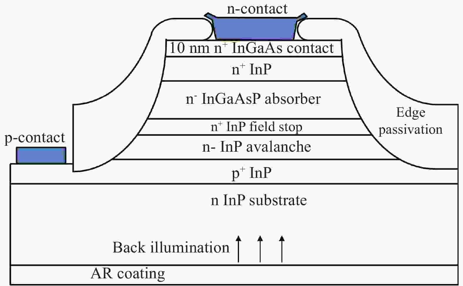
图 3 台面型SPAD芯片结构示意图
Figure 3. Schematic diagram of mesa-type SPAD chip structure
-
CMOS读出电路的功能是用于检测、时间量化以及淬灭SPAD芯片产生的雪崩信号,是实现器件功能的重要部分。InGaAs单光子雪崩焦平面的读出电路最早由林肯实验室开发[8],其基本框图结构如图4所示。CMOS读出电路芯片的单像素电路包括前端电路、计时电路(Timing Circuit)和用于控制像素工作状态的像素控制电路(Pixel Controller)。前端电路包括:为SPAD提供电压偏置的偏置电路(Arm Circuit)、用于快速检测雪崩事件的鉴别器电路(Discriminator)以及淬灭电路(Quench Circuit)。计时电路用于光子飞行时间-数字转换,其输入与鉴别器的输出相连。像素控制器相当于有限状态机,用于控制SPAD偏置到过偏压状态、低功耗等待状态、非使能状态等。当前端电路检测到雪崩事件后,淬灭电路快速淬灭SPAD并进入等待状态,经过预设时间后像素控制电路控制SPAD进入过偏压状态,预设时间的长短将直接影响后脉冲的发生概率。

图 4 读出电路基本框图
Figure 4. Basic block diagram of ROIC
-
InGaAs单光子雪崩焦平面的关键指标包括阵列规模、像元中心距、探测效率、暗计数率、时间抖动、累积串扰概率、时间分辨率等。下面围绕这些指标,从SPAD阵列芯片、读出电路两方面的进展进行介绍。
-
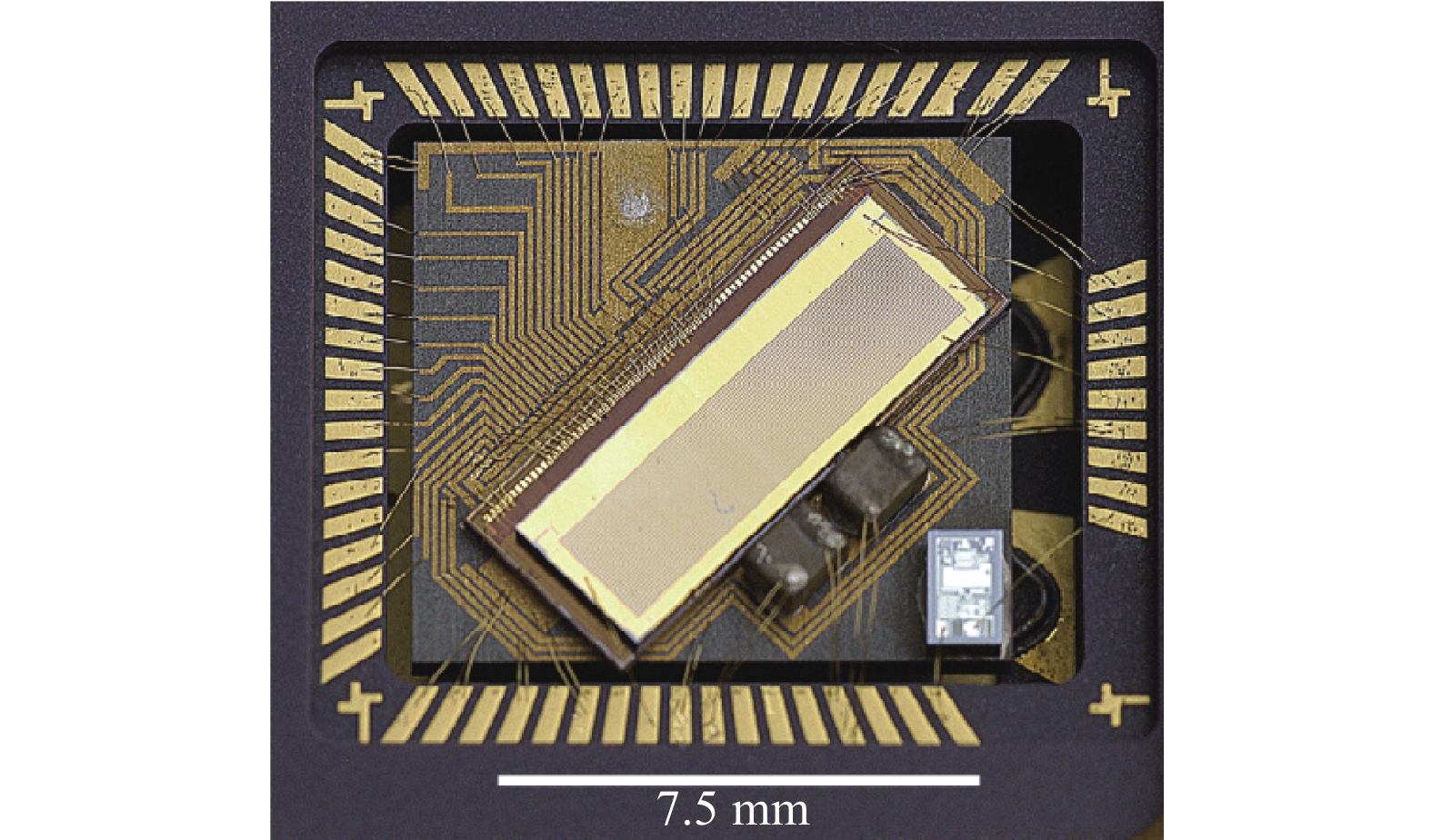
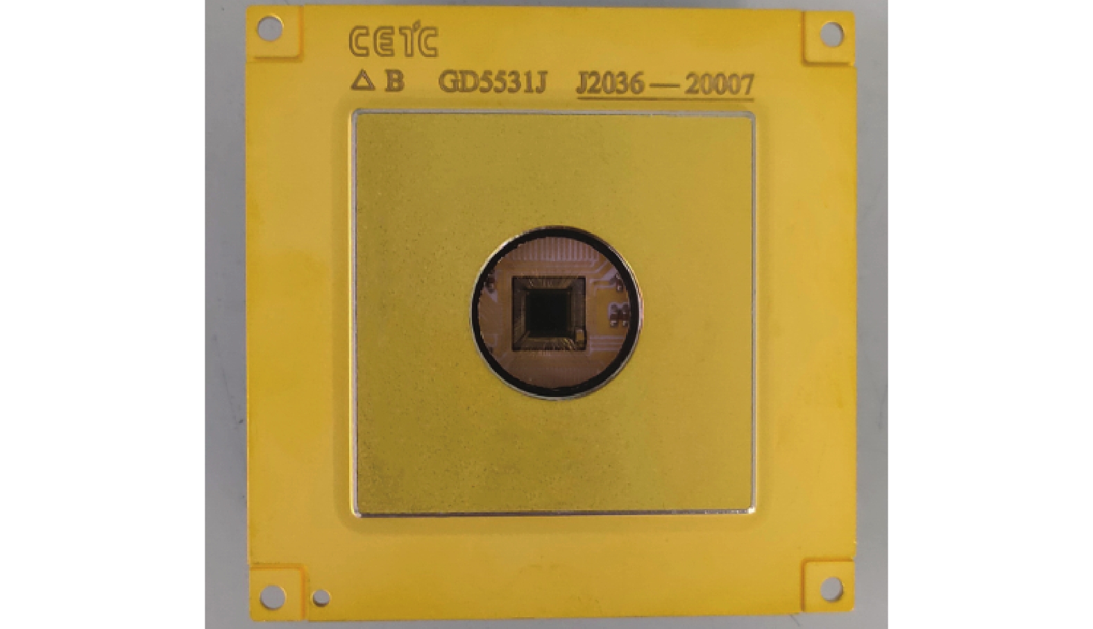
SPAD阵列芯片的阵列规模和中心间距决定了器件的空间分辨率。更大阵列规模、更小中心间距可以获得更清晰的目标信息。早期MIT-LL的Heinrichs等人采用桥接互连方式,将单个CMOS读出电路芯片与SPAD晶圆通过环氧树脂面对面贴合。这种方式通过水平爬坡电极将CMOS读出电路芯片与SPAD芯片进行电连接,占用面积较大[21]。2011年,Itzler等人研制了128×32规格InGaAs单光子雪崩焦平面[22],该器件通过器件结构优化及铟柱互连的方式缩小了像元尺寸,像元间距减小到50 μm ,如图5所示。Younger等人新设计器件的目标是将像元间距进一步减小到25 μm[23],阵列规模为256×256。国内方面,重庆光电技术研究所研制的64×64 InGaAs单光子雪崩焦平面如图6所示,像元间距为50 μm,探测效率20%,暗计数率10 kHz,时间分辨率小于1 ns,目前已成功扩展到256×64,性能参数如表1所示。

图 5 128×32 InGaAs单光子雪崩焦平面
Figure 5. 128×32 InGaAs single-photon avalanche focal plane array

图 6 64×64 InGaAs单光子雪崩焦平面
Figure 6. 64×64 InGaAs single-photon avalanche focal plane array
表 1 InGaAs单光子雪崩焦平面参数
Table 1. Parameters of InGaAs single-photon avalanche focal plane array
Institute Array scale Photo detection efficiency Dark count/kHz Operating temperature/K MIT-LL
PLI
CETC 44th
CETC 44th256×128 40% 20 ~250 128×32
64×64
256×6420%
20%
30%10
10
20~248
~243
~243大阵列小间距SPAD阵列芯片的发展主要受限于小间距的单元器件设计和阵列芯片工艺。主要手段包括:(1)采用高效率光敏芯片结构设计,并缩小像元尺寸;(2)采用像元间有效隔离结构抑制串扰;(3)采用高质量表面钝化降低暗电流;(4)采用高质量外延及结扩散工艺,保证阵列芯片一致性;(5)提高小像元下微透镜的耦合效率。
-
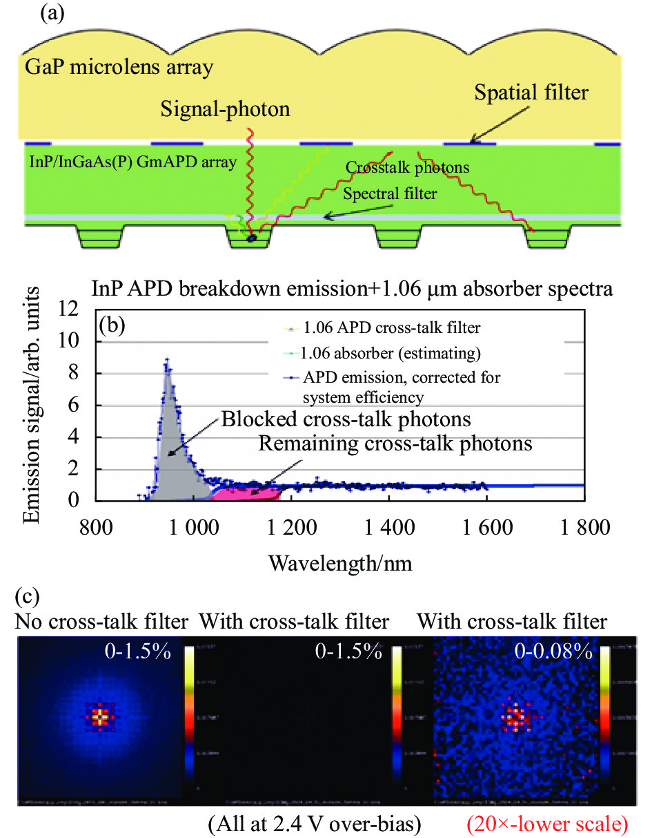
对于大阵列器件,串扰是影响成像质量的重要因素。由于SPAD的高增益特性,邻近像元产生的极少量光子或漂移电流都可能导致雪崩触发。串扰主要来源于电串扰和光串扰。像元间的深槽可以有效隔离电串扰。而光串扰主要来源于入射杂散光、邻近像元的倍增区中热载流子荧光辐射的次级光子,这些非信号光通过背面反射和横向渡越传播到相邻像元,如图7(a)所示。倍增区中热载流子荧光辐射光谱主要分布在900~1000 nm附近,如图7(b)所示。Acerbi等人采用平面隔离沟道的方式,将串扰概率控制在5%~15%左右[24]。2009年,Younger等人通过在阵列芯片上设置光谱滤波层和空间滤波层的方法,用光谱滤波层直接将950 nm范围附近的荧光辐射次级光子吸收掉,配合空间滤波层减少串扰光子数,使过偏压2.4 V下的串扰从~1%降低至~0.1%,串扰概率下降了1个数量级[25],如图7(c)所示。但在高偏压下,依然存在串扰概率大的问题。2018年,Diagne等人进一步开发了结合衬底移除的像元隔离技术,实现像元正面和背面的完全隔离,切断了次级光子传播的路径,使串扰概率下降约150倍,同时将光谱响应拓展到可见光波段[26] 。2020年,Yuan等人基于III-V族化合物工艺平台研制的InGaP盖革雪崩焦平面,也采用了该像元隔离技术,使雪崩焦平面在高探测效率下,仍然能够有效抑制阵列像素的串扰[27]。

图 7 (a)串扰来源示意图;(b) SPAD自发辐射光谱;(c)串扰抑制
Figure 7. (a) Schematic diagram of crosstalk; (b) SPAD spontaneous emission spectrum; (c) Crosstalk suppression results
-
为提升InGaAs单光子雪崩焦平面的探测效率、暗计数等性能参数,研究人员做了诸多努力。探测效率方面,Donnelly等人通过建立数学模型,详细分析了SPAD器件结构中各材料层参数对光电性能的影响[28]。重庆光电技术研究所设计了一种增强吸收SPAD结构,将单光子探测效率提升了20%,最高探测效率达到60%[29]。
在减少暗计数方面,提高外延材料质量也是实现高性能器件的重要方式。Chapman等人研究了有机金属气相外延的生长温度、生长速率和V/III比值等工艺条件,使InGaAsP/InP材料300 K下的暗计数降低44% [30]。
-
InGaAs单光子雪崩焦平面是一种光子信号到数字信号转换的阵列探测器,针对光子信号的种类与获取频率等不同功能的定制方案可以满足多种不同的应用需求,包括激光雷达、超远距离激光通信和稀疏光子成像等。其中读出电路芯片是不同方案的主要差异,其负责完成焦平面除光电转换外的其他功能的定义与实现。
-
快闪型激光雷达系统通过用激光短脉冲照射目标场景并在焦平面上接收反射回来的激光脉冲信号完成成像,焦平面上每个像素独立完成回波脉冲的“光子飞行时间”测量,经数据算法处理后获得空间深度三维图像。其中激光回波的探测由SPAD阵列芯片实现,其输出行为近似于光控数字开关,有光时输出为“1”,无光时输出为“0”,即便是单个“光子”量级的信号,其响应速度也可达皮秒级,因此,其极其适合需要精确量化“光子飞行时间”的应用[31]。像素电路实现类似计时秒表功能,激光发射时开始计时,在检测到回波光子事件后停止计时,在激光脉冲之间的时间间隔(数十微秒级)中读出计时数据,较长的时间间隔可以有效抑制后脉冲,但也会导致激光雷达用焦平面只能工作在低时间占空比情况下。
用于激光雷达的阵列读出电路像元结构如图8所示。读出电路采用数字计数器记录计时时钟周期个数的原理完成时间测量,但是时钟频率会限制时间精度;为了降低计时时钟频率,采用带游标位的多段时间-数字转换器方案实现时钟相位的细计数,完成亚ns级以上的计时精度;计时时钟采用500 MHz,细计数采用4相位就可以实现0.5 ns的分辨率[32]。

图 8 激光雷达用像素电路原理结构图
Figure 8. Schematic diagram of pixel circuit for Lidar
随着阵列规模的扩展,能效比提升在读出电路架构设计中的重要性逐步增加。目前读出电路的主流工艺节点为180 nm CMOS[33]。相比早期的读出电路架构(350 nm),其能效比得到大幅提高。在远距离激光雷达应用中,每帧的光子事件比较稀疏,三维图像通常使用多个帧的叠加处理来构建。最新的读出电路架构设计中利用了这种稀疏检测的特性,计时电路采用光子事件驱动计时的方案,只有检测到光子事件的像素计时电路才开始计时工作,所有像素统一结束计时,并在读出状态读出像素数据。读出中还在读出数据流中设计数据减薄算法,使功耗、数据量与阵列中活动像素数成正比。传统方案由于功耗限制其帧频只设计到20 kf/s的帧速率,而该方案的帧速率可以随着光子事件越来越稀疏而增加,在每帧有1000个光子事件的稀疏度下,最大可以接近150 kf/s的帧速率,同时大幅降低功耗[33]。
高时间分辨率和高帧频带来了更高的测绘精度和扫描速度。2011年,MIT林肯实验室开发的机载激光雷达成像研究试验台(ALIRT),采用128×32 InGaAs单光子雪崩焦平面,在海拔9000 m下对大峡谷(高程差1000~2500 m)进行快速高分辨率广域地形测绘,扫描速度达到2 000 km2/h、分辨率可以达到10 cm级[14],可以清晰分辨轮廓细节(图9)。2017年,MIT林肯实验室基于256×64 InGaAs单光子雪崩焦平面开发了机载光学系统试验台(AOSTB),实现了对哈维飓风救灾现场的快速成像,目标分辨率精度达到0.25 m[16]。

图 9 美国大峡谷的激光雷达成像图
Figure 9. Lidar image of the Grand Canyon
-
InGaAs单光子雪崩焦平面还可作为自由空间光通信链路的接收机,利用脉冲位置调制(PPM)格式完成发射信号调制,接收到的到达时间数据用于数据解调。相比于经典的相干通信系统,其接收机具有捕获跟踪通信一体化、体积小、探测灵敏度高的优点,在超远距离激光通信优势明显,NASA已用于火星激光通信MLCD (约2亿公里)、月地激光通信LLCD (约40万公里)等验证项目,激光通信系统及接收链路如图10所示。
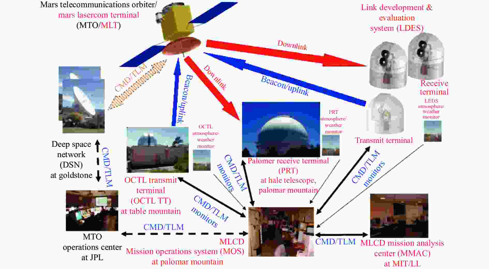
图 10 激光通信系统及接收链路示意图
Figure 10. Diagram of laser communication system and receiving link
2013年,NASA完成了世界上第一个月球轨道与地面的双向激光通信链路,采用基于8×8异步读出InGaAs单光子雪崩焦平面的小型化激光终端(FLT),最高上行传输速率达到622 Mbps[34]。同期,NASA近地应用高速激光通信旗舰项目—激光通信中继演示项目(LCRD),其飞行有效载荷托管在一颗商业通信卫星上,由太空中的两个激光通信终端组成,同时支持近地激光通信和深空激光通信。
与激光雷达用读出电路一样,激光通信用读出电路同样需要完成高精度的时间量化功能。然而光通信应用中信号光子到达的时间间隔平均比激光雷达脉冲之间的时间短三个数量级,这就需要更短读出时间与更大数据量,否则会导致光子信号的堵塞现象。
为了解决这一问题,林肯实验室于2004年报道了基于事件驱动读出方法设计的8×8光子计时异步读出电路阵列[35]。在每个PPM帧中,像素采用与激光雷达读出电路相同的方法标记光子到达时间。当每一行像素需要读出时,仅将发生光子事件的像素串入读出数据流。当下一个PPM帧开始时,没有获取光子事件的像素仍然处于活动状态,而上一帧获取光子事件的像素则进入等待模式以便抑制后脉冲。该芯片采用350 nm CMOS工艺技术制造并与一个8×8 SPAD阵列混合集成。在美国宇航局火星激光通信演示系统中,在非常高的背景光干扰的情况下,实现了每个光子两位的数据速率[36]。
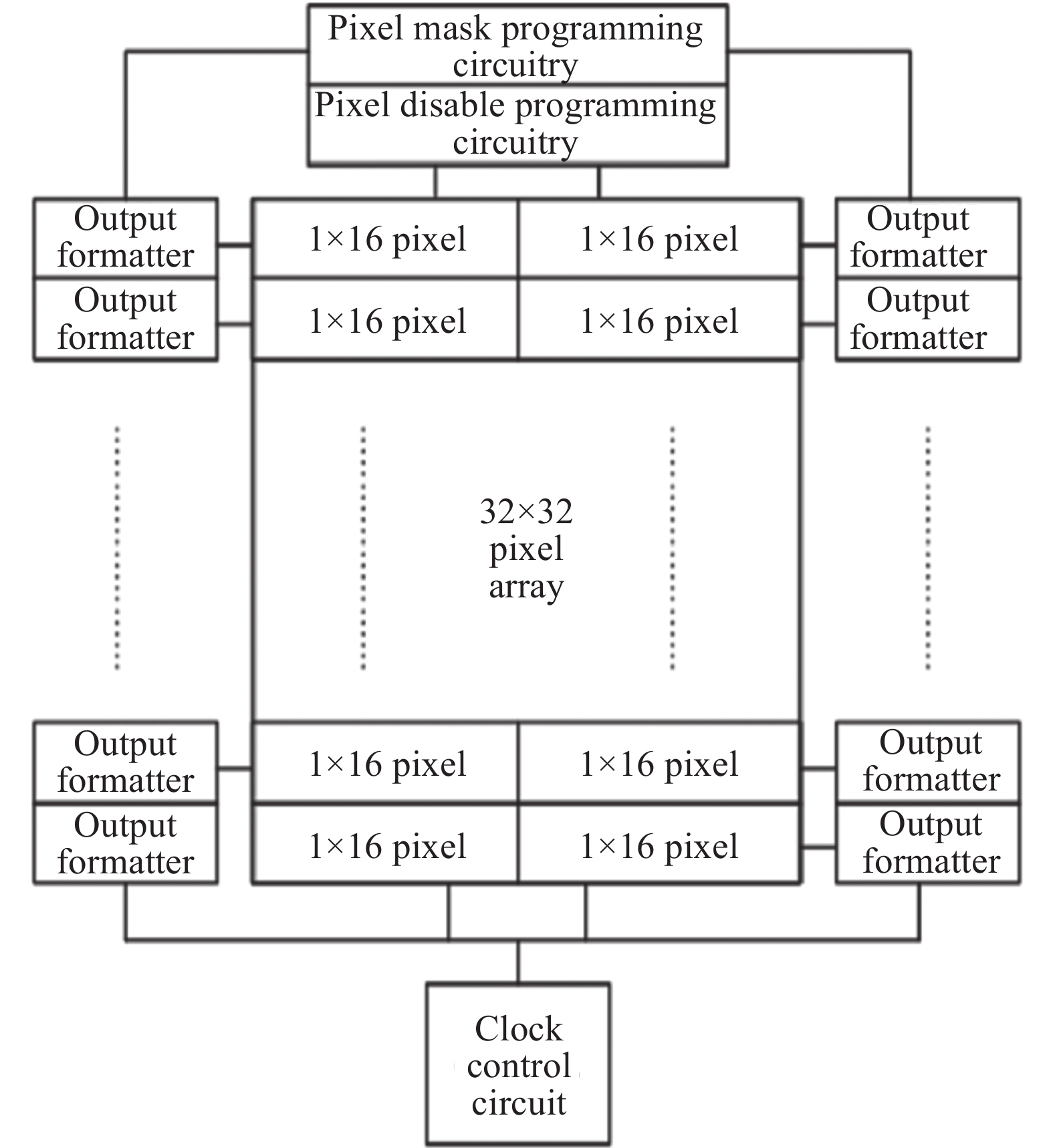
和激光雷达用读出电路的情况一样,激光通信用读出电路同样需要扩展到更大的阵列,并抑制功耗的增加。这一需求推动下,国外已经开发出32×32阵列的规格产品,并继续开发256×256等更大规格阵列。32×32异步读出电路体系结构如图11所示,通过引入像素禁用、感兴趣区域、计时信息与空间位置信息分开等方案与手段,进一步提高的事件驱动读出的能效比。

图 11 32×32异步读出电路体系结构框图
Figure 11. Architecture block diagram of 32×32 asynchronous ROIC
该设计方案中,每个像素都包含计时信息与空间位置信息两种数据信息,每一行数据读出时会分为两个数据流。第一个数据流是显示所有光子事件的像素位置图,第二个是带有嵌入位置信息的计时数据包。该读出电路还具有像素禁用选项,可以指定任一像素只输出像素位置图数据,而不输出时间信息,这些特性可用于在不需要全部像素数据时减少功耗与输出数据量。
-
雪崩焦平面的另一类应用是统计到达每个像素上的光子个数。这些应用不需要精确的计时分辨率,而是需要高探测效率和低暗计数率。传统的焦平面或图形传感器是通过每帧内测量一段积分时间的光子个数来进行强度测量,通过调节积分电容大小完成增益调节;基于盖革模式的被动成像也类似,通过对一段固定时间的光子数进行多次测量完成积分过程,统计叠加生成强度测量数据,其可以通过调节固定时间大小实现近似增益调节。
稀疏光子成像用读出电路中的每个像素都有一个计数器代替其他读出电路中的计时电路,当检测光子事件发生时,该计数器会增加计数。其难点是降低像素面积并提高阵列规模;降低像素面积一般通过改进计数器结构与更先进的流片工艺实现;另一个难点是提高动态范围,文献中报道了多种方案包括计数溢出位[37]、多统计时间数据叠加[38]等。
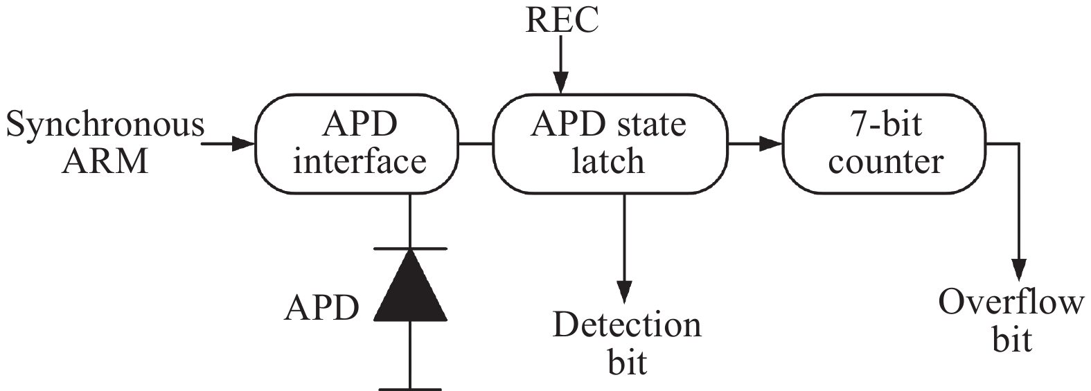
图12所示为典型的溢出位被动成像读出电路结构,包括SPAD接口电路、SPAD状态寄存电路及7 bit计数器。接口电路与其他读出电路类似,包括偏置与检测电路;状态寄存电路存储每段统计时间的SPAD状态信息;计数器记录每帧光子事件的达到次数,计满后复位重新开始计数,溢出位记录计数器计满的状态,积分中单独读出后复位;读出的数据通过行列寻址读出到像素外相应像素的存储位,积分中累加的值作为该像素高位计数数据。在积分结束时,如果7位计数器的数据对像素外高位数据值的贡献小于暗噪声,则可以读出或丢弃7位计数器中的残余数据。该溢出读出方案有效地扩展了像素中计数位数。

图 12 带溢出位被动成像读出电路结构示意图
Figure 12. Architecture diagram of passive imaging ROIC with overflow bit
-
激光雷达、远距离激光通信、稀疏光子成像以及未来新应用场景,对更大规模、更小像素、更高性能,以及更多功能的InGaAs单光子雪崩焦平面提出了要求。为了实现百万像素级InGaAs单光子雪崩焦平面,需要面对SPAD阵列芯片、读出电路芯片、封装互连方式等诸多挑战,具体包括:
(1) SPAD阵列芯片方面,未来InGaAs单光子雪崩焦平面的阵列规模会达到1 k×1 k以上。为了在高密度、小尺寸像元下还能实现高增益、高计数率、低噪声、低串扰,需要研究一些新型器件结构设计,如纳米SPAD结构、集成负反馈电阻结构(NFAD)、瞬态载流子势垒层(TCB)自淬灭结构、集成微谐振腔结构等。为了提高视场角和填充因子,超透镜、自由曲面透镜等新型微透镜类型也在研究中。同时,阵列均匀性也是需要重点关注的问题。MIT-LL已经验证了6 in (1 in=2.54 cm) InP晶圆工艺在提高SPAD阵列均匀性方面的优势,未来在6 in InP工艺平台上实现3D集成、高密度封装变得越来越有吸引力。
(2)受限于SPAD芯片的浅制冷工作环境和读出电路本身的特点,读出电路的设计受到挑战主要有三点如下:1) 动态功耗问题,读出电路存在功耗周期性大幅跳变的特点,导致其动态功耗远大于同等规模的其他大规模集成电路,功耗大幅跳变会导致电源电压极度不稳定,造成数据丢失和损坏等问题;2) 深亚微米工艺的偏置电压问题,标准深亚微米工艺中一般只能提供3.3 V的IO电压,无法满足SPAD阵列芯片高探测效率和小像素的应用需求;3) 总输出带宽,读出电路的最大数据量随着阵列规模增长线性增长,大阵列高帧频带来超大数据量读出必定会带来功耗、工艺、设计复杂度等问题。
(3)面对一些新的探测需求,如可重构探测、主被动复合探测等,InGaAs单光子雪崩焦平面的发展需要不断融合创新架构、创新算法。目前国际上已经出现了多种新型读出电路架构以及针对偏置电压和像素小型化问题提出了SPAD芯片、模拟电路与数字电路采用不同工艺三维异质集成封装方案、工艺限制下采用低压晶体管串联叠加实现高偏置电压像素电路方案等;针对芯片IO高输出带宽问题提出了多帧叠加计时直方图数据减薄算法[39]、低误码数据压缩算法等;针对多功能需求,提出了多功能复合读出电路,一种是局部多功能方案,全局像素功能是统计光子个数,局部选择区域像素实现光子计时或异步光子计时[40]。另一种是不同功能对应不同分辨率,全分辨率像素功能是统计光子个数,相邻像素合并大像素后实现光子计时功能。
-
作为一种高灵敏度、高时间分辨率的探测器,InGaAs单光子雪崩焦平面在激光三维成像、远距离激光通信、稀疏光子探测等领域已成功应用。InGaAs单光子雪崩焦平面采用半导体工艺,在阵列扩展、功能扩展方面有明显优势。文中从器件结构设计、芯片工艺、电路设计等方面对InGaAs单光子雪崩焦平面进行了分析介绍,并对未来百万像素级焦平面技术发展进行了展望。
Research progress of InGaAs single-photon avalanche focal plane (invited)
-
摘要: 雪崩光电二极管(APD)是一种高灵敏度光电器件。按照工作电压的不同可分为线性APD和盖革APD。其中,盖革APD的工作电压高于击穿电压,利用半导体材料内部载流子的高雪崩增益可实现单光子级信号探测,也被称为单光子雪崩光电二极管(SPAD)。InGaAs材料SPAD在0.9~1.7 μm光谱范围内有高量子效率,是1.06、1.55 μm主动激光探测的理想探测器。通过将高效率InGaAs SPAD阵列芯片与CMOS计时/计数读出电路芯片集成封装,制备的雪崩焦平面探测器可对光子信号进行时间量化,在三维激光雷达、远距离激光通信、稀疏光子探测等领域有广泛应用。介绍了InGaAs单光子雪崩焦平面的器件结构及基本原理,在此基础上回顾了国内外雪崩焦平面技术的研究进展,并对未来发展方向进行了展望。Abstract:
Significance Single photon detector is a kind of highly sensitive device that can realize single-photon-level signal detection. Compared with photomultiplier tubes (PMT) with large dark counts rate and large device sizes and superconducting single photon detectors (SSPD) with large-volume refrigeration devices and difficult integration into arrays, the single-photon avalanche photodiode (SPAD) with small size and easy integration into arrays exhibit the advantages of high speed, high sensitivity and high quantum efficiency. InGaAs has the characteristics of direct band gap, large ionization coefficient ratio and lattice constant matching with InP, which is currently the infrared detector material with the best performance in the near-infrared band. And InGaAs/InP SPAD is an ideal detector for active laser detection at 1.06 μm and 1.55 μm. Through the integrated packaging of high-efficiency InGaAs SAPD array and counting CMOS readout integrated circuit (ROIC), the obtained InGaAs SAPD focal plane detector has the characteristics of high sensitivity, high accuracy, small size, and solid-state packaging. The device has been widely used in 3D LIDAR, deep-space laser communication, sparse photon detection and other fields and a research hotspot in the field of single-photon detection in recent years. Progress The research progress of InGaAs SAPD focal plane detector can be illustrated by the performance improvement of SPAD array chip and the application progress of ROIC. And the research progress of SPAD array chip includes the research progress of array scale and pixel center distance, crosstalk suppression, photo detection efficiency (PDE) and dark count rate (DCR). The array scale and pixel center spacing of the SPAD array chip determine the spatial resolution of the device. In the early stage, a single CMOS ROIC and a SPAD wafer were electrically connected by face-to-face bonding with epoxy resin, but the disadvantage was that it occupied a large area. Furthermore, by optimizing the device structure and using indium column interconnection, the pixel spacing of the device can be reduced to 50 μm (Fig. 5). In China, the 64×64 InGaAs SPAD focal plane detector developed by Chongqing Institute of Optoelectronic Technology is shown in Fig. 6, which has been successfully extended to 256×64, and the performance parameters are shown in Table1. For a SPAD large array device with high gain characteristics, a very small amount of photons or drift current generated by neighboring pixels is an important factor that generates crosstalk and affects imaging quality. Effective ways to reduce crosstalk include: using planar isolation trench method, setting spectral filter layer and spatial filter layer method (Fig. 7(c)), and pixel isolation technology combined with substrate removal. Among them, the pixel isolation technology can be applied to the manufacture of avalanche focal plane devices to ensure high detection efficiency and effectively suppress array pixel crosstalk. PDE and DCR are parameters that reflect the ability of a device to detect photons correctly. The PDE can be improved by optimizing the parameters of each material layer in the SPAD device structure through the established mathematical model. And DCR can be reduced by improving the quality of the epitaxial material. InGaAs SPAD focal plane detectors have different application directions such as 3D LIDAR, deep-space laser communication, sparse photon detection, thus there are also different solutions for CMOS ROIC. The Flash laser radar system that detects the laser echo by the SPAD array chip is suitable for the application that needs to accurately quantify the "photon time of flight". At present, the mainstream process node of the CMOS ROIC used for the SPAD array chip is 180 nm, which has the characteristics of low power consumption, high time resolution and high frame frequency. The lidar system using a large array of InGaAs SPAD focal plane detector can realize wide-area topographic mapping and fast imaging with an elevation difference of 1000-2500 m, with a resolution of ten-centimeters-level (Fig. 9). The high-sensitivity InGaAs SPAD focal plane detector with small size and integrated capture, tracking and communication can also be used as a receiver for ultra-long-distance laser communication links. Currently, asynchronous readout circuit architectures are available to meet the requirements of shorter readout times and larger data volumes than lidar in optical communication applications (Fig. 11). The InGaAs SPAD focal plane detector with asynchronous ROIC has realized the two-way laser communication link between the lunar orbit and the ground (Fig. 10), with a highest uplink transmission of hundred-Mbps-level. The avalanche focal plane with high PDE and low DCR can also be used to count the number of photons arriving at each pixel. In order to satisfy the counting function requirements, a readout circuit scheme with a counter is used, including counting overflow bit (Fig. 12), multi-statistical time data superposition, etc. Conclusions and Prospects SPAD is a photodetection device with high sensitivity and high temporal resolution. Develop infrared high-speed, low-noise focal plane devices based on the integration of InGaAs APD arrays and CMOS timing/counting ROIC, which can be widely used in single-photon-level signal detection for 1.06 μm and 1.55 μm optical fiber communications. The core of SPAD array chip development is to improve its performance, which requires larger array scale, smaller pixel center spacing, high spatial resolution, high PDE, low DCR, time jitter, and low crosstalk to obtain clearer target information. And CMOS ROIC are developing towards large arrays, small pixels, and multi-functions. At the same time, problems such as dynamic power consumption, bias voltage of deep submicron processes, and total output bandwidth need to be solved. Due to its excellent performance, the InGaAs SPAD focal plane detector is widely used in laser three-dimensional imaging, long-distance laser communication, sparse photon detection and other fields, and will continue to expand its application range in the future. -
Key words:
- InGaAs /
- single-photon detector /
- avalanche focal plane /
- 3D lidar imaging /
- laser communications
-
图 1 InGaAs单光子雪崩焦平面结构示意图
Figure 1. Structure diagram of APD single-photon avalanche focal plane array
图 5 128×32 InGaAs单光子雪崩焦平面
Figure 5. 128×32 InGaAs single-photon avalanche focal plane array
图 6 64×64 InGaAs单光子雪崩焦平面
Figure 6. 64×64 InGaAs single-photon avalanche focal plane array
图 7 (a)串扰来源示意图;(b) SPAD自发辐射光谱;(c)串扰抑制
Figure 7. (a) Schematic diagram of crosstalk; (b) SPAD spontaneous emission spectrum; (c) Crosstalk suppression results
图 10 激光通信系统及接收链路示意图
Figure 10. Diagram of laser communication system and receiving link
图 11 32×32异步读出电路体系结构框图
Figure 11. Architecture block diagram of 32×32 asynchronous ROIC
图 12 带溢出位被动成像读出电路结构示意图
Figure 12. Architecture diagram of passive imaging ROIC with overflow bit
表 1 InGaAs单光子雪崩焦平面参数
Table 1. Parameters of InGaAs single-photon avalanche focal plane array
Institute Array scale Photo detection efficiency Dark count/kHz Operating temperature/K MIT-LL
PLI
CETC 44th
CETC 44th256×128 40% 20 ~250 128×32
64×64
256×6420%
20%
30%10
10
20~248
~243
~243 下载: 导出CSV
-
[1] Reddy D V, Nerem R R, Nam S W, et al. Superconducting nanowire single-photon detectors with 98% system detection efficiency at 1 550 nm [J]. Optica, 2020, 7(12): 1649-1653. doi: 10.1364/OPTICA.400751 [2] Hadfield R H. Single-photon detectors for optical quantum information applications [J]. Nature Photonics, 2009, 3(12): 696-705. doi: 10.1038/nphoton.2009.230 [3] Tobin R, Halimi A, Mccarthy A, et al. Three-dimensional single photon imaging through obscurants [J]. Optics Express, 2019, 27(4): 4590-4611. doi: 10.1364/OE.27.004590 [4] Stoker J M, Abdullah Q A, Nayegandhi A, et al. Evaluation of single photon and Geiger mode lidar for the 3D elevation program [J]. Remote Sensing, 2016, 8(9): 767. doi: 10.3390/rs8090767 [5] Mendenhall J A, Candell L M, Hopman P I, et al. Design of an optical photon counting array receiver system for deep-space communications [J]. Proceedings of the IEEE, 2007, 95(10): 2059-2069. doi: 10.1109/JPROC.2007.905098 [6] Wang C, Wang J, Xu Z, et al. BER improvement in SPAD-based photon-counting optical communication system by using automatic attenuation control technique [J]. Optics Letters, 2022, 47(8): 1956-1959. doi: 10.1364/OL.454370 [7] Xu Zhongyuan, Sun Shengli, Lu Wei. Calibration results of SPAD in single-photon detection for space targets [J]. Semiconductor Optoelectronics, 2010, 31(2): 5. (in Chinese) doi: 10.16818/j.issn1001-5868.2010.02.043 [8] Aull B F, Loomis A H, Young D J, et al. Geiger-mode avalanche photodiodes for three-dimensional imaging [J]. Lincoln Laboratory Journal, 2002, 13(2): 335-349. [9] Itzler M A, Entwistle M, Jiang X, et al. Geiger-mode APD single-photon cameras for 3D laser radar imaging[C]//2014 IEEE Aerospace Conference. IEEE, 2014: 1-12. [10] Yuan P, Sudharsanan R, Bai X, et al. 32×32 Geiger-mode ladar camera[C]//Laser Radar Technology and Applications XV. SPIE, 2010, 7684: 106-117. [11] Kondratko P. Geiger-mode Avalanche Photodiode (GmAPD) single photon receiver technology[C]//Applications of Lasers for Sensing and Free Space Communications, 2021: M2A.2. [12] Dries J C, Miles B, Stettner R. A 32×32 pixel FLASH laser radar system incorporating InGaAs PIN and APD detectors[C]//Laser Radar Technology and Applications IX. SPIE, 2004, 5412: 250-256. [13] Marino R M, Davis W R. Jigsaw: a foliage-penetrating 3D imaging laser radar system [J]. Lincoln Laboratory Journal, 2005, 15(1): 23-36. [14] Dumanis Daniel. Airborne ladar imaging research testbed [D]. United States: MIT Lincoln Laboratory, 2011. [15] Clifton W E, Steele B, Nelson G, et al. Medium altitude airborne Geiger-mode mapping LIDAR system[C]//Laser Radar Tech-nology and Applications XX; and Atmospheric Propagation XII. SPIE, 2015, 9465: 39-46. [16] Albota Marius, Gurjar Rajan, Mangognia Anthony, et al. The airborne optical systems testbed (AOSTB) [R]. United States: MIT Lincoln Laboratory, 2017. [17] Sun Jianfeng, Jiang Peng, Zhang Xiuchuan, et al. Experimental research of 32×32 InGaAs Gm-APD arrays laser active imaging [J]. Infrared and Laser Engineering, 2016, 45(12): 1206006. (in Chinese) doi: 10.3788/IRLA201645.1206006 [18] Ge Peng, Guo Jingjing, Chen Cong, et al. Photon-counting 3D imaging based on Geiger-mode APD array [J]. Infrared and Laser Engineering, 2020, 49(3): 0305007. (in Chinese) doi: 10.3788/IRLA202049.0305007 [19] Itzler M A, Entwistle M, Owens M, et al. Design and performance of single photon APD focal plane arrays for 3-D LADAR imaging[C]//Detectors and Imaging Devices: Infrared, Focal Plane, Single Photon. SPIE, 2010, 7780: 387-401. [20] Smith G M, Donnelly J P, Mcintosh K A, et al. Design and reliability of mesa-etched InP-based Geiger-mode avalanche photodiodes[C]//Conference on Lasers & Electro-optics. IEEE, 2006: CThD7. [21] Heinrichs R, Aull B F, Marino R M, et al. Three-dimensional laser radar with APD arrays[C]//Laser Radar Technology and Applications VI. SPIE, 2001, 4377: 106-117. [22] Itzler M A, Entwistle M, Owens M, et al. Comparison of 32×128 and 32×32 Geiger-mode APD FPAs for single photon 3D LADAR imaging[C]//Advanced Photon Counting Techniques V. SPIE, 2011, 8033: 97-108. [23] Younger R D, Donnelly J P, Goodhue W D, et al. Crosstalk characterization and mitigation in Geiger-mode avalanche photodiode arrays[C]//2016 IEEE Photonics Conference (IPC). IEEE, 2016: 260-261. [24] Acerbi F, Tosi A, Zappa F. Avalanche current waveform estimated from electroluminescence in InGaAs/InP SPADs [J]. IEEE Photonics Technology Letters, 2013, 25(18): 1778-1780. doi: 10.1109/LPT.2013.2275008 [25] Younger R D, McIntosh K A, Chludzinski J W, et al. Crosstalk analysis of integrated Geiger-mode avalanche photodiode focal plane arrays[C]//Society of Photo-optical Instrumentation Engi-neers, 2009, 7320: 73200Q. [26] Diagne M, McIntosh A, Donnelly J, et al. Advances in InP/InGaAs Geiger-mode APD focal plane arrays (Conference Presentation)[C]//Advanced Photon Counting Techniques XII. SPIE, 2018, 10659: 1065904. [27] Yuan P, Siddiqi N, Zubrod A R, et al. High performance InGaP Geiger-mode avalanche photodiodes[C]//Laser Radar Techno-logy and Applications XXV. SPIE, 2020, 11410: 62-67. [28] Donnelly J P, Duerr E K, Mcintosh K A, et al. Design considerations for 1.06 μm InGaAsP-InP Geiger-mode ava-lanche photodiodes [J]. IEEE Journal of Quantum Electronics, 2006, 42(8): 797-809. doi: 10.1109/JQE.2006.877300 [29] Fang Y Q, Chen W, Ao T H, et al. InGaAs/InP single-photon detectors with 60% detection efficiency at 1550 nm [J]. Review of Scientific Instruments, 2020, 91(8): 083102. doi: 10.1063/5.0014123 [30] Chapman D C, Vineis C J, Oakley D C, et al. Growth and characterization of GaInAsP/InP-based Geiger-mode avalanche photodiodes [J]. Journal of Crystal Growth, 2008, 310(7-9): 2365-2369. doi: 10.1016/j.jcrysgro.2007.11.043 [31] Pestana N, Clark H, MacDonald J, et al. Evaluation of asynchronous geiger-mode avalanche photodiode arrays for deep-space optical communications[C]//Advanced Photon Counting Techniques XV. SPIE, 2021, 11721: 56-64. [32] Aull B. 3D imaging with Geiger-mode avalanche photodiodes [J]. Optics and Photonics News, 2005, 16(5): 42-46. doi: 10.1364/OPN.16.5.000042 [33] Aull B F, Loomis A H, Young D J, et al. Three-dimensional imaging with arrays of Geiger-mode avalanche photodiodes[C]//Semiconductor Photodetectors. SPIE, 2004, 5353: 105-116. [34] Kaushal H, Kaddoum G. Optical communication in space: Challenges and mitigation techniques [J]. IEEE Communi-cations Surveys & Tutorials, 2016, 19(1): 57-96. [35] Grein M E, Elgin L E, Robinson B S, et al. Efficient communication at telecom wavelengths using wavelength conversion and silicon photon-counting detectors[C]//Free-Space Laser Communications VII. SPIE, 2007, 6709: 307-311. [36] Lu W, Krainak M A, Yang G, et al. Low noise, free running, high rate photon counting for space communication and ranging[C]//Advanced Photon Counting Techniques X. SPIE, 2016, 9858: 104-114. [37] Aull B, Burns J, Chen C, et al. Laser radar imager based on 3D integration of Geiger-mode avalanche photodiodes with two SOI timing circuit layers[C]//2006 IEEE International Solid State Circuits Conference-Digest of Technical Papers. IEEE, 2006: 1179-1188. [38] Itzler M, Salzano G, Entwistle M, et al. Asynchronous Geiger-mode APD cameras with free-running InGaAsP pixels (Con-ference Presentation)[C]//Advanced Photon Counting Tech-niques XI. SPIE, 2017, 10212: 102120K. [39] Lindner S, Zhang C, Antolovic I M, et al. A 252×144 SPAD pixel flash lidar with 1728 dual-clock 48.8 ps TDCs, integrated histogramming and 14.9-to-1 compression in 180 nm CMOS technology[C]//2018 IEEE Symposium on VLSI Circuits. IEEE, 2018: 69-70. [40] Henderson R K, Johnston N, Hutchings S W, et al. A 256×256 40 nm/90 nm CMOS 3D-stacked 120 dB dynamic-range recon-figurable time-resolved SPAD imager[C]//2019 IEEE Interna-tional Solid-State Circuits Conference-(ISSCC). IEEE, 2019: 106-108. -

 点击查看大图

计量
- 文章访问数: 817
- HTML全文浏览量: 85
- PDF下载量: 290
- 被引次数: 0

