


-
电阻阵是一种直接辐射型动态红外景象产生器件,其由CMOS驱动电路和微辐射元阵列两大功能模块组成。由于电阻阵产生的动态红外图像接近于真实目标的红外辐射,可以将其与红外图像探测器组合成红外半实物闭环仿真系统,为红外制导武器提供与真实环境相似的目标、干扰与背景,可以对制导控制能力和抗干扰能力进行仿真实验[1-4]。因此,红外电阻阵列器件在红外仿真领域中具有重要地位。随着红外探测器的性能和规模不断提高,对红外目标模拟器的性能和分辨率要求也逐步变高,然而红外目标模拟器的发展一直以来都落后于红外探测器。目前国内成熟应用的红外目标模拟器主要有两种,数字微镜阵列(DMD)和电阻阵。DMD拥有高图像分辨率、高动态范围等优异性能,但在实际应用中,其灰度分辨率受限于探测系统的积分时间[5],同时对数据传输与图像显示的实时性要求高,存在与探测系统的同步问题[5-6]。
电阻阵拥有高动态范围、高帧频和长波红外辐射能力强等优点,非常适合应用于长波红外目标与场景仿真中,但目前国内自研的电阻阵图像分辨率较低,其像素规模仅为256×256和512×512[4,7-8]。早期电阻阵因为其微辐射元阵列由体硅刻蚀工艺制备,与控制电路处于同一平面,像素中有效辐射面的占空比仅有15%,很难有巨大提升[9]。低占空比导致辐射效率较低,能量利用率较低,从而功耗较高,无法向更大的阵列规模扩展。中国科学院上海技术物理研究所研制的薄膜转移128×128高架桥式电阻阵,采用了微辐射元阵列与驱动控制电路分处两个平面的三维结构,其占空比达到了50%,最高中波红外和长波红外表观温度分别为258 ℃和180 ℃,可实现200 Hz图像帧频,但非均匀性和盲元率的控制难度很大[8,10]。美国的SBIR (Santa Barbara Infrared, Inc.)公司商用系列电阻阵规模均已达到1024×1024以上,最高中波红外表观温度达700 K,工作帧频达到200 Hz,其芯片制备集成了CMOS工艺、MEMS (Micro-electro-mechanical system)工艺,TSV (Through-silicon vias)工艺和芯片QP (Quilt packaging)拼接工艺,制程复杂且成本高昂[11-13],对器件的工程化是个极大的挑战。
文中从应用系统对大规模电阻阵器件的要求出发,结合电阻阵工作原理,提出了像素驱动电路与MEMS结构一体化的高占空比像素阵列设计。实验结果表明,在较低像素功耗下,像素可实现中波红外与长波红外表观温度分别超过700 K和600 K。高占空比的微辐射元阵列设计在提高电阻阵性能方面具有明显的优势,且在规模上具有很强的可拓展性。该项研究为国产大规模电阻阵的研制指明了方向。
-
电阻阵由片上CMOS电路和红外微辐射元阵列组成,其结构框图详见图1(a)。其工作过程是,红外图像数据通过接口电路输入到电阻阵芯片,由片上寻址扫描电路将图像数据发送到每一个像素驱动电路上,低热导结构的电阻阵MEMS微辐射元在驱动电路和图像帧同步信号的控制下加热升温,从而产生相应的红外热图像出射,如图1(b)所示。

图 1 (a)电阻阵结构框图;(b)红外图像产生示意图
Figure 1. (a) Block diagram of the resistor array structure; (b) Schematic of infrared image generation
目标模拟器的主要性能指标包括:辐射波段、红外表观温度(等效黑体温度)范围、图像帧频、图像规模和图像灰度等级。对于红外仿真应用来说,目标模拟器的列阵规模直接决定了图像的分辨率。目前,国内外的红外成像系统分辨率已经普遍达到512×512或640×480,为保证目标模拟器与成像系统的图像匹配,一般要求目标模拟器的图像分辨率要达到成像系统分辨率的四倍左右,因此,目标模拟器的规模达到1024×1024非常有必要。为了保证红外动态目标仿真的时效性,一般要求图像刷新频率不低于100 Hz,这对数据传输速度的要求较高,因此大规模电阻阵一般需要在片上集成DAC阵列,以实现数字图像数据的高速传输以及对图像灰度等级的精准控制。红外辐射波段要覆盖军事领域常用的中波红外(3~5 μm)和长波红外(8~12 μm)波段,以满足在单波段的高性能仿真或者多波段目标仿真[3-4]。最低的表观温度由器件散热环境决定,通常是室温。最高表观温度越高越好,一般要求不低于600 K。除了性能指标外,温度动态范围可调、帧频可变、灰度控制曲线可控、图像同步刷新等芯片功能也同样重要。
像素列阵的设计是电阻阵器件设计的基础。像素电路决定了图像的控制方式,但驱动能力有限,需要高辐射效率的微辐射体补偿电路能力的不足,因此有必要进行微辐射元与像素电路的一体化设计研究。像素列阵的性能直接决定了电阻阵器件的性能上限。可拓展至1024×1024规模、可工作于200 Hz帧频和表观温度接近600 K的像素阵列是笔者设计研究的目标。
-
为实现微辐射阵列的单体驱动和整体图像刷新,电阻阵中每一个微辐射元的加热电阻R须由一个像素电路控制和驱动,如图2(a)所示。像素电路主要由信号寄存电路和驱动电路组成。其中,信号寄存电路采用“乒乓”工作模式,分为AB两路,每路由两个传输门开关和一个电容构成。在图像帧同步信号Frame的控制下,AB中的一路由电容控制当前帧的像素驱动电流,同时另一路从行选列选电路中接收下一帧的图像驱动信号并寄存于电容中,从而实现“扫描模式”与“快闪”模式的兼容,如图2(b)所示。该电路相比于256×256规模电阻阵像素多了一路控制电路,使得全像素同步刷新得以实现,这得益于微辐射元置于电路上方的MEMS设计方案,保证占空比的同时留下了更多的电路面积用于放置电容和MOS管[14]。由于像素电容在fF量级,驱动电压的刷新时间将远小于微辐射元的反应时间,因此,图像刷新的主要限制是微辐射元的热响应速度。
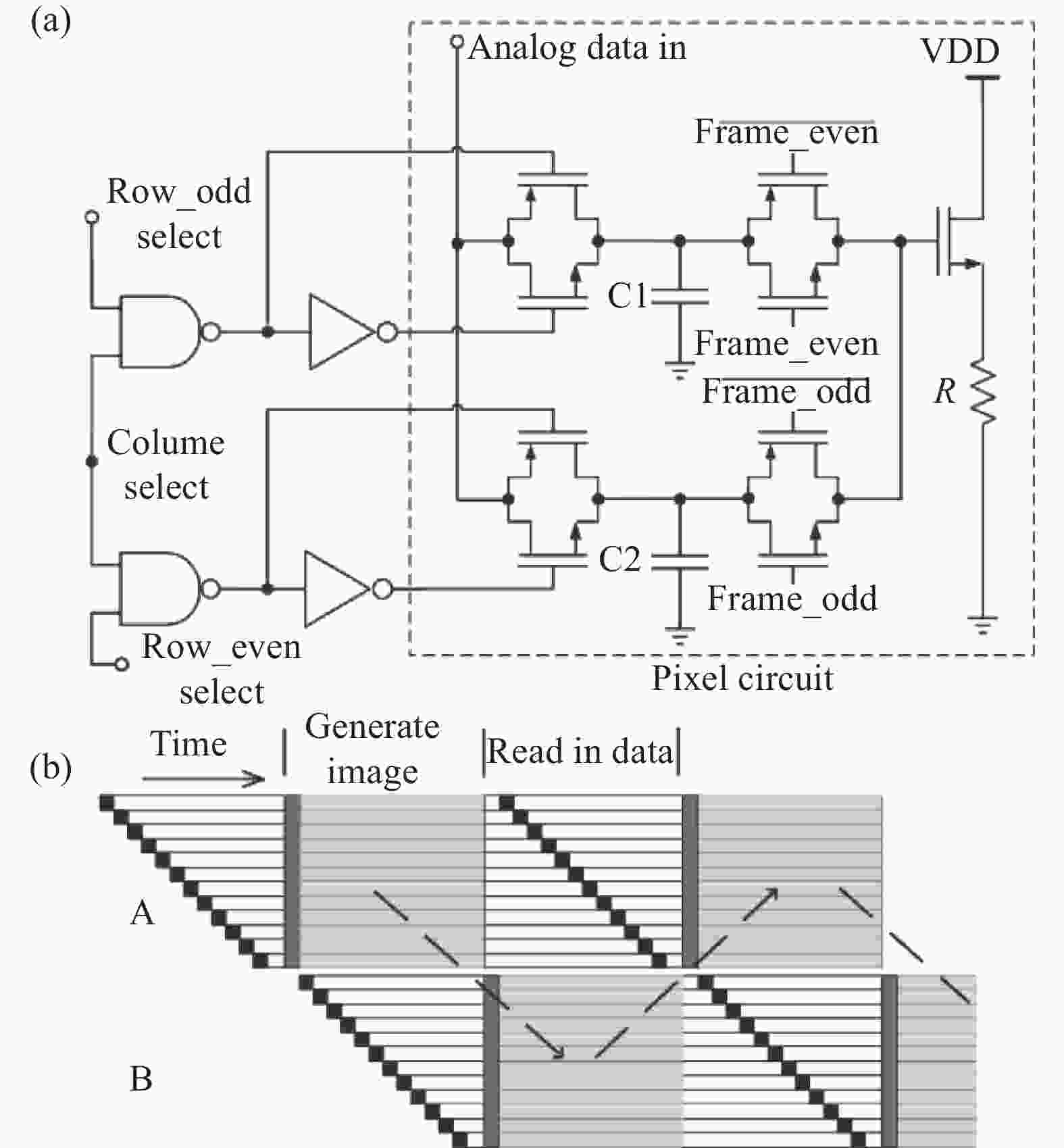
图 2 (a)电阻阵像素驱动电路;(b)快闪模式与扫描模式结合时序图
Figure 2. (a) Pixel drive circuit of resistor array device; (b) Work flow of snap shot mode and scanning mode
微辐射元内电阻R由一个MOS管驱动,形成源跟随放大器结构。其输出与栅极输入的关系为:
$$ \begin{array}{c}{V}_{R}=\dfrac{1}{2}{K}_{N}\dfrac{W}{L}{\left({V}_{G}-{V}_{R}-{V}_{TH}\right)}^{2}\end{array} $$ (1) 式中:VR为微辐射元两端的电压;KN为MOS驱动管的增益因子;VTH为MOS驱动管的阈值电压。源跟随器增益为:
$$ \begin{array}{c}\dfrac{\partial {V}_{R}}{\partial {V}_{\rm in}}=\dfrac{{g}_{m}R}{1+\left(1+\eta \right){g}_{m}R}\end{array} $$ (2) 式中:gm为MOS驱动管的跨导;η为体效应引起的跨导因子。gmR足够大时,增益接近于1,VR几乎跟随VG变化,如图3所示。最大驱动效率在不同的CMOS制造工艺以及不同MOS管尺寸下会有较大差异。
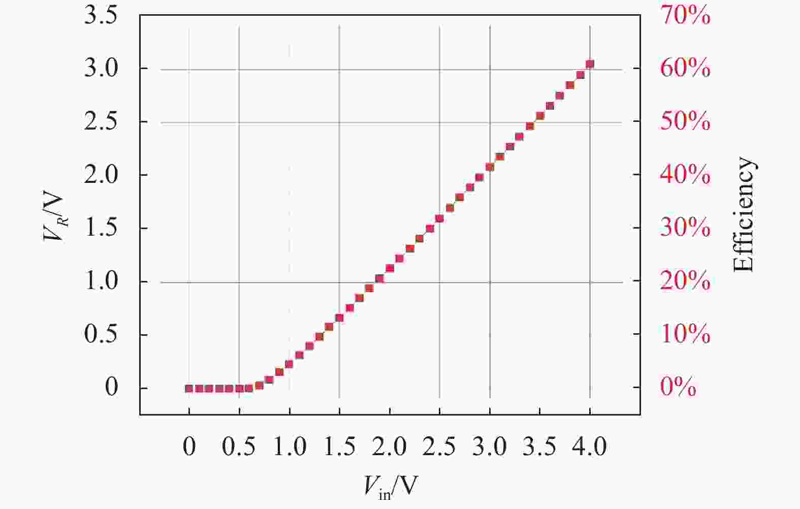
图 3 微辐射元电压VR和MOS管驱动效率随栅输入电压Vin的变化
Figure 3. Micro emitter voltage VR & MOS tube driving efficiency vs. grating input voltage Vin
MOS管控制电压VG由信号电压VS和偏置电压Vbias共同组成,而VS由图像数字信号经DAC转换形成。合理设置Vbias的情况下,微辐射元的加热功率近似为:
$$ \begin{array}{c}{P}_{R}={V}_{S}^{2}/R\end{array} $$ (3) 考虑电阻的非均匀性和温度系数,有:
$$ \begin{array}{c}{P}_{R}=\dfrac{{V}_{S}^{2}}{{R}_{0}\left(1+\gamma \right)\left(1+\alpha T\right)}\end{array} $$ (4) 式中:γ为非均匀性系数;α为电阻温度系数。电阻的γ和α的实际存在,以及加热功率与电压的平方关系,使得驱动电压输入与辐射功率输出之间的关系具有较强非线性特性。辐射图像灰度分辨率的控制也将具有较强非线性特性,其由DAC的分辨率和R的大小共同决定。
微辐射元阵列的总功耗为:
$$ \begin{array}{c}{P}_{Array}={\sum }_{m,n}{P}_{m,n}\end{array} $$ (5) 此外,由图3可知:MOS管驱动效率小于1,其本身也会产生一部分热量。系统散热能力决定了微辐射元阵列的总功耗上限,限制了图像的最高最低红外表观温度。以驱动效率等于60%为例,以0.6 mW驱动微辐射元,像素总功耗为1 mW,满功率运转的极限条件下1024×1024阵列总功耗为1 kW,在大多数应用场景中电阻阵大部分时间工作于极限功率的一半以下,散热条件较容易满足。为了保持大规模电阻阵列的正常运转,微辐射元功率应限制在0.6 mW以下。
-
像素电路和MEMS电阻共同组成一个像素,其集成方式主要有两种技术方案。一种方案是将像素电路与MEMS电阻设置在一个平面内,像素电路与MEMS电阻通过水平金属线连接,MEMS结构则通过腐蚀硅衬底形成。目前国内自研的256×256及512×512电阻阵均采用了这种方案[8-9],但这种方案的MEMS微辐射元占空比低,在进一步扩大器件规模方面面临诸多困难和限制。另一种技术方案是在像素电路上方垂直集成MEMS电阻,其结构和剖面示意如图4所示。

图 4 微辐射元垂直集成结构(a)和截面示意(b)
Figure 4. Vertically integrated structure (a) and sectional drawing (b) of the micro emitter
与非制冷焦平面不同的是,虽然都是在像素电路上集成MEMS结构,但电阻阵作为一种功率型高温辐射器件,其像素电流的大小比非制冷焦平面高一个量级以上。因此,MEMS电阻与像素电路之间可靠的垂直电学连接非常重要。在电阻阵MEMS结构设计上,采用了两端金属柱与CMOS电路的顶层金属连接的方案,将电阻阵复合薄膜结构悬置于电路之上形成高架式“微桥”结构。两端金属柱既起到力学支撑作用,也起到电学连接作用。金属柱与衬底的接触面积设计为8 μm×8 μm,较大的面积保证了微辐射元与衬底金属的良好电连接。微桥细长的桥腿则起到热隔离作用,宽度为2~4 μm,需根据仿真结果辅助设计最优值。器件在工作时,微桥中部大块区域为主要红外辐射面。辐射面内部的S型电阻阻值较大,通过桥腿内的阻值较小的电极与金属柱连接。由于MEMS电阻直接架设在像素电路之上,器件的占空比得到了大幅提升。在像素大小46 μm × 46 μm情况下,器件的占空比可达到51%。
微桥的主要结构材料采用氮化硅薄膜。氮化硅薄膜不仅耐高温,残余应力的工艺控制也较简单,杨氏模量较大,加工过程中和工作过程中均不易发生形变。同时,氮化硅还具有热导系数较低、长波红外辐射率高等优点。电极材料可采用热导率相对较低的钛。电阻材料可采用金属铂或镍铬薄膜,兼顾耐高温和低电阻温度系数的要求。碳化硅等薄膜的加入可起到MEMS红外辐射特性的调控作用。
真空中工作的电阻阵微辐射元温升可用以下的热平衡方程描述:
$$ \begin{array}{c}C\dfrac{{\rm{d}}T}{{\rm{d}}t}+{G}_{L}\left(T-{T}_{S}\right)+A\varepsilon \sigma \left({T}^{4}-{{T}_{0}}^{4}\right)=P\end{array} $$ (6) 式中:等式左侧三项分别为微桥自身的温度变化所消耗的功率、细长桥腿的热传导引起的功率和热辐射引起的功率;P为电学加热功率;C为微桥的比热容;GL为桥腿的热导;T为桥面平均温度;TS为衬底温度;A为桥面的面积;ε为微桥表面发射率;σ为斯忒藩-玻耳兹曼常数,其值为5.7×10⁻⁸ W/(m2·K4);T0为环境温度。
由于电阻阵通常工作于真空环境中,空气热对流和热传导均可忽略。辐射功率占比通常在5%以下,计算物理温度变化时可忽略该项。公式(6)的升温解和降温解表达式分别为公式(7)和公式(8):
$$ \begin{array}{c}\Delta T=\dfrac{P}{{G}_{L}}\left(1-{\rm e}^{-{G}_{L}t/C}\right)\end{array} $$ (7) $$ \begin{array}{c}\Delta T=\dfrac{P}{{G}_{L}}{\rm e}^{-{G}_{L}t/C}\end{array} $$ (8) 式中:ΔT为t时刻辐射面温度T与衬底温度TS的差,服从指数函数分布,特征时间为τ=C/GL。温度改变量在10%~90%之间经历的时间称为热响应时间,约为tresponse=2.4τ,决定了微辐射元可工作的最大帧频。
物理温升最大值为P/GL,P决定于CMOS电路的设计。微辐射元的最高温度决定了红外辐射量。辐射与波长λ、温度T的关系可以用普朗克公式表示:
$$ \begin{array}{c}{B}_{b}\left(\lambda ,T\right)=\dfrac{{c}_{1}{\lambda }^{-5}}{{\exp}\left(\dfrac{{c}_{2}}{\lambda T}\right)-1}\end{array} $$ (9) 其中
$$ {c}_{1}=2\pi h{c}^{2}=3.74\times {10}^{-16}\;{{\rm{W{\cdot}m}}}^{2} $$ $$ {c}_{2}=\frac{hc}{k}=1.44\times {10}^{-2}\;{\rm{m{\cdot}K}} $$ 对于红外探测系统来说,电阻阵红外图像的红外表观温度(等效黑体温度)是像素内所有红外辐射通量综合的平均等效值。假设MEMS微桥的平均温度为T,衬底的平均温度为Ts,电阻阵像素在λ1~λ2波段内的辐射能量可用公式(10)表达,单位为W·sr-1。等式右侧第一项为MEMS微辐射元的辐射功率,第二项为衬底的辐射功率。
$$ \begin{split} {P}_{IR}=&{\displaystyle\int }_{{\lambda }_{1}}^{{\lambda }_{2}}A\cdot {B}_{b}\left(\lambda ,{T}_{eff}\right){\rm{d}}\lambda =\\ &{\displaystyle\int }_{{\lambda }_{1}}^{{\lambda }_{2}}A\cdot {{F F\cdot \varepsilon }_{1}\left(\lambda \right)\cdot B}_{b}\left(\lambda ,T\right){\rm{d}}\lambda +\\ &{\displaystyle\int }_{{\mathrm{\lambda }}_{1}}^{{\mathrm{\lambda }}_{2}}{A\cdot \left(1-{F F}\right)\cdot {\varepsilon }_{0}\left(\lambda \right)\cdot B}_{b}\left({\lambda ,T}_{S}\right)\mathrm{d}\mathrm{\lambda } \end{split}$$ (10) 式中:Teff为像素单元的红外表观温度;A为像素单元面积;FF为微桥占空比;ε1和ε0分别为微桥和衬底的红外发射率。
由公式(10)可知,电阻阵的最低辐射功率取决于衬底温度TS。高温下辐射功率主要取决于第一项,与微桥占空比FF和微桥表面发射率ε1直接成比例关系。
由上面的分析可知,决定电阻阵红外辐射特性的关键因素有MEMS微辐射元的占空比、比热容、热导和表面发射率等。在达到同样等效黑体温度的情况下,高占空比像素设计可以显著缓解MEMS微桥的温升压力。通过MEMS微桥结构设计的优化,可以使电阻阵的像素功率、占空比、温升、辐射波段等特性达到最优化的平衡,同时,这种垂直集成的电阻阵MEMS设计在规模上具有较强的可扩展性。
-
热平衡下,电阻阵微桥的红外吸收率等于红外发射率。设计上可通过增强吸收的设计方法增强发射。通过调整厚度变量组(d1,d2,d3,h)以及增加衬底表面反射层,可形成特定波段高吸收的光学谐振腔。衬底表面反射层可通过CMOS电路的金属走线布局实现。采用(d1, d2, d3, h) = (100 nm, 400 nm, 500 nm, 1700 nm)的厚度设计,根据各层薄膜的折射率(n)和消光系数(k)的测试数据,利用光学薄膜特征矩阵法计算得到其在4~14 μm的表面吸收率、透过率和反射率,如图5所示。其在4~5 μm中波红外和8~12 μm长波红外波段的平均表面发射率分别达到0.7和0.8。碳化硅在4~5 μm中波红外波段消光系数较大,使得微辐射元的中波红外表面发射率有明显提升,由此实现了双波段均具有高表面发射率的设计。若想在不增加厚度情况下达到更高发射率,则需应用在中长波红外波段拥有更高消光系数的薄膜。

图 5 SiC和SiNx薄膜的折射率(n)(a)和消光系数(k)(b)数据;包含、不包含SiC薄膜的微辐射元红外光学特性仿真结果(c)
Figure 5. Refractive index (n) (a) and extinction coefficient (k) (b) of SiNx and SiC films; Infrared optical characteristic simulation of micro emitter with and without SiC film (c)
-
通过热力学仿真,获得了不同功率下微辐射元的物理温度、热响应时间、红外表观温度和形变等工作特性,建立图像数据输入到红外辐射输出的函数关系。表1为仿真所用材料的各项参数。
表 1 微辐射元仿真参数
Table 1. Parameters of micro emitter used in simulation
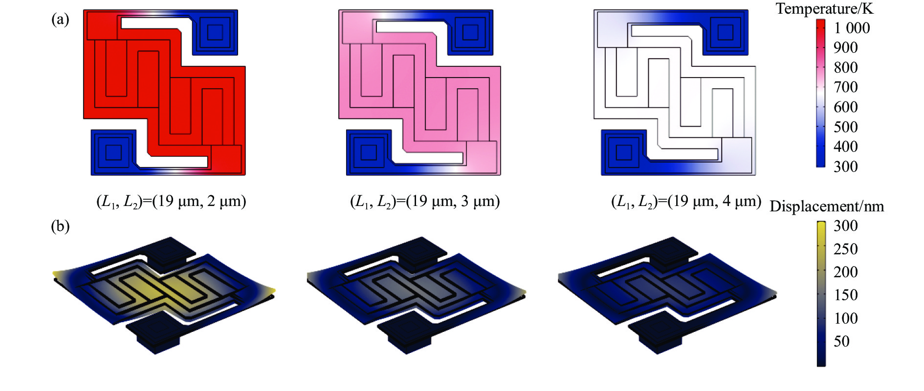
Parameters SiNx SiC Ti Constant pressure heat capacity/J·kg−1·K−1 690 680.7 522 Material density/kg·m−3 3000 2979 4506 Thermal conductivity/W·m−1·K−1 3.25 116.6 21.13 Young’s modulus/GPa 270 400 115.7 Poison ratio 0.245 0.16 0.321 Coefficient of thermal expansion/K−1 0.8e-6 2.7e-6 8.6e-6 图6显示了不同桥腿形状的微辐射元在0.6 mW功率驱动下的热平衡温度分布特性和力学特性。两端金属柱所接触衬底温度为20 ℃。可见不同功率下桥面温度分布均匀,温差不超10 ℃,绝大部分温差落在两侧桥腿上。由仿真可见,低应力氮化硅的应用使得微辐射元的形变量极小,主要为翘曲,最大位移量小于300 nm,平行于衬底面的位移量极小,可忽略不计,表明占空比仍有提升空间。高频状态下工作时,桥体会反复形变积累动能,小形变量有助于延长器件的寿命,同时避免辐射面与其他部分接触形成热短路导致辐射能量大幅下降。

图 6 0.6 mW功率下微辐射元的温度分布(a)和形变(b)仿真结果
Figure 6. Temperature distribution (a) and displacement (b) simulation results of micro emitter under 0.6 mW
在同样的功率驱动下,不同长度组设计的微辐射元的热导、热容、热响应时间以及中波和长波红外表观温度的仿真结算结果如表2所示。可见三种设计均能满足红外表观温度的性能要求,L2=2 μm时,中波红外和长波红外表观温度分别超过了800 K和700 K,但牺牲了热响应速度,热响应时间超过了5 ms。L2=4 μm时,热响应时间不足2 ms,但红外表观温度较小。取中间值L2=3 μm作为最终的结构设计,满足性能要求的同时拥有较好的容错率。
表 2 微辐射元的热属性与性能
Table 2. Heat properties and performance of micro emitter
Item Length/μm (L1,L2) =(19,2) (L1,L2) =(19,3) (L1,L2) =(19,4) C/×10−9 J·K−1 2.24 2.23 2.22 GL/×10−6 W·K−1 0.8 1.2 1.6 tresponse/ms 5.59 3.91 1.97 MWIR Teff/K 832 658 565 LWIR Teff/K 725 582 505 取桥腿宽度为3 μm,根据公式(9)可计算得到像元在不同功率下的红外表观温度,仿真结果如图7所示。驱动功率与红外表观温度成近线性关系,0.6 mW功率驱动下,像素最高中波红外表观温度可达658 K,最高长波红外表观温度可达582 K,均超过了目前在用的国产电阻阵器件所能达到的红外表观温度[7-8]。图7中间子图是红外辐射亮度与控制电压关系的仿真结果。辐射亮度的控制特性直接反映了红外图像的灰度控制性能。由电压驱动MOS管电流,电流使电阻温度变化,继而反映到辐射亮度的变化,该过程中的多个转换使得控制曲线具有较明显的非线性。以采用12 bit DAC输出为例,明显可见在低等级段辐射亮度分辨率较高,而高等级段分辨率较低,且在中波红外波段非线性更强,这对于图像灰度控制和非均匀性校正来说均是一个挑战。由于文中所设计的像素CMOS驱动电路的功能简单,为阵列外围驱动电路的设计留下了很大的设计空间,在设计芯片时可考虑在片上直接集成现场非线性校正电路。热响应特性的仿真结果显示,不同功率驱动下的升降温热响应时间几乎无区别,均小于5 ms,微辐射元可工作于200 Hz以上。

图 7 性能仿真结果。(a)表观温度与功率关系;(b)辐射亮度与电压控制关系;(c)热响应曲线
Figure 7. Performance simulation results. (a) Apparent temperature vs power; (b) Radiance vs voltage control code; (c) Heat response curve
-
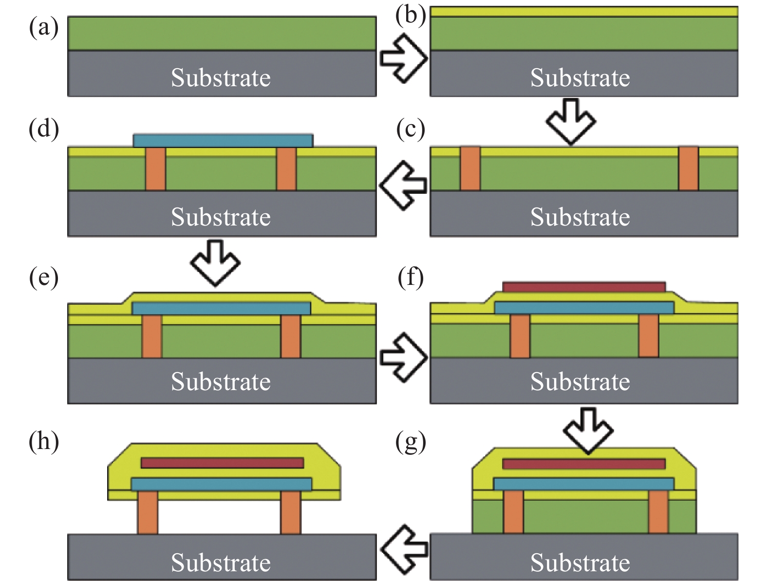
采用在CMOS晶圆上方继续加工,垂直集成MEMS工艺的方案。MEMS工艺与CMOS集成电路制造工艺分离,可对芯片设计和微辐射元阵列设计分别验证,降低试错成本。微辐射元阵列制备工艺流程如图8所示,依次为:牺牲层制备(图8(a));氮化硅薄膜沉积(图8(b));金属柱制备(图8(c));电学薄膜沉积与图形化(图8(d));氮化硅薄膜沉积(图8(e));碳化硅薄膜沉积与图形化(图8(f));氮化硅薄膜沉积与微桥形状刻蚀(图8(g));牺牲层去除(图8(h))。
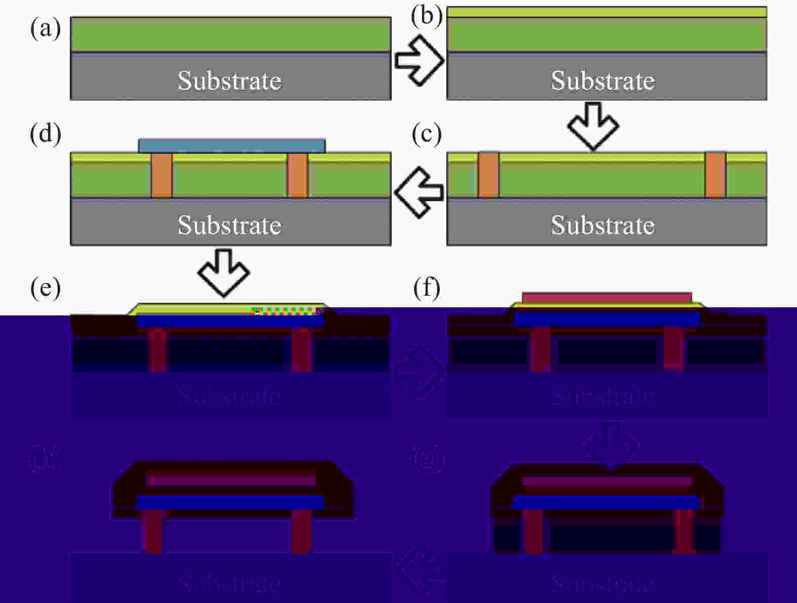
图 8 MEMS工艺流程图
Figure 8. MEMS process flow
-
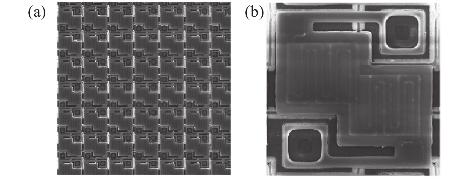
设计了640×410微辐射元阵列,在带有金属网络的8 in(1 in=2.54 cm)晶圆上进行了MEMS工艺流片实验。图9为微辐射元阵列的微观图像,图中单元结构清晰可见,图形均匀,在去除牺牲层后,金属柱与桥腿可支撑桥面,且无明显形变,与预测一致。证明MEMS工艺方案可行且一致性良好。

图 9 640×410微辐射阵列样品的SEM显微图
Figure 9. SEM micrograph of 640×410 micro emitter array sample
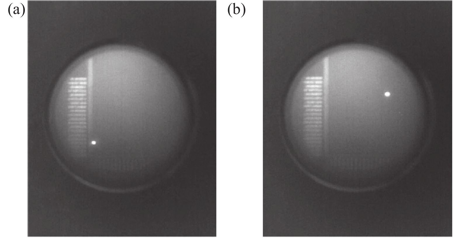
阵列样品下方金属网络的设计可对阵列进行抽样点亮,图10为阵列样品的角落区域与中间区域的4×1 pixel在空气中驱动的长波红外图像,结果显示电学连接正常,微辐射元可正常驱动。在驱动加热功率0.6 mW条件下,空气中像素在8~12 μm波段的表观温度约为400 K。考虑到大气环境和真空环境中像素热导相差约有3倍,测试结果与设计仿真结果基本相符。严格的性能测试需要集成CMOS电路并将阵列进行真空封装方可进行。初步测试结果证明了设计的可行性。

图 10 640×410阵列样品的角落(a)与中间(b)处的4×1 pixel在空气中驱动的长波红外图像
Figure 10. LWIR image of 4×1 pixel driving in the air at the corner (a) and center (b) of a 640×410 array sample
-
针对大规模高辐射效率电阻阵红外景象产生器的研制设计需求,提出了CMOS像素驱动电路与高占空比微辐射元阵列一体化的设计方案。驱动电路兼容扫描模式和快闪模式。微辐射元占空比达51%。设计仿真表明,在0.6 mW功率驱动下,热响应时间小于5 ms,阵列像元的最高中波红外表观温度达658 K,最高长波红外表观温度达582 K,应力翘曲小于300 nm。提出了完整的MEMS工艺制备方案,通过小阵列流片验证了制备方案可行性,并通过初步测试验证了样品的功能完整性。该设计实现了高辐射效率和强可拓展性,为大规模电阻阵的研制指明了方向。
Pixel design of large-scale resistor array infrared scene projector
-
摘要: 电阻阵作为一种动态红外景象产生器件,在红外半实物仿真领域有着重要的应用。电阻阵可实现的规模与性能与红外微辐射像素列阵的设计有着密切的关系。文中从应用系统对大规模电阻阵器件的要求出发,结合电阻阵的工作原理,提出了像素驱动电路与MEMS结构一体化的设计方案,设计了规模可拓展的高占空比像素结构。通过采用高消光系数材料以及光学谐振腔结构,微辐射元的中波红外和长波红外的表面发射率达0.7。热力学仿真表明,通过合理的薄膜厚度和结构设计,微辐射元阵列的占空比达到51%,升、降温的热响应时间均小于5 ms,0.6 mW功率驱动下应力翘曲小于300 nm,长波红外表观温度可达582 K,中波红外表观温度可达658 K。结合设计方案提出了工艺制备方案,并通过小阵列流片初步验证了设计方案的可行性。该设计研究为国产大规模、高占空比电阻阵的研制指明了方向。Abstract:
Objective As an infrared scene projector, the resistor array device played an important role in hardware-in-the-loop infrared simulation system. Due to the emitted infrared image similar to the real target, it can generate dynamic infrared scene for infrared detectors. Usually, the scale of the infrared detector was 512 × 512 or 640 × 480, meaning the scale of the target simulator should be four times larger to ensure high-quality simulations, and developing a 1 024 × 1 024 scale resistor array device is necessary. The pixel design is the basis of resistor array and it determines the achievable scale and performance of the resistor array. Therefore, a pixel array that can be scalable to 1 024 × 1 024, can operate at 200 Hz, and has an apparent temperature close to 600 K must be achieved. For this purpose, a design scheme for integrating the pixel driving circuit and MEMS structure was proposed, and a scalable high-fill-factor pixel was designed in this paper. Methods A pixel circuit operating in snapshot mode was designed according to the functional requirements of the resistor array device (Fig.2). By investigating the design scheme for integrating the pixel driving circuit and MEMS structure, four key factors influencing the pixel performance were deduced, including fill factor, thermal conductance, heat capacity, and surface emissivity. Using the high extinction coefficient materials and an optical resonator structure, the surface emissivity of the micro emitter in mid-wave infrared and long-wave infrared reaches 0.7 (Fig.5). Through proper film thickness design and geometric structure design, the fill factor of the micro emitter array reaches 51% (Fig.4). The thermodynamic simulation was used to assist the design of the micro emitter and evaluate its performance (Fig.6). A MEMS fabrication process was proposed to prepare pixel array sample (Fig.8). Results and Discussions The thermodynamic simulation results of the designed pixel show that the apparent temperature of mid-wave infrared and long-wave infrared at 0.6 mW power drive reaches 658 K and 582 K, respectively (Fig.7). The thermal response time for both heating and cooling is less than 5 ms, meaning the pixel can work at 200 Hz. The displacement of the emitter is less than 300 nm, which benefited from the geometry structure and the materials applied. The 640 × 410 array sample showed excellent geometry uniformity (Fig.9). The sample pixel was tested in air at 0.6 mW power drive and showed a long-wave infrared apparent temperature of about 400 K. The image result of this sample proved that the pixel design was achievable and functional (Fig.10). Conclusions Aiming at the requirements of developing large-scale resistor array devices, a design scheme for integrating the CMOS driving circuit and the MEMS structure into the pixel was proposed. The pixel driving circuit can work in snapshot mode. Benefiting from the MEMS structure, the fill factor of the micro emitter reaches 51%, which is much higher than that of the traditional resistor array. The thermodynamic simulation results showed that the radiation efficiency of the designed pixel was sufficiently high and capable of being applied in 1 024 × 1 024 resistor array device design. An array sample was fabricated using the proposed MEMS process. The test result of this sample proved the pixel design is achievable. The design research indicates the direction for developing domestic large-scale and high-fill-factor resistor array devices. -
Key words:
- resistor array /
- infrared simulation /
- micro emitter /
- infrared apparent temperature /
- fill factor
-
图 1 (a)电阻阵结构框图;(b)红外图像产生示意图
Figure 1. (a) Block diagram of the resistor array structure; (b) Schematic of infrared image generation
图 2 (a)电阻阵像素驱动电路;(b)快闪模式与扫描模式结合时序图
Figure 2. (a) Pixel drive circuit of resistor array device; (b) Work flow of snap shot mode and scanning mode
图 3 微辐射元电压VR和MOS管驱动效率随栅输入电压Vin的变化
Figure 3. Micro emitter voltage VR & MOS tube driving efficiency vs. grating input voltage Vin
图 4 微辐射元垂直集成结构(a)和截面示意(b)
Figure 4. Vertically integrated structure (a) and sectional drawing (b) of the micro emitter
图 5 SiC和SiNx薄膜的折射率(n)(a)和消光系数(k)(b)数据;包含、不包含SiC薄膜的微辐射元红外光学特性仿真结果(c)
Figure 5. Refractive index (n) (a) and extinction coefficient (k) (b) of SiNx and SiC films; Infrared optical characteristic simulation of micro emitter with and without SiC film (c)
图 6 0.6 mW功率下微辐射元的温度分布(a)和形变(b)仿真结果
Figure 6. Temperature distribution (a) and displacement (b) simulation results of micro emitter under 0.6 mW
图 7 性能仿真结果。(a)表观温度与功率关系;(b)辐射亮度与电压控制关系;(c)热响应曲线
Figure 7. Performance simulation results. (a) Apparent temperature vs power; (b) Radiance vs voltage control code; (c) Heat response curve
图 9 640×410微辐射阵列样品的SEM显微图
Figure 9. SEM micrograph of 640×410 micro emitter array sample
图 10 640×410阵列样品的角落(a)与中间(b)处的4×1 pixel在空气中驱动的长波红外图像
Figure 10. LWIR image of 4×1 pixel driving in the air at the corner (a) and center (b) of a 640×410 array sample
表 1 微辐射元仿真参数
Table 1. Parameters of micro emitter used in simulation
Parameters SiNx SiC Ti Constant pressure heat capacity/J·kg−1·K−1 690 680.7 522 Material density/kg·m−3 3000 2979 4506 Thermal conductivity/W·m−1·K−1 3.25 116.6 21.13 Young’s modulus/GPa 270 400 115.7 Poison ratio 0.245 0.16 0.321 Coefficient of thermal expansion/K−1 0.8e-6 2.7e-6 8.6e-6  下载: 导出CSV
表 2 微辐射元的热属性与性能
Table 2. Heat properties and performance of micro emitter
Item Length/μm (L1,L2) =(19,2) (L1,L2) =(19,3) (L1,L2) =(19,4) C/×10−9 J·K−1 2.24 2.23 2.22 GL/×10−6 W·K−1 0.8 1.2 1.6 tresponse/ms 5.59 3.91 1.97 MWIR Teff/K 832 658 565 LWIR Teff/K 725 582 505
下载: 导出CSV
-
[1] 吴根水, 屠宁, 赵松庆, 等. 红外成像制导空空导弹半实物仿真技术研究[J]. 航空科学技术, 2011 (3): 58-61. doi: 10.3969/j.issn.1007-5453.2011.03.018 Wu Genshui, Tu Ning, Zhao Songqing, et al. Research of infrared imaging guide Hardware-in-the-Loop(HWIL) simu-lation technology [J]. Aeronautical Science & Technology, 2011(3): 58-61. (in Chinese) doi: 10.3969/j.issn.1007-5453.2011.03.018 [2] Tang S, Song M, Wang B, et al. Infrared scene generation technology based on hardware-in-the-loop simulation of MOS resistance arrays [J]. Journal of System Simulation, 2018, 30(4): 1319. (in Chinese) doi: 10.16182/j.issn1004731x.joss.201804014 [3] Hao Yanyun, Zhao Songqing. Overview of hardware-in-the-loop infrared multi-band target simulation technologies abroad [J]. Infrared, 2022, 43(2): 7-14, 43. (in Chinese) doi: 10.3969/j.issn.1672-8785.2022.02.002 [4] Song Minmin, He Chongyu, Ji Yaping, et al. Simulation technology of medium and long wave dual color target and jamming [J]. Infrared and Laser Engineering, 2022, 51(3): 20210208. (in Chinese) doi: 10.3788/IRLA20210208 [5] Wang Yunping, Zhao Changming. Dynamic infrared scene simulation system based on the digital micro-mirror device [J]. Infrared and Laser Engineering, 2009, 38(6): 966-970. (in Chinese) [6] Xu Jialin, Wang Xiaodong, Li Bingyu, et al. Method to transfer and store image data of infrared scene projector based on DMD [J]. Infrared and Laser Engineering, 2015, 44(9): 2622-2626. (in Chinese) [7] Zhang Kai, Ma Bin, Huang Yong, et al. Method of 256-resolution resistor array performance testing and non-linearity correction [J]. Infrared and Laser Engineering, 2012, 41(11): 2921-2926. (in Chinese) [8] 马斌, 张凯, 高蒙, 等. 256×256高帧频及128×128高占空比电阻阵列的性能测试结果[C]//全国光电技术学术交流会, 2012. [9] Ma Bin, Cheng Zhengxi, Zhai Houming, et al. Development of domestic resistive arrays technology [J]. Infrared and Laser Engineering, 2011, 40(12): 2314-2322. (in Chinese) [10] Cheng Zhengxi, Ma Bin, Liu Qiang, et al. 128×128 resistor array with suspended micro-bridge fabricated through film transfer process [J]. Infrared and Laser Engineering, 2012, 41(3): 559-562. (in Chinese) [11] Oleson J, James J, LaVeigne J, et al. Large format resistive array (LFRA) infrared scene projector (IRSP) performance and production status[C]//Technologies for Synthetic Environments: Hardware-in-the-Loop Testing XII. SPIE, 2007, 6544: 29-38. [12] Sparkman K, LaVeigne J, McHugh S, et al. Scalable emitter array development for infrared scene projector systems[C]//Infrared Imaging Systems: Design, Analysis, Modeling, and Testing XXV. SPIE, 2014, 9071: 492-498. [13] Danielson T, Franks G, Holmes N, et al. Achieving ultra-high temperatures with a resistive emitter array[C]//Infrared Imaging Systems: Design, Analysis, Modeling, and Testing XXVII. SPIE, 2016, 9820: 240-248. [14] Hao Yanyun, Zhao Songqing, Wu Genshui, et al. Dynamic image frame frequency testing method of MOS resistor array IR target simulator [J]. Computer Measurement & Control, 2018, 26(2): 17-20. (in Chinese) doi: 10.16526/j.cnki.114726/tp.2018.02.005 -

 点击查看大图

计量
- 文章访问数: 129
- HTML全文浏览量: 47
- PDF下载量: 79
- 被引次数: 0

