


-
光电成像系统采用光学系统接收到目标场景的光辐射,并通过成像探测器光电转换作用完成目标场景图像的获取[1]。相对其他成像体制,光电成像系统以其体积小、质量轻、可靠性高、分辨率高以及动态范围大等优势,被广泛应用于医疗成像、影像传媒、安防管理、目标高分辨侦察识别、光电精确制导、火控和瞄准、飞行辅助等领域[2]。光电成像系统为获得清晰图像,通常引入自动对焦机制,可使面阵光电探测器与成像目标始终关于光学系统共轭,该机制会造成入射目标光能量全部汇聚到焦平面探测器表面,形成很大的光学增益。当有强激光进入光学系统后,因为光学系统高增益的存在,探测器极易被干扰甚至损伤[3-4]。近年来,随着激光器功率/能量水平的大幅提升,激光武器装备日益增多,针对光电成像系统的激光致盲和激光致眩现象频发[2]。激光入射到光电成像系统探测器靶面的功率/能量密度不同造成的干扰效果可分为致盲和致眩。激光致盲主要是指激光对光电系统中的探测器造成永久性损伤,使之失去传感或者成像能力[5]。激光致眩是致盲概念的拓展,指激光使干扰对象暂时性失去正常的传感能力或者成像能力[5]。通常,同一光电成像系统致盲干扰所需的到靶功率/能量密度大于致眩干扰。光电成像系统采用防护技术后,到达探测器表面的功率/能量密度可能低于致盲阈值而高于致眩阈值,此时激光致眩防护仍然十分必要。同时,致眩干扰所需功率/能量密度低,因此,光电成像系统致眩防护现实需求更加广泛和迫切。面对日益严峻的激光威胁,如何有效提升光电成像系统的激光防护能力,确保光电成像探测器在强激光照射条件下能够不被损坏或干扰且能够正常成像是相关研究人员非常关心又亟待解决的问题,具有明确的应用需求和科学意义。
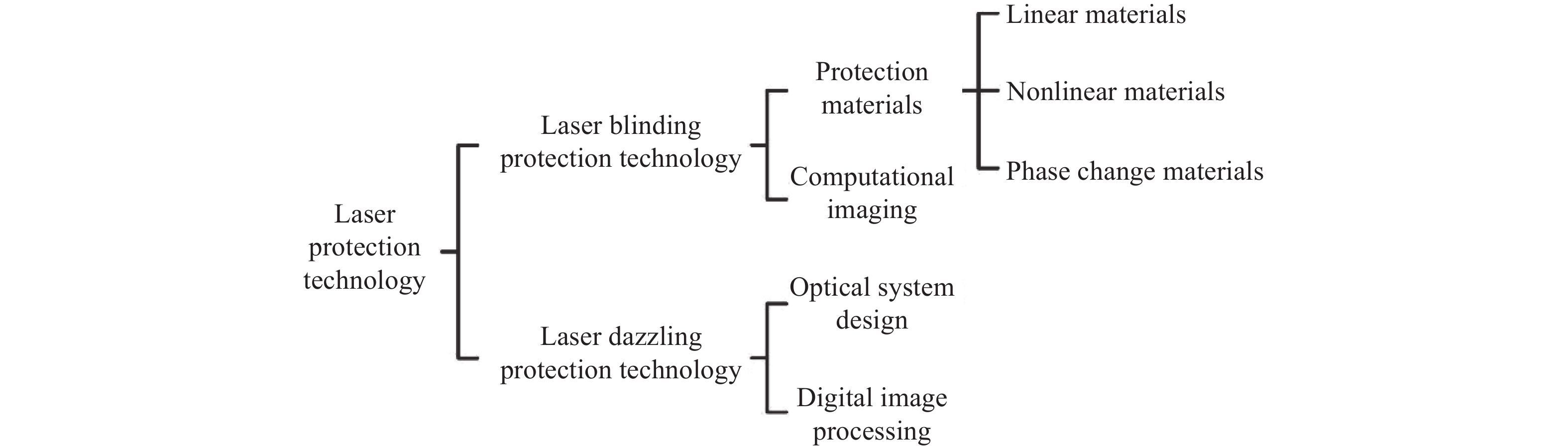
如图1所示,光电成像系统激光防护围绕激光致盲防护和激光致眩防护两大目标。光电成像系统激光致盲防护的技术主要包括采用防护材料和计算成像两类;光电成像系统激光致眩防护的技术主要包括光学系统设计和数字图像处理两类。

图 1 激光防护技术框图
Figure 1. Block diagram of laser protection technology
-
线性材料主要有选择吸收与选择反射等类型,针对某一特定波长的激光进行选择性的吸收和反射,截止相应波长的激光能量[6-7]。选择吸收技术利用材料自身的选择吸收特性,实现对特定波长激光的选择吸收来达到防护目的,该技术不受激光入射角度的影响,适用于较大视场的成像系统,且表面不易磨损,但是吸收能量易导致材料本身的损坏。选择反射技术通过多层介质膜结构的选择反射实现激光防护,反射能量能使材料承受更高强度的激光,但是反射效果受到激光入射角的影响,入射角达到45°时,多层介质膜结构丧失防护作用,且膜层结构的磨损会导致防护能力的下降甚至完全丧失[8]。部分研究尝试利用线性材料实现多波段的激光防护[9],但是并没有实质改善线性材料的窄防护带宽缺陷。此外,因为线性材料对光的强度极不敏感,因此无法实现同一波长强光时的高光学密度和弱光时的高透过率。
-
非线性材料[10]的特征为弱光照射时能量输出与输入呈线性关系,强光照射时产生非线性光学效应,输出能量被控制在一定范围内以达到激光致盲防护的效果。不同于线性材料,非线性材料的输出能量不仅与波长密切相关,还受光强的影响,激光能量超过防护阈值时材料开始限幅,激光能量超过损伤阈值时材料损伤失去限幅作用。非线性材料主要包括无机半导体纳米材料、共轭有机高分子、无机金属团簇化合物、碳纳米材料、及二维材料等五类[11]。非线性材料具有防护波段宽的优点,可以实现多波段激光和可调谐激光的防护,同时在较低光强情况下具有较高的透过率。但是,非线性材料存在材料溶解度低和液态基体实用性差的缺点,非线性材料的固态化,即实现固态基质中的有效均匀溶解是亟待解决的问题。近年来的研究热点在于石墨烯、过渡金属硫化物和黑磷等二维非线性光学材料的制备和应用测试[12]。
-
基于相变原理的防护材料可在外界激励作用下发生可逆相变,相变过程中材料的光学性质在极短时间内出现变化,利用相变前后光学性质差异实现激光防护作用。钒氧化物是研究较为广泛的用于激光防护的相变材料,其中二氧化钒(VO2)和五氧化二钒(V2O5)相变前后红外波段透射率变化显著[13]。1959年,贝尔实验室的Morin等[14]发现VO2材料在340 K温度激励下具有金属-绝缘相变(Metal-Insulator Transition,MIT)特性。VO2材料相变前后红外透过率的显著变化,使其成为红外波段重要的激光致盲防护材料。致盲激光攻击成像系统时,VO2材料在激光的激励作用下迅速发生相变转变为金属态,降低致盲激光的透过率,达到保护成像系统的目的。VO2材料在激光致盲防护方面的巨大潜力吸引研究人员围绕其机理探究、制备方法和应用研究开展相关研究。研究人员关注的防护技术指标包括防护带宽、光学密度、响应时间、防护阈值和损伤阈值等。
-
诱导VO2材料相变的方式包括光致相变、热致相变和电致相变等,其中光致相变和热致相变与激光防护密切相关。在探究相变机理[15]的相关研究中,相变响应时间定义为激光到达材料与材料开启防护作用的时间间隔,直接影响着VO2材料的激光防护性能,因此,研究人员对VO2材料的相变响应时间开展广泛研究,其中光致相变的响应时间相关研究如表1所示。
表 1 光致相变的响应时间相关研究
Table 1. Studies on response time of photoinduced transition
Sample property Synthesis method Test condition Response time Reference 32 nm-thick
VO2 thin filmLow-temperature process Pulse width: 450-550 fs
Energy density: 3.7 mJ/cm2
Wavelength: 780 nm<500 fs [16] 0.2 μm-thick
VO2 thin filmReaction evaporation deposition and annealing Biasing temperature: 52 ℃
Pulse width: 50 ns
Energy density: 150 mJ/cm2<50 ns [17] 0.2 μm-thick
VO2 thin film- Pulse width: 50 fs
Energy density: 7-25 mJ/cm2
Wavelength: 800 nm50 ps-100 fs [18] VO2-Si3N4 structures Chemically etching Pulse width: 100 fs
Energy density: 50 mJ/cm2
Wavelength: 790 nm<500 fs [19] VO2 microcrystals Vapour transport Pulse width: ~45 fs
Energy density: 3.3 mJ/cm2
Wavelength: 800 nmFemtosecond timescale [20] 25 nm-thick
VO2 thin filmPulsed laser deposition Pulse width: 4.9 fs
Pulse energy: ~100 mJ/cm2
Wavelength: 400-1000 nm(26±6) fs [21] 75 nm-thick
VO2 thin filmPulsed laser deposition and annealing Wavelength: 800 nm 200 fs [22] 1994年,Becker等[16]利用与聚合物基底相兼容的低温工艺制备厚度为32 nm的VO2薄膜,同时,采用波长780 nm的掺钛蓝宝石激光搭建飞秒和皮秒时间尺度的泵浦探针装置,泵浦激光能量密度为3.7 mJ/cm2时测定VO2的光致相变响应时间尺度小于500 fs。该研究证明VO2薄膜具有超快的相变响应时间,有望实现成像系统的激光防护。
1996年,查子忠等[17]利用反应蒸发沉积方法和退火处理镀制VO2薄膜。实验测得偏置温度为52 ℃、脉宽50 ns的TEA CO2激光能量密度为150 mJ/cm2时,VO2薄膜出现相变,响应时间<50 ns且恢复时间约为200 μs。
2001年,Cavalleri等[18]在玻璃基底上制备VO2薄膜,并利用泵浦探测技术测量薄膜的光致相变的响应时间,泵浦脉冲波长800 nm、脉宽50 fs、能量密度25 mJ/cm2情况下,测得薄膜的相变阈值为7 mJ/cm2,进一步通过实验数据的指数拟合发现,能量密度的增加导致相变时间从大于50 ps降低到约100 fs,如图2所示。

图 2 (a)泵浦脉冲的高斯空间轮廓; (b)相变过程中的反射率变化; (c)样品上三个不同位置的反射率的时间分辨演变,对应的能量密度为(c1) 7 mJ/cm2、(c2) 15 mJ/cm2和(c3) 25 mJ/cm2
Figure 2. (a) Gaussian spatial profile of pumping pulse; (b) Reflectivity during the phase transformation; (c) Time resolved evolutions of the reflectivity for three different positions on the sample, corresponding to local fluences of (c1) 7 mJ/cm2, (c2) 15 mJ/cm2, and (c3) 25 mJ/cm2
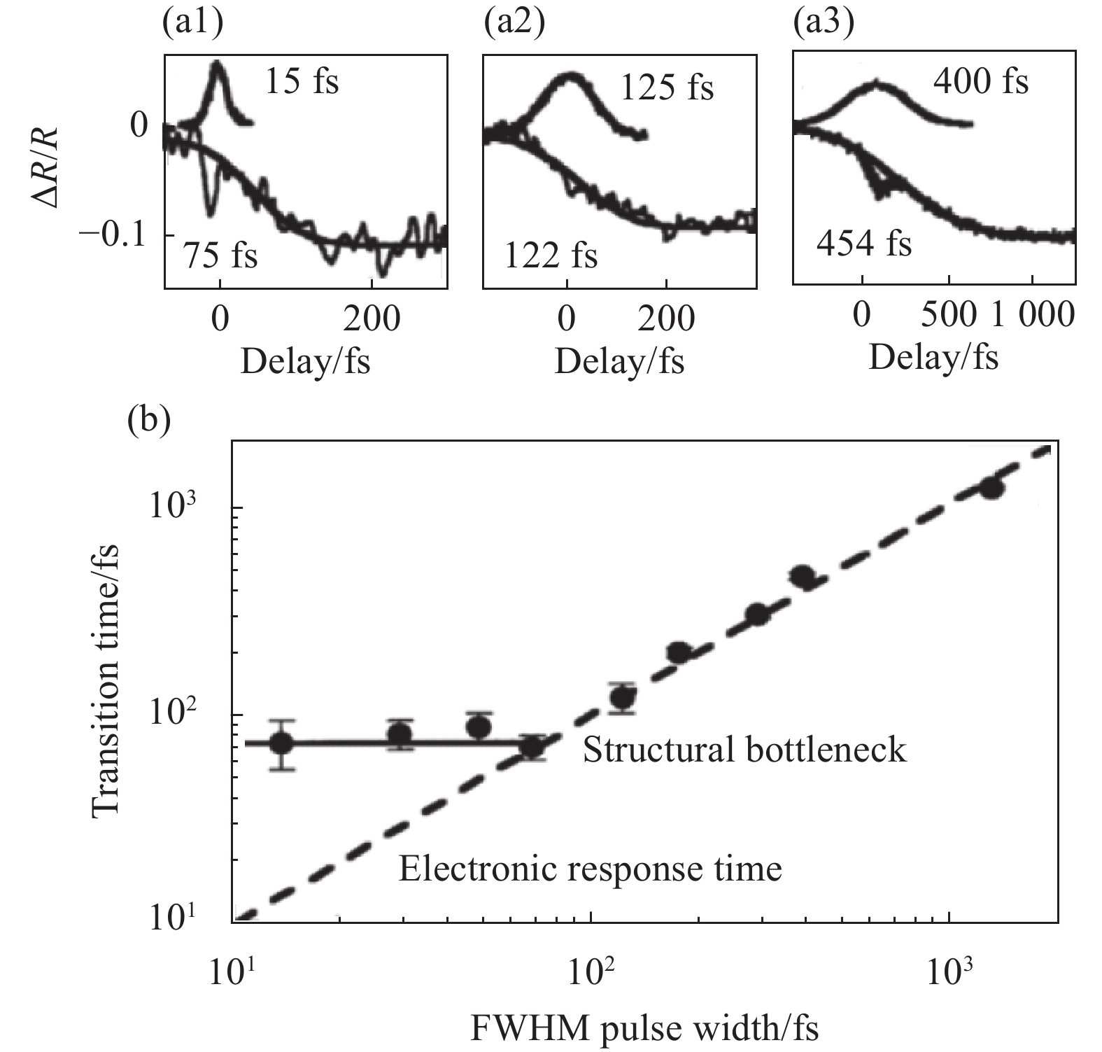
Cavalleri等[19]在进一步的研究实验中采用硅基底厚度(50±10) nm的VO2薄膜,以厚度(200±10) nm氮化硅(Si3N4)为缓冲层。利用化学刻蚀硅基底制备VO2-Si3N4结构,实验测量波长790 nm、脉宽100 fs、能量密度50 mJ/cm2的脉冲激光作用下VO2-Si3N4结构的反射率和透过率变化情况,可以估算该结构的相变响应时间小于500 fs。并研究泵浦脉宽在1.5 ps~15 fs之间变化时该薄膜的光致相变响应时间变化规律,结果如图3所示,观测到相变时间的80 fs为瓶颈。

图 3 光致相变的响应时间与脉宽的函数关系,脉宽位于1.5 ps~15 fs之间
Figure 3. Response time of photoinduced transition as a function of pulse width, which ranges from 1.5 ps to 15 fs
2015年,O'callahan等[20]采用气相输运方法[23]制备VO2微晶体,并通过频率分辨光学开关技术获取波长800 nm、脉宽~45 fs的激光脉冲,利用泵浦探测技术测量能量密度为3.3 mJ/cm2时相变响应时间与初始温度的关系,结果表明:初始温度升高会导致响应时间下降,且VO2微晶体的光致相变响应时间为飞秒量级。
2017年,Jager等[21]通过脉冲激光沉积法制备厚度25 nm的多晶VO2薄膜,利用泵浦探测技术测得该薄膜的光致相变响应时间为(26±6) fs,实验结果倾向于Mott-Hubbard机制。
2023年,Johnson等[22]采用脉冲激光沉积和退火工艺,在氮化硅膜上制备厚度75 nm的VO2薄膜,采用时间和光谱分辨共振软X射线相干成像技术观测VO2薄膜光致相变的动力学过程,测得相变时间为200 fs。
除光致相变外,激光还可能通过加热诱导VO2薄膜相变。1992年,Rana等[24]发现VO2薄膜在1.06 μm连续激光辐射下,激光加热诱导相变的响应时间为15~10 ms。
2006年,Wang等[25]研究VO2薄膜动态光学限幅性能时,发现在强度255 W/cm2、光斑直径2 mm的近红外连续激光照射下,VO2薄膜透过率相变前为47%,相变后下降到28%,激光加热诱导相变的响应时间为200 ms。
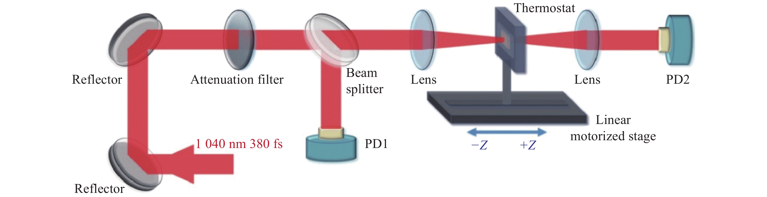
2022年,Wang等[26]利用可变温度Z扫描装置(图4)研究飞秒激光诱导VO2薄膜相变原理时,通过温度变化实验发现激光诱导的相变调制深度与环境温度诱导的相变的调制深度一致,且调制深度随着薄膜厚度线性增加,进一步证实相变是由高重复频率激光的热效应积累引起的。
综上所述,VO2材料的光致相变响应时间约为飞秒量级,热致相变响应时间约为毫秒量级。
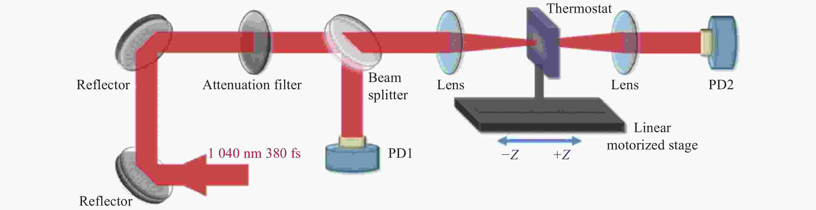
图 4 可变温度Z扫描装置的示意图
Figure 4. Schematic diagram of variable temperature Z-scan device
-
VO2薄膜的制备方法[27-28]多种多样,包括反应蒸发法、脉冲激光沉积法、粒子束溅射法和溶液法等等,研究人员通过优化参数改善VO2薄膜激光致盲防护性能。
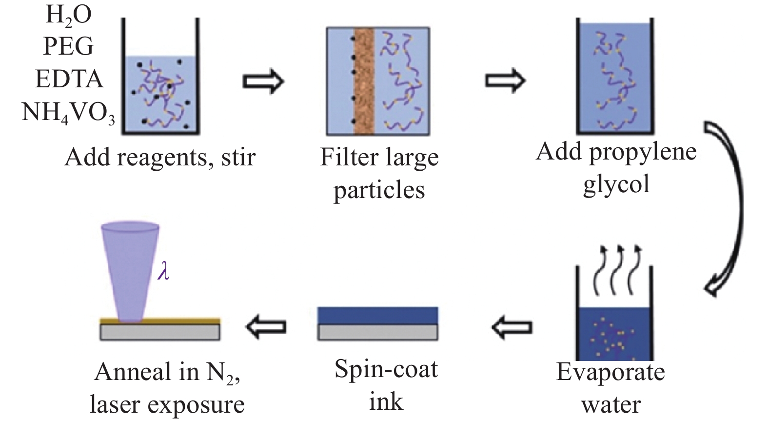
2017年,Breckenfeld等[29]研究证明有能力使用简单的市售试剂、相对较低的退火温度和非活性气体(N2)环境,通过聚合物辅助沉积工艺与激光加工相结合,可靠地合成多晶VO2薄膜,如图5所示。最佳条件下制备的薄膜,波长为2500 nm的激光相变前透光率为86%,相变后降至42%。该研究为在相对较低的温度下,潜在的大面积上快速、可靠地合成VO2薄膜的需求提供制备方法。
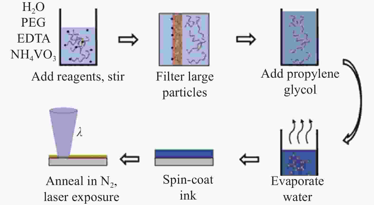
图 5 溶液混合和薄膜制备的过程
Figure 5. Process for solution mixing and film synthesis
2019年,Kim等[30]通过脉冲激光沉积技术在二氧化钛(TiO2)基底上沉积带有二氧化钌(RuO2)缓冲层的VO2薄膜。结果显示RuO2的厚度在50~10 nm之间变化时,VO2/RuO2/TiO2结构的对应相变温度范围为59~24 ℃。证明可以通过调整缓冲层的厚度,控制VO2薄膜和RuO2缓冲层之间的外延应变,从而调整VO2薄膜的相变温度。
2020年,Koussi等[31]通过脉冲激光沉积和快速热退火探讨VO2薄膜的制备。研究表明,低至350 ℃的快速热退火温度下,可以获得透射率变化40%左右的薄膜。通过选择基底和修改退火温度,可以控制相变温度和磁滞参数,能够获得低至52 ℃的相变温度和小至3 ℃的磁滞宽度。
2020年,Gurunatha等[32]通过控制热退火工艺中的真空度和退火温度来调节VO2材料的相变特性,结果显示温度引起的应力促进相变温度使其上升至79.5 ℃,而氧空位抑制相变温度使其降低至34.1 ℃,该工作为VO2的选择性相变以及控制相变温度提供可行的途径。
后续研究极有可能围绕VO2材料的可控加工制备展开,通过优化的加工制备参数操控VO2材料的相变温度和响应时间等性质,使得VO2材料更加适用于激光致盲防护。
-
VO2材料的相变特性被发现以来,其在激光致盲防护方面的应用研究从未间断,实验数据充分验证其激光致盲防护能力。
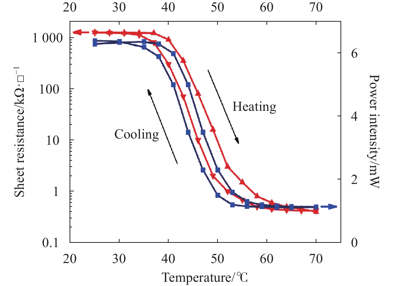
1996年,Choi等[33]利用脉冲激光沉积法在蓝宝石基底制备VO2薄膜,并测量60~90 ℃之间VO2薄膜的中红外波段透射率和反射光谱,结果显示随着温度增加,反射率上升而透过率下降,如图6所示。

图 6 加热过程中VO2薄膜在不同温度下中红外波段的反射率和透过率光谱
Figure 6. (a) Reflectance and (b) transmittance spectra of the VO2 film at selected temperatures during the heating process
2004年,Chen等[34]利用反应离子束溅射法在硅基底上制备VO2薄膜,薄膜的厚度约为100 nm。实验测定波长10.6 μm时,相变阈值约为0.85 W/cm2,半导体相VO2的透射率约为54%,金属相的透射率低至3%,证明VO2薄膜保护敏感的红外探测器免受激光致盲的能力。
2007年,陈学荣等[35]利用离子束溅射和退火工艺于K9玻璃基底上制备出氧化钒薄膜,其组成成分为VO2和V2O5,应用波长532 nm、脉宽10 ns的Nd:YAG倍频激光器测得其损伤阈值为21.9 mJ/cm2。
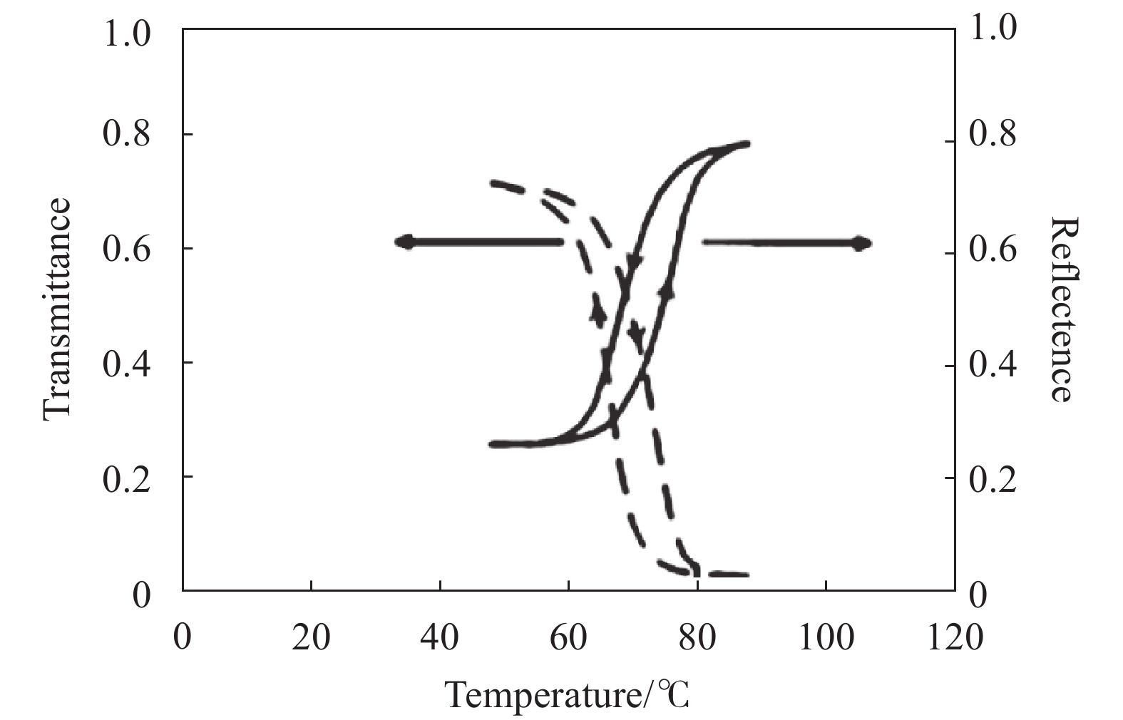
2012年,Huang等[36]通过直流磁控溅射技术和后退火工艺,制备出相变温度为45 ℃的VO2薄膜,并进行红外透射性能实验,实验光源采用波长3.39 μm、最大功率10 mW的氦氖激光器,结果如图7所示,相变前透过率达到63%,相变后透过率为11%,充分说明VO2薄膜是激光防护的潜力材料。

图 7 VO2薄膜的电学和光学性质
Figure 7. Electrical and optical properties of VO2 thin film
2016年,Vilanova等[37]通过测量增加激光功率时微拉曼光谱来研究强可见光对空气中VO2晶体的影响。激光波长632.8 nm、功率密度超过500 MW/m2时,激光加热诱导相变。激光功率密度超过1300 MW/m2时,激光加热会引起VO2与空气中的氧气的反应,并氧化成V2O5。
同年,王雅琴等[38]采用反应离子束溅射和后退火处理技术在石英玻璃基底上制备VO2薄膜。实验测得该薄膜3 μm波长处相变前透过率达到77%,相变后透过率为18%,且1.08 μm波长处相变阈值为4.35 W/cm2,损伤阈值为404 W/cm2。
2018年,侯典心等[39]利用直流磁控溅射法制备VO2薄膜,并使用泵浦探测技术研究1364 nm波长激光的能量密度对相变特性的影响。实验分析表明:激光能量大于30 mJ/cm2时,单次脉冲即可激发相变,相变响应时间约为14 ns,相变恢复时间与激光能量密度呈现自然指数关系,同时指出可以通过优化VO2基底材料参数来提高薄膜的激光防护能力。
同年,刘志伟等[40]利用分子束外延法制备Al2O3基底VO2薄膜,室温下对中红外波段的透过率达到>80%,其相变温度约为45 ℃,采用波长3459 nm、脉宽50 ns、重频50 kHz、功率密度0.14 W/cm2 的中红外激光实测得到薄膜调制深度达到>60%。同时发现薄膜越厚,相变前对中红外透过率越低,温滞宽度越宽,调制深度相对较低。仿真研究激光功率密度、薄膜基底厚度和薄膜初始温度等因素对相变时间的影响[41]。结果表明:增大功率密度、初始温度或者减小基底厚度可以缩短薄膜的相变时间,并且相变时间和功率密度是类似“指数衰减”关系。实验对比30 nm厚度VO2薄膜近红外和中红外波段透过率调制深度,结果表明:1 064 nm激光的最大透过率调制深度约为13%,而3459 nm激光的透过率调制深度约为62%,因此,VO2薄膜的1064 nm激光防护效果不理想[42]。
复合结构能够利用其他材料来改善和拓展VO2材料的激光致盲防护性能,因此,设计和制备复合结构是利用VO2材料进行光电成像系统激光致盲防护的重要发展方向。
2014年,Zhao等[43]致力于寻找一种可重复的、经济的溶液加工策略来制备VO2-SiO2复合薄膜,利用等效介质理论设计并实际制备出VO2-SiO2复合薄膜,Si/V摩尔比为0.8时,有效地将VO2薄膜可见光波段29.6%的平均透过率提高到48.5%,同时保留VO2薄膜相变前后红外波段透过率的变化特性,结果如图8所示。
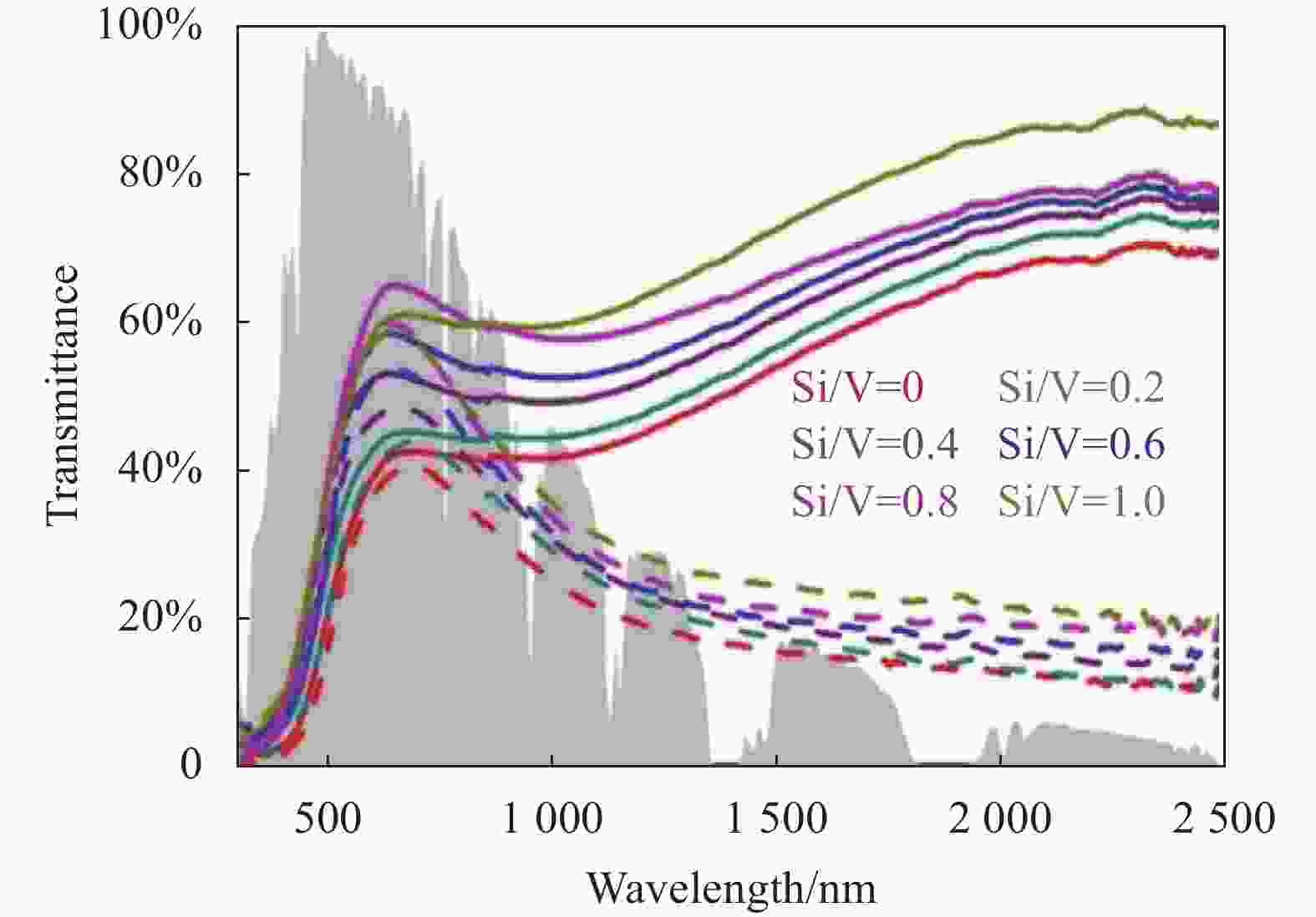
图 8 250~2 500 nm波长范围内增加Si/V摩尔比时VO2-SiO2复合膜的透射光谱。实线:30 ℃,虚线:100 ℃
Figure 8. Transmittance spectra of VO2-SiO2 composite films upon increasing Si/V molar ratios in the wavelength ranges from 250 nm to 2500 nm. Solid line: 30 ℃; Dash line: 100 ℃
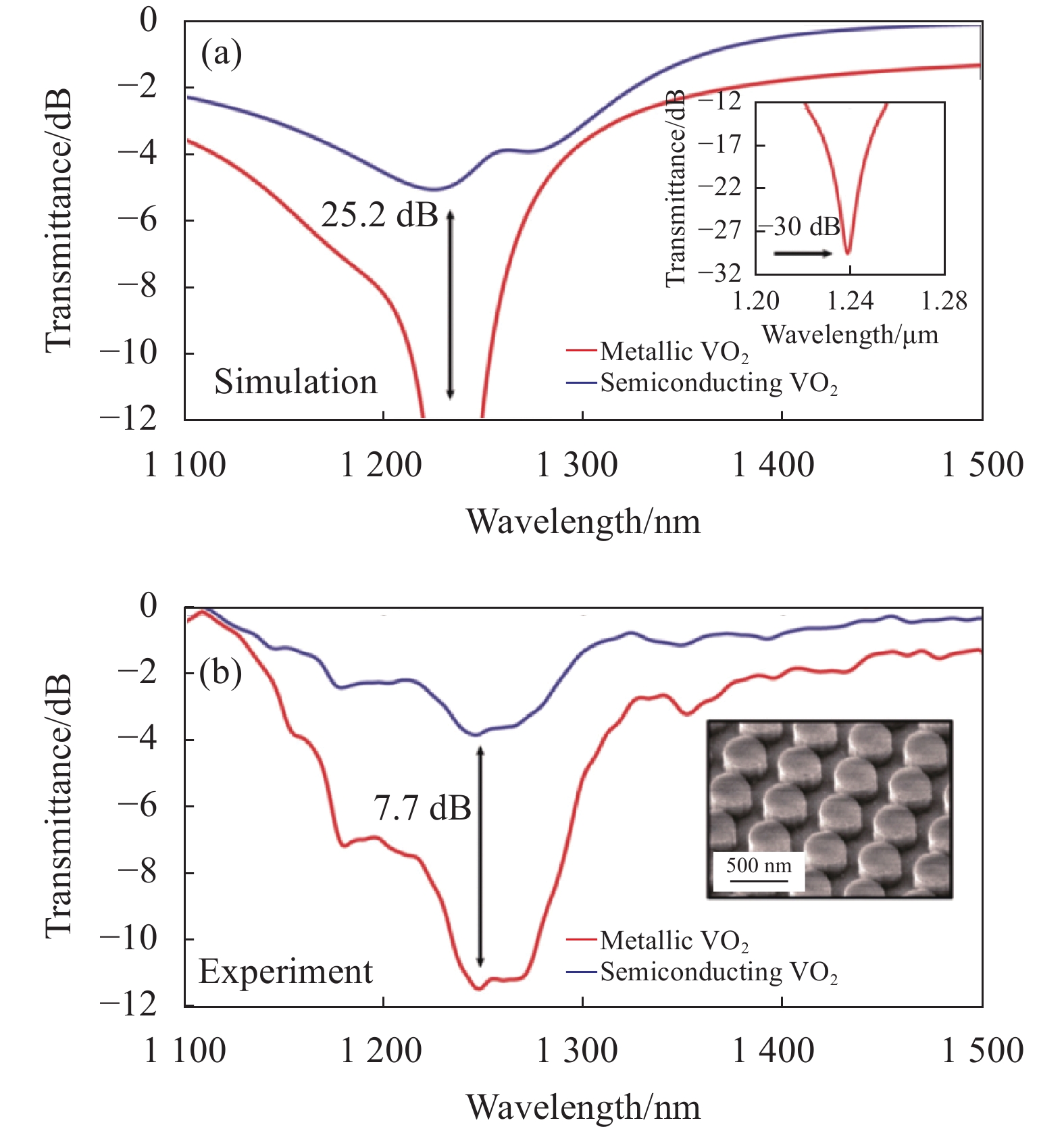
2020年,Howes等[44]提出一种VO2超表面光限幅器,仿真结果表明,工作波长为1.24 μm时,该光限幅器具有较高的开放态透过率(−4.8 dB)和较大的衰减比率(25.2 dB),实测样品得到开放态透过率与仿真结果一致,限制态透过率为−11.7 dB,计算得到衰减比率为7.7 dB,结果如图9所示。
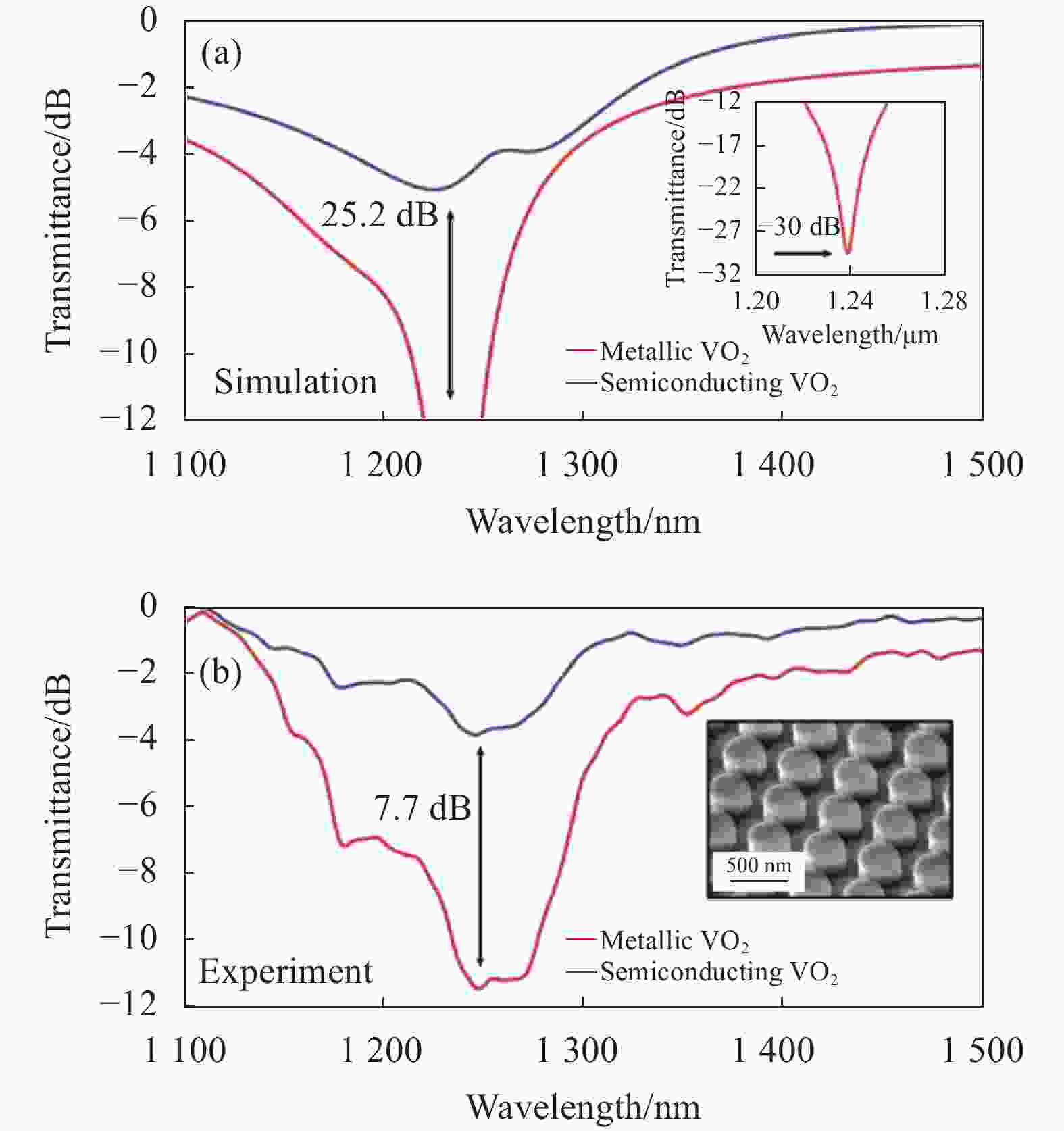
图 9 (a)仿真和(b)实验的限幅器开启和关闭状态时的透射率。(b)中插图为制造器件的SEM图像
Figure 9. (a) Simulated and (b) experimental transmittance of the limiter in the on and off-states. The inset in (b) is an SEM image of the fabricated device
2021年,Wan等[45]仿真设计基于VO2的金属频率选择表面(FSS)反射光限幅器(FSS-VO2 OL),设计波长为10.6 μm时,参数优化后能够达到≈0.7的开放态透射率、<0.01的限制态透射率、≈0.06的限制态吸收率和FWHM>2 μm的工作带宽。实验测量得到样品10.6 μm波长处的透过率为0.36,样品的峰值透过率偏移到9.8 μm处为0.45,分析造成峰值功率低于仿真数值的原因为忽略衬底背面的影响,造成峰值功率偏移的原因为金属频率选择表面尺寸误差和VO2折射率误差。
纳米尺度图案的制作相对复杂。2023年,Guan等[46]设计并制作具有宽带高开放态透过率的VO2光限幅器,该设计提供>−0.9 dB的开放态透光率和>21.8 dB的衰减比率,并显示出宽带(FWHM >3 μm)工作波长。实验表明该VO2光限幅器具有优异的红外成像性能,且仿真结果表明激光强度90 kW/cm2时,其具有0.23 μs的快速响应时间。该设计和制作方法为VO2光限幅器的近、远红外成像和激光保护提供平台。
-
计算成像技术[47-48]是多学科前沿交叉的新型成像技术,集光学、数学和信息技术于一体,以信息传递为准则,注重全链路一体化全局优化设计,在成像链路中引入主被动信息编码,实现信道扩容,提高信息维度,提升成像信息获取及解译能力。目前,传统的计算成像技术侧重于在信息域通过调控信息维度来拓展成像能力,突破成像极限,而很少从能量域角度研究计算成像技术的激光致盲防护机理和方法。
光学成像的基本原理是光学物像共轭关系。传统的光学成像系统易受激光损伤或者干扰的根本原因在于物像共轭关系是“点对点”映射,造成到达探测器表面的光学增益高。通过对入射光场进行相位调控,在图像传感器上将原有的“点对点”映射关系变成“点对面”的映射关系。由于在光学成像系统中引入的相位调制函数是经过特殊设计的,具有逆函数,对阵列图像传感器上“弥散”的中间像用相位逆函数进行重构就可以恢复物空间的本来面目。此时,如果有强激光入射,也会被弥散在图像传感器上一个较大区域内,使到达探测器表面上的功率/能量密度大大降低,由此可破解光电成像系统易受到激光致盲的难题。
-
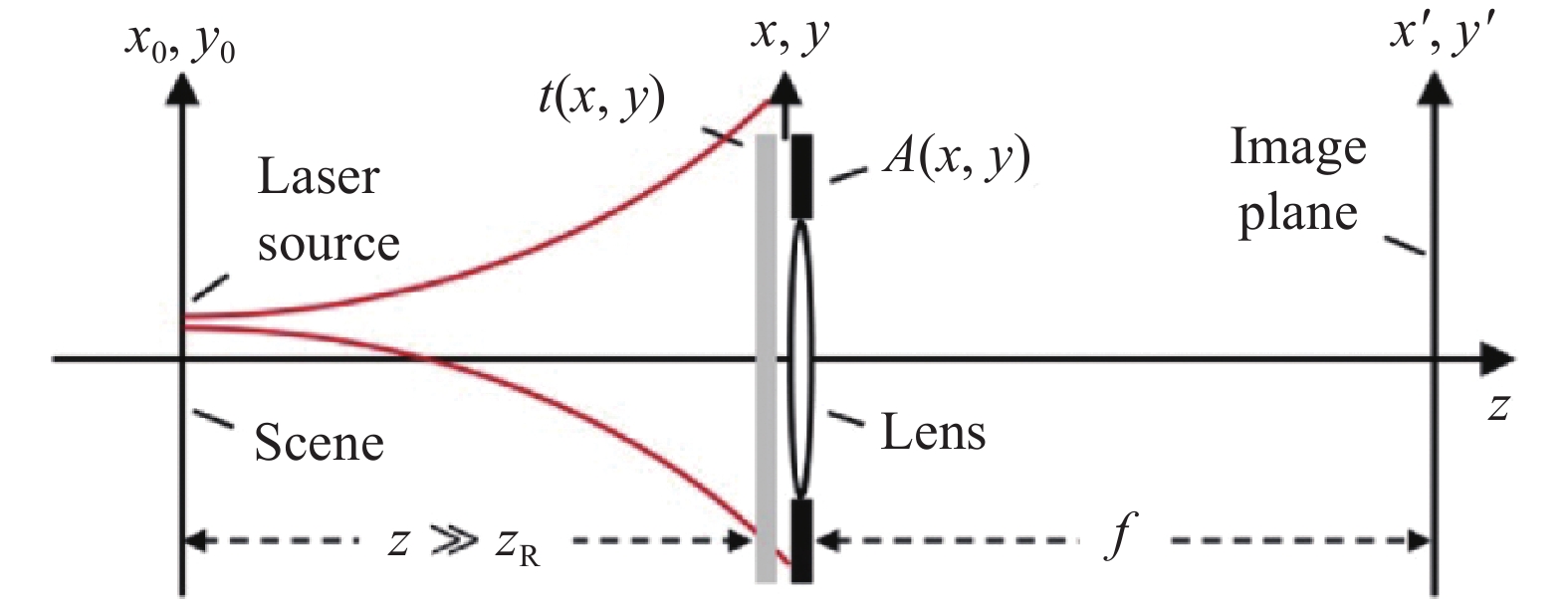
2015年,Ruane等[49]首次将计算成像技术引入激光防护领域,利用波前编码成像系统光瞳面上的涡旋和轴锥相位掩模调制致盲激光,光学系统结构如图10所示,致使探测器面上的光斑能量重新分布,实验测得拓扑荷$l = 18$的涡旋相位板可以有效降低峰值光强两个数量级,从而保护探测器免受损伤。
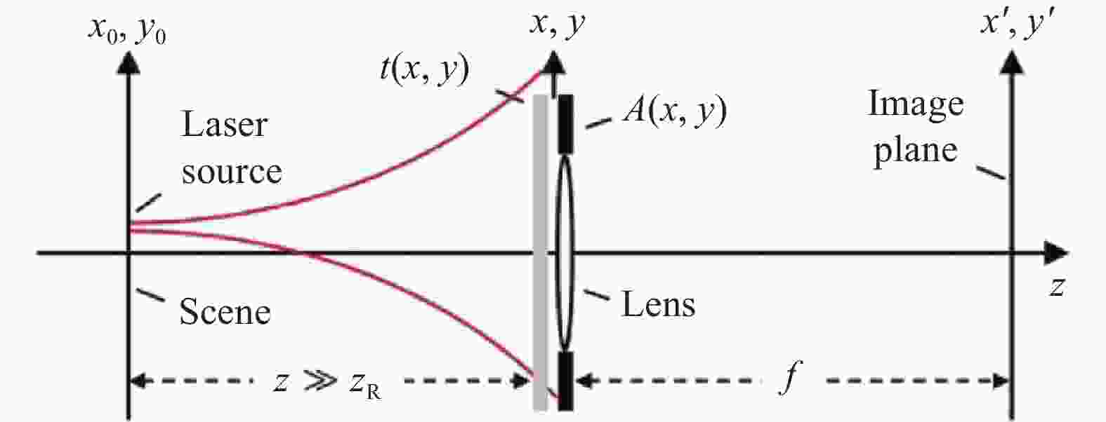
图 10 光学系统示意图
Figure 10. Diagram of the optical system
2016年,Watnik等[50]进一步研究该系统在激光辐照影响下的非相干成像情况,结果显示涡旋和轴锥相位掩模的波前编码成像系统都可以恢复非相干场景,同时比较涡旋和轴锥相位掩模的优缺点,轴锥相位掩模的低阶相位掩模的饱和度较低,高阶相位掩模的空间频率恢复较好,因此其性能优于涡旋相位掩模。
2017年,Wirth等[51]利用空间光调制器实验验证涡旋、轴锥和立方相位掩模的激光防护效果和成像效果。峰值光强降低约50倍的情况下,立方相位掩模经过维纳反卷积处理后的图像质量更好,可通过联合去卷积的操作改善涡旋和轴锥相位掩模的图像质量。
2018年,Wirth等[52]设计新的低峰值强度的点扩散函数,实验测试结果显示峰值强度降低100倍,且成功记录图像,充分说明波前编码成像系统的激光防护潜力。
2018年,Wang所在的课题组[53]设计并优化一种全新的反正弦型相位掩模板,在保证重构图像保真度和信噪比的前提下比三次相位板有更优越的焦深延拓性能,为采用计算成像方法开展激光致盲防护技术奠定理论基础。
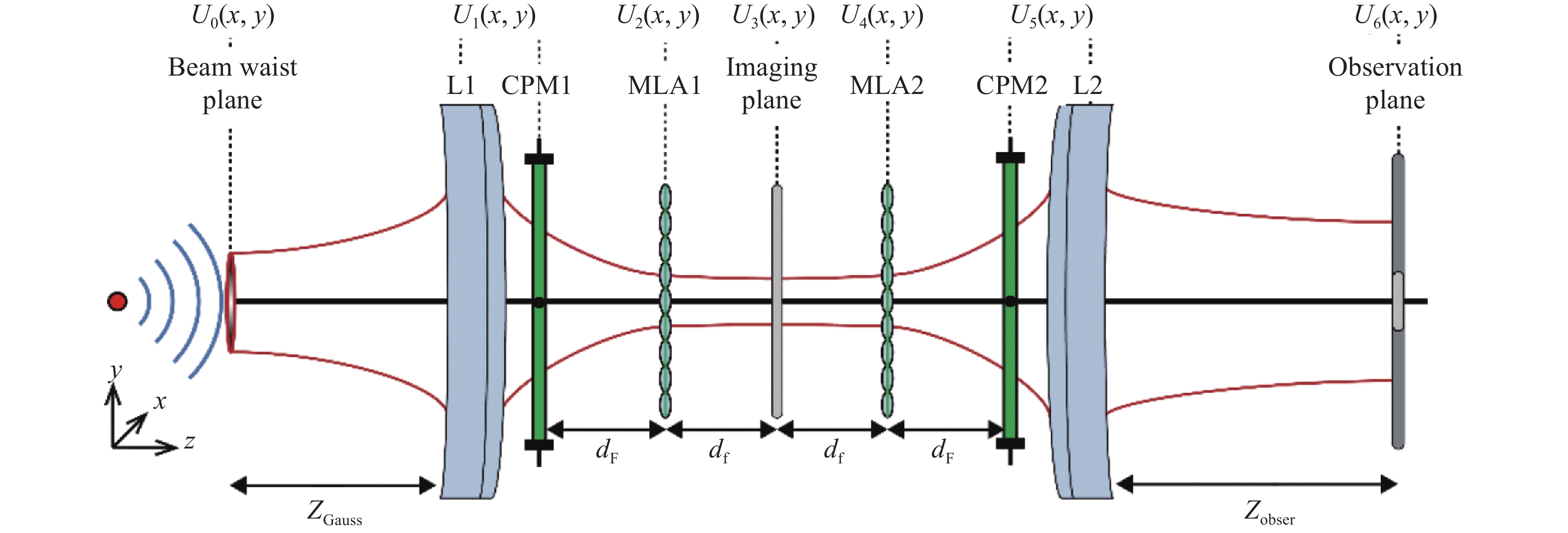
2019年,Wang所在的课题组[54]提出基于光场成像的激光致盲防护技术,可以将成像平面的最大单像素接收功率降低78%以上,进而可有效提高激光致盲阈值近一个数量级。紧接着,Wang所在的课题组[55]提出波前编码与光场复合成像系统,系统结构如图11所示,同样实现提升激光致盲阈值近一个数量级的效果。

图 11 复合成像系统的等效示意图
Figure 11. Equivalent schematic of the composite imaging system
2023年,Li所在的课题组[56]仿真对比六种相位掩模板的激光致盲防护性能,结果显示立方相位掩模板的激光致盲防护性能最好,成像平面最大单像素接收功率降幅约为95.00%。
基于防护材料的激光致盲防护技术不改变原有成像系统的物像关系,即不改变到达探测器表面的光强分布,只改变了到达探测表面的光强大小,因此对其防护性能评价往往关注材料对激光的限幅能力,评价指标采用调制深度等指标。而基于计算成像的激光致盲防护改变了原有成像系统的物像关系,到达探测器表面的光强分布与传统成像系统不同,因此,Ye所在的课题组[57]提出采用峰值光强或者最大单像素接收功率相对于传统成像系统的衰减倍率来衡量防护性能,并实验测量了采用立方相位掩模板后对CCD和CMOS探测器的防护能力提升程度。
综上所述,基于计算成像的激光致盲防护技术能够应用于可见光和红外等波段的防护,根据防护的目标成像系统的工作波段,可以灵活选择相位掩模板的制作材料。该技术能将峰值光强降低两个数量级,计算得到光学密度OD=2,而且其原理决定其能够实现瞬时响应。
横向比较基于相变材料的激光防致盲技术,VO2材料具有相变前后红外波段透过率突变的特性,因此可以应用于红外激光的防护,估算得到VO2材料的光学密度OD<1。VO2材料光致相变响应时间约为飞秒量级,热致相变响应时间约为毫秒量级。
此外,基于计算成像的激光致盲防护技术的防护性能取决于相位掩模板的相位函数,相位函数的巨大发展空间使得其更具发展潜力。
-
光电成像系统采用防护材料进行激光致盲防护时,材料对入射激光功率/能量密度的衰减倍率可能不够,使得到达探测器表面的能量密度低于致盲阈值而高于致眩阈值,此时激光致眩防护至关重要。光电成像系统采用计算成像方法进行激光致盲防护时,弥散的中间像保护探测器不被致盲的同时会增大探测器上叠加的激光光斑尺寸,造成致眩效应更加明显,因此必须开展激光致眩防护技术研究,去除饱和光斑对图像信息解译的影响。
光电成像系统致眩防护技术根据采用手段不同分为两类,一类是在图像端进行处理,另一类是通过前端光学系统设计并结合后端图像处理进行防护。图像处理激光致眩防护通常要求干扰光斑没有完全遮蔽目标信息,首先确定干扰光斑面积和光斑位置,然后采用例如数字日冕等技术对干扰光斑内图像进行恢复。光学系统设计激光致眩防护对干扰光斑大小和位置没有要求,适用范围更广,但是需要改变成像光路,系统复杂程度增加,其核心思想是利用成像光场与激光光场相干性的差异,通过对入射光场的频率调控,获得时空分离的光波谱段图像,并利用分离的谱段图像数据进行相关融合实现激光致眩干扰抑制和图像信息恢复,由此破解从激光(相干光)干扰中恢复出可见光(非相干光)目标图像信息的难题。
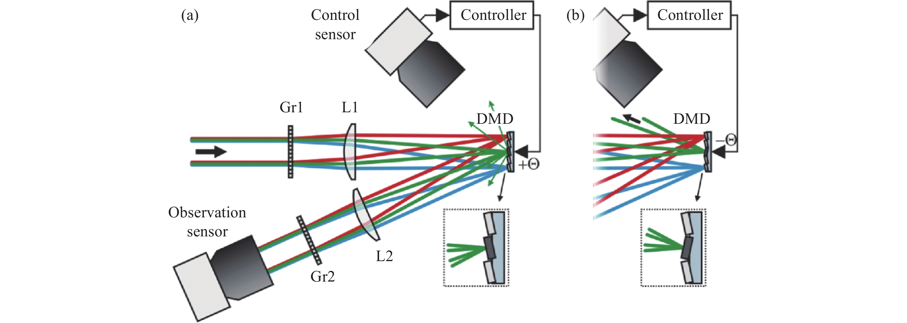
2011~2012年,Ritt等[58-59]提出结合波长复用与空间光调制器和结合波长复用与数字微镜装置的两种激光致眩防护方法,原理如图12所示,通过识别致眩激光波长,并控制位于光学系统中间焦平面位置的空间光调制器或数字微镜装置的对应单元进行选择性光谱滤波,阻断或反射致眩激光实现防护。该技术能够抑制视场内的致眩激光,且不丢失致眩激光区域的场景细节。但是该技术的响应时间约为几毫秒,意味着无法防护该时间内进入成像系统的脉冲激光。
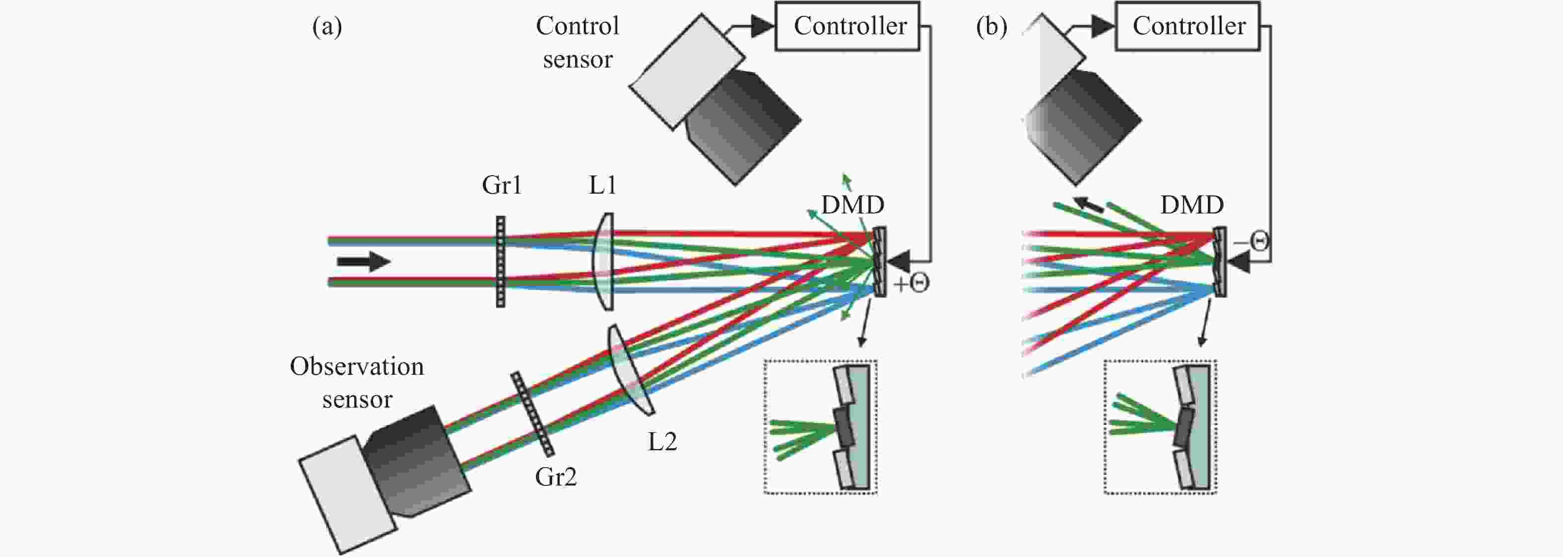
图 12 结合波长复用与数字微镜装置的激光致眩防护方法
Figure 12. Laser dazzling protection method combining digital micromirror device with the wavelength multiplexing technique
2017年,Schwarz等[60]研究上述激光致眩防护方法中的数字微镜装置的损伤阈值,结果表明:连续激光辐照0.25 s时,数字微镜装置的损伤阈值为(21.9±1.2) kW/cm2,大于彩色CCD的(14±2) kW/cm2的损伤阈值,但是小于黑白CCD、黑白CMOS和彩色CMOS的损伤阈值,其损伤阈值分别为(146±9) kW/cm2、(75±7) kW/cm2和(56.7±1.8) kW/cm2。
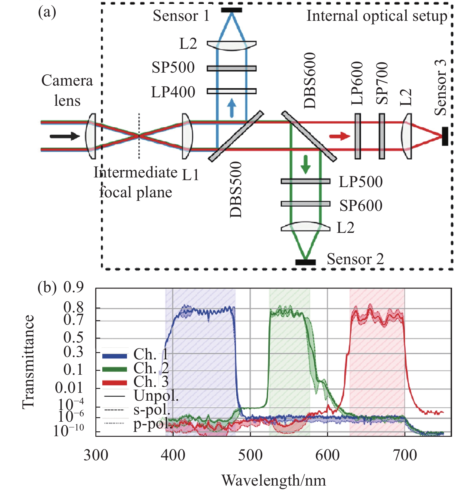
2019年,Ritt等[61]基于波段互补原理,提出在激光致眩情况下减少成像信息损失的三通道波段补偿成像方法,原理如图13所示。利用两个以上波段,波段的隔离度足够高,可以有效防止激光致眩成像传感器。同时,通过室内和室外实验证实该方法的有效性。
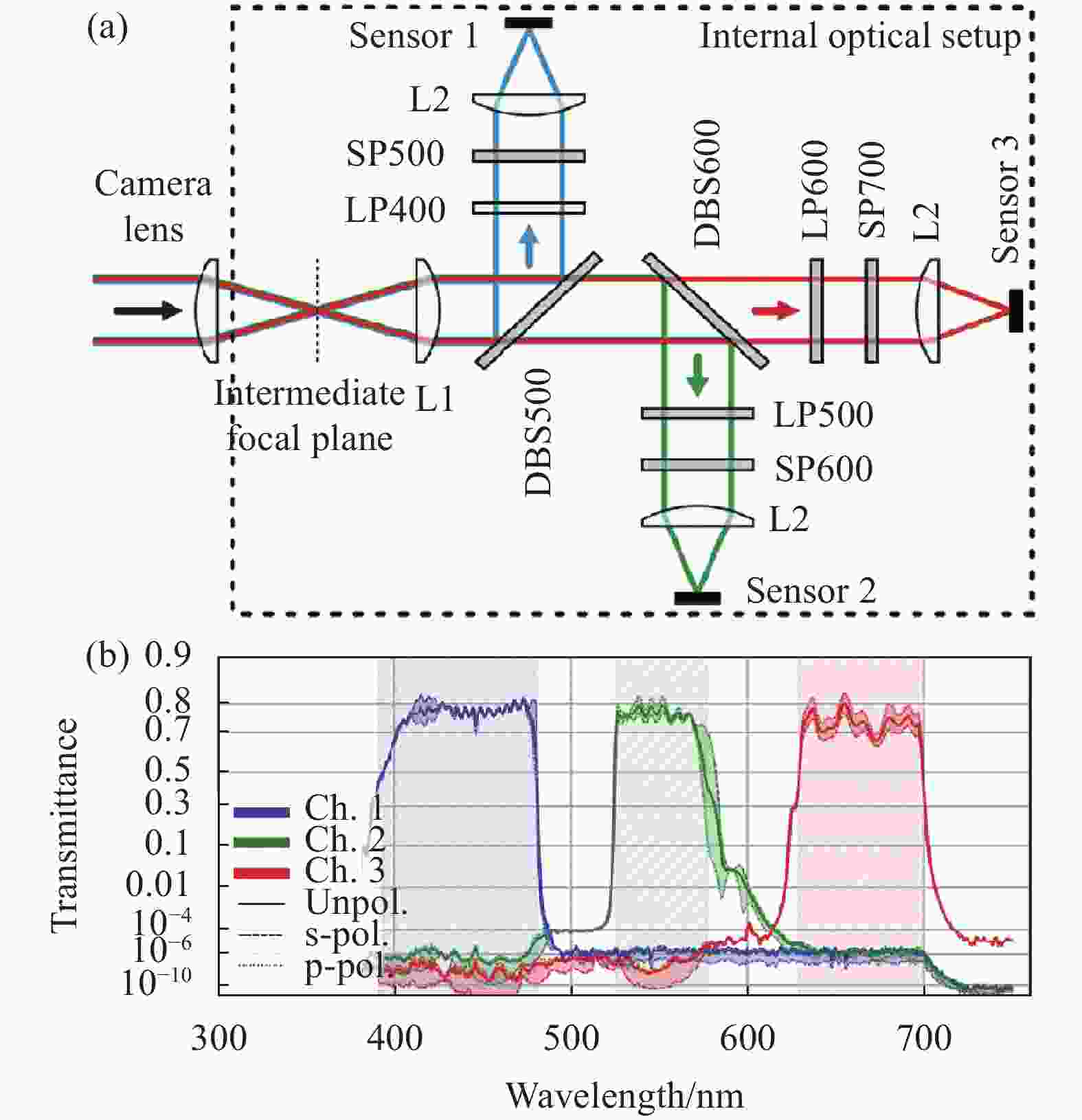
图 13 三通道波段补偿成像方法的光学布局示意图(a)及透过率函数(b)
Figure 13. (a) Optical layout diagram and (b) transmittance function of three-channel band compensation imaging method
2020年,Ritt等[62]系统提出三通道波段补偿成像方法和双通道波段补偿成像方法来减少激光致眩情况下成像信息的损失,其中三通道波段补偿成像方法三个分光路分别对三个波段进行成像,图像传感器采用单色相机,需要融合三个传感器的信息生成彩色图像,而双通道波段补偿成像方法两个分光路分别对多个波段进行成像,且波段互补,图像传感器采用彩色相机,图像传感器不需要进行信息融合便可成彩色像,双通道波段补偿成像方法的原理如图14所示。利用室内成像的结构相似度指标和室外场景成像的直观效果两个方面评价系统的激光致眩防护能力。
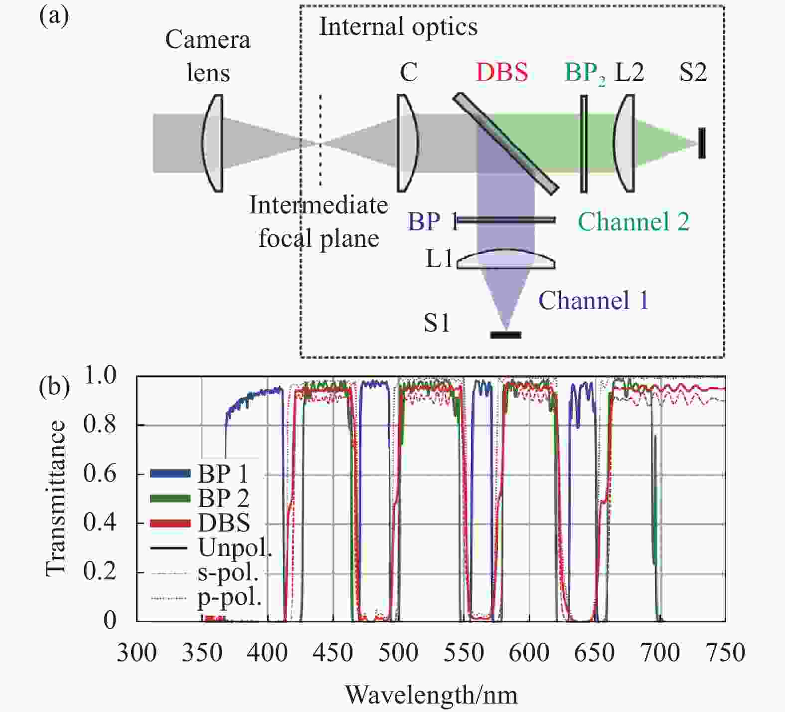
图 14 双通道波段补偿成像方法的光学布局示意图(a)及透过率函数(b)
Figure 14. (a) Optical layout diagram and (b) transmittance function of dual-channel band compensation imaging method
激光致眩防护技术的发展同时促进其性能评估方法逐渐趋于完善。2015年,Ritt等[63]提出两种激光致眩防护技术的性能评估方法,分别是三角形方向判别法和结构相似度法。2017年,Ritt等[64]进一步总结激光致眩防护的评价方法,包括饱和像元数法[65]、三角形方向判别法和结构相似度法[66]。并用这三种方法对结合波长复用与数字微镜装置的激光致眩防护方法,以及基于三通道波段补偿的激光致眩防护方法的实验研究数据进行评估,最后总结三种评价方式的优缺点。
-
综述了采用线性材料、非线性材料、相变材料、计算成像进行激光致盲防护的研究现状,介绍了激光致眩防护的可行技术。
基于线性材料的激光致盲防护技术优点是技术成熟,缺点只能对特定波长进行窄带滤光,形成对特定已知威胁激光的“有限谱段”的点防护,防护波长范围有限。基于非线性材料的激光致盲防护技术优点是防护谱段宽,在可见光-近红外谱段都可起到光限幅作用,但是非线性材料的固态化、实用化制备还在探索中。相变材料具有防护谱宽和光学密度大的优点,但是皮秒和飞秒量级脉宽激光技术的发展使得响应时间成为限制相变材料应用的关键因素,且相变材料无法同时具备高线性透过率、大动态范围和高损伤阈值等特性。通过控制加工条件操控VO2材料的防护技术指标以及设计和制备复合结构优化调整激光防护性能是重要的发展方向。
采用计算成像技术进行激光致盲防护是颠覆成像体制的技术方案,突出优点是防护谱段宽、适应性好,不需要像采用线性材料防护那样需要知道干扰激光位置、波长、偏振等先验信息,也不需要像采用非线性或相变材料防护那样需要考虑响应时间和防护阈值,既可防常见的连续激光和纳秒脉冲激光,也可以防正在蓬勃发展的皮秒或飞秒等超短脉冲激光。设计并高精度加工光场调控核心元件以及图像高质量恢复是该技术未来的重要发展方向。随着计算成像一个重要研究方向——掩模调制无透镜成像技术[67-68]的逐渐成熟,有望根本上解决成像系统中光学系统结构给光电传感器带来的高增益,从而彻底解决成像系统的激光致盲防护问题。
激光致眩防护技术应用场景比致盲防护技术更加广泛,但是目前研究相对较少,还未见颠覆性技术解决方案。根据激光对光电成像系统致盲和致眩机理来看,现在割裂研究光电成像系统致盲与致眩防护技术的方法是不完备,也是不科学的,未来需要进一步将光电成像系统激光致盲与致眩防护结合考虑,从防护机理、技术手段以及应用效费比等多层面深入研究。
Research progress of laser protection technology for optoelectronic imaging system (invited)
-
摘要: 随着激光技术的迅速发展,激光武器装备日益增多,广泛应用各个领域的光电成像系统被激光致盲或致眩的概率骤增,信息获取能力急剧下降,因此,光电成像系统激光防护技术研究变得越来越重要。简要介绍了基于线性材料和非线性材料的光电成像系统激光致盲防护技术的机理及局限,重点阐述了以二氧化钒为代表的基于相变材料的激光致盲防护技术的机理、制备方法和应用进展,详细分析了基于计算成像的激光致盲防护技术的机理和初步应用探索,结合激光致盲与致眩的关系补充说明了研究光电成像系统激光致眩防护技术的必要性和可行性,最后总结了光电成像系统各种激光防护技术的优缺点以及未来发展方向。Abstract:
Significance Optoelectronic imaging systems, characterized by their compact size, light weight, high reliability, resolution, and dynamic range, have been extensively employed in various fields, such as medical imaging, media production, security management, high-resolution target reconnaissance, precision guidance, fire control and targeting, and flight assistance. However, with the rapid advancements in laser technology and the widespread use of laser weapon systems, the risk of optoelectronic imaging systems being blinded or dazzled by lasers has significantly increased, resulting in a substantial decrease in information acquisition capabilities. Consequently, investigating laser protection technologies for optoelectronic imaging systems has become increasingly vital. Progress The article initially provides a brief overview of the mechanisms and limitations of laser blinding protection technologies for optoelectronic imaging systems, focusing on linear and nonlinear materials. It then delves into laser blinding protection technologies employing phase-change materials, such as vanadium dioxide, discusses their mechanisms, fabrication methods, and application progress. Subsequently, the article explores the mechanisms and preliminary application studies of laser blinding protection technologies based on computational imaging, highlights the necessity and feasibility of researching laser dazzling protection technologies for optoelectronic imaging systems in relation to laser blinding. Finally, the advantages and disadvantages of various laser protection technologies for optoelectronic imaging systems are summarized, along with potential future development directions. Conclusions and Prospects The application of computational imaging technology for laser protection offers a groundbreaking technical solution, featuring a wide protective spectrum and exceptional adaptability. This approach eliminates the need for prior knowledge of interfering laser locations, wavelengths, or polarization states, as required by linear material protection, as well as considerations of response times and protection thresholds, as demanded by nonlinear or phase-change material protection. Computational imaging technology can defend against common continuous lasers, nanosecond pulse lasers, and emerging ultra-short pulse lasers, such as picosecond or femtosecond pulses. Designing and fabricating high-precision optical field control components and ensuring high-quality image restoration are crucial future development directions for this technology. As lensless imaging technology employing mask modulation, a key research area in computational imaging progressively matures, it may fundamentally resolve the high gain caused by the optical system structure in imaging systems, thereby effectively addressing the issue of laser blinding protection in such systems. Laser dazzling protection technology exhibits broader application scenarios compared to blinding protection technology; However, current research is relatively limited, and no groundbreaking solutions have been proposed. Based on the mechanisms of laser-induced blinding and dazzling in optoelectronic imaging systems, the seperate study on blinding and dazzling technologies is incomplete and unscientific. Future research should focus on integrating laser blinding and dazzling protection for optoelectronic imaging systems, examining protection mechanisms, technical approaches, and cost-effectiveness from multiple perspectives. -
Key words:
- optoelectronic imaging system /
- laser blinding /
- laser dazzling /
- laser protection
-
图 2 (a)泵浦脉冲的高斯空间轮廓; (b)相变过程中的反射率变化; (c)样品上三个不同位置的反射率的时间分辨演变,对应的能量密度为(c1) 7 mJ/cm2、(c2) 15 mJ/cm2和(c3) 25 mJ/cm2
Figure 2. (a) Gaussian spatial profile of pumping pulse; (b) Reflectivity during the phase transformation; (c) Time resolved evolutions of the reflectivity for three different positions on the sample, corresponding to local fluences of (c1) 7 mJ/cm2, (c2) 15 mJ/cm2, and (c3) 25 mJ/cm2
图 3 光致相变的响应时间与脉宽的函数关系,脉宽位于1.5 ps~15 fs之间
Figure 3. Response time of photoinduced transition as a function of pulse width, which ranges from 1.5 ps to 15 fs
图 6 加热过程中VO2薄膜在不同温度下中红外波段的反射率和透过率光谱
Figure 6. (a) Reflectance and (b) transmittance spectra of the VO2 film at selected temperatures during the heating process
图 8 250~2 500 nm波长范围内增加Si/V摩尔比时VO2-SiO2复合膜的透射光谱。实线:30 ℃,虚线:100 ℃
Figure 8. Transmittance spectra of VO2-SiO2 composite films upon increasing Si/V molar ratios in the wavelength ranges from 250 nm to 2500 nm. Solid line: 30 ℃; Dash line: 100 ℃
图 9 (a)仿真和(b)实验的限幅器开启和关闭状态时的透射率。(b)中插图为制造器件的SEM图像
Figure 9. (a) Simulated and (b) experimental transmittance of the limiter in the on and off-states. The inset in (b) is an SEM image of the fabricated device
图 12 结合波长复用与数字微镜装置的激光致眩防护方法
Figure 12. Laser dazzling protection method combining digital micromirror device with the wavelength multiplexing technique
图 13 三通道波段补偿成像方法的光学布局示意图(a)及透过率函数(b)
Figure 13. (a) Optical layout diagram and (b) transmittance function of three-channel band compensation imaging method
图 14 双通道波段补偿成像方法的光学布局示意图(a)及透过率函数(b)
Figure 14. (a) Optical layout diagram and (b) transmittance function of dual-channel band compensation imaging method
表 1 光致相变的响应时间相关研究
Table 1. Studies on response time of photoinduced transition
Sample property Synthesis method Test condition Response time Reference 32 nm-thick
VO2 thin filmLow-temperature process Pulse width: 450-550 fs
Energy density: 3.7 mJ/cm2
Wavelength: 780 nm<500 fs [16] 0.2 μm-thick
VO2 thin filmReaction evaporation deposition and annealing Biasing temperature: 52 ℃
Pulse width: 50 ns
Energy density: 150 mJ/cm2<50 ns [17] 0.2 μm-thick
VO2 thin film- Pulse width: 50 fs
Energy density: 7-25 mJ/cm2
Wavelength: 800 nm50 ps-100 fs [18] VO2-Si3N4 structures Chemically etching Pulse width: 100 fs
Energy density: 50 mJ/cm2
Wavelength: 790 nm<500 fs [19] VO2 microcrystals Vapour transport Pulse width: ~45 fs
Energy density: 3.3 mJ/cm2
Wavelength: 800 nmFemtosecond timescale [20] 25 nm-thick
VO2 thin filmPulsed laser deposition Pulse width: 4.9 fs
Pulse energy: ~100 mJ/cm2
Wavelength: 400-1000 nm(26±6) fs [21] 75 nm-thick
VO2 thin filmPulsed laser deposition and annealing Wavelength: 800 nm 200 fs [22]  下载: 导出CSV
-
[1] Yu Q H, Xiao X S, Chen F S, et al. Co-design method for electro-optical imaging systems [J]. Journal of Infrared and Millimeter Waves, 2019, 38(6): 728-732. doi: 10.11972/j.issn.1001-9014.2019.06.008 [2] Svensson S, Bjorkert S, Kariis H, et al. Countering laser pointer threats to road safety[C]//Conference on Optics for Counter-terrorism and Crime Fighting II, 2006, 6402: 640207. [3] Jackson S D. Towards high-power mid-infrared emission from a fibre laser [J]. Nature Photonics, 2012, 6(7): 423-431. doi: 10.1038/nphoton.2012.149 [4] Hong L, Hu C, Liu Y, et al. 350-2500 nm supercontinuum white laser enabled by synergic high-harmonic generation and self-phase modulation [J]. PhotoniX, 2023, 4(1): 11. doi: 10.1186/s43074-023-00088-2 [5] 吕跃广, 孙晓泉. 激光对抗原理与应用[M]. 北京: 国防工业出版社, 2015. [6] 姜玉刚, 刘华松, 王利栓, 等. 卫星激光防护薄膜窗口的设计与制备技术研究[J]. 中国光学, 2019, 12(04): 804-809. doi: 10.3788/co.20191204.0804 Jiang Yugang, Liu Huasong, Wang Lishuan, et al. Design and preparation technology of laser protective film window of satellite [J]. Chinese Optics, 2019, 12(4): 804-809. (in Chinese) doi: 10.3788/co.20191204.0804 [7] 孙希鹏, 李晓东, 杜永超. 空间三结太阳电池用激光防护盖片研究[J]. 电源技术, 2021, 45(09): 1160-1163. doi: 10.3969/j.issn.1002-087X.2021.09.017 Sun Xipeng, Li Xiaodong, Du Yongchao. Research of laser protection coverglass for space triple junction solar cells [J]. Chinese Journal of Power Sources, 2021, 45(9): 1160-1163. (in Chinese) doi: 10.3969/j.issn.1002-087X.2021.09.017 [8] 张岩松, 温万田. 激光防护材料的研究现状及发展趋势[J]. 光电技术应用, 2004(05): 40-43. doi: 10.3969/j.issn.1673-1255.2004.05.011 Zhang Yansong, Wen Wantian. Research and development of laser protective materials [J]. Electro-Optic Technology Application, 2004(5): 40-43. (in Chinese) doi: 10.3969/j.issn.1673-1255.2004.05.011 [9] 国耀宇, 赵亚丽, 梁秀兵, 等. 用于多波段激光防护的聚碳酸酯眼镜片材料研究[J]. 航天医学与医学工程, 2016, 29(05): 353-356. doi: 10.16289/j.cnki.1002-0837.2016.05.008 Guo Yaoyu, Zhao Yali, Liang Xiubing, et al. Study on polycarbonate-based spectacle lens materials for multi-wavelength laser protection [J]. Space Medicine & Medical Engineering, 2016, 29(5): 353-356. (in Chinese) doi: 10.16289/j.cnki.1002-0837.2016.05.008 [10] 郑佳艺, 马壮, 高丽红. 智能化高能激光防护材料新进展[J]. 现代技术陶瓷, 2020, 41(03): 121-133. doi: 10.16253/j.cnki.37-1226/tq.2020.03.001 Zheng Jiayi, Ma Zhuang, Gao Lihong. Development of intelligent anti-high power laser materials [J]. Advanced Ceramics, 2020, 41(3): 121-133. (in Chinese) doi: 10.16253/j.cnki.37-1226/tq.2020.03.001 [11] 吕泽, 方佑, 冯迢, 等. 非线性光限幅材料原理、性能表征及研究进展[J]. 中国光学, 2022, 15(04): 625-639. doi: 10.37188/CO.2021-0195 Lv Ze, Fang You, Feng Tiao, et al. The principle, performance characterization and research progress of nonlinear optical limiting materials [J]. Chinese Optics, 2022, 15(4): 625-639. (in Chinese) doi: 10.37188/CO.2021-0195 [12] 董宁宁, 刘强虎, 王俊. 二维非线性光限幅材料研究进展[J]. 中国激光, 2021, 48(13): 7-21. doi: 10.3788/CJL202148.1300001 Dong Ningning, Liu Qianghu, Wang Jun. Research progress of two-dimensional nonlinear optical limiting material [J]. Chinese Journal of Lasers, 2021, 48(13): 1300001. (in Chinese) doi: 10.3788/CJL202148.1300001 [13] 张盛. V2O5/金刚石膜系多波段激光致盲防护基础研究[D]. 南京航空航天大学, 2019. Zhang Sheng. Basic research on V2O5/diamond films inmultiband laser blinding protection[D]. Nanjing: Nanjing University of Aeronautics and Astronautics, 2019. (in Chinese) [14] Morin F J. Oxides which show a metal-to-insulator transition at the neel temperature [J]. Physical Review Letters, 1959, 3(1): 34-36. doi: 10.1103/PhysRevLett.3.34 [15] Baum P, Yang D S, Zewail A H. 4D visualization of transitional structures in phase transformations by electron diffraction [J]. Science, 2007, 318(5851): 788-792. doi: 10.1126/science.1147724 [16] Becker M F, Bruce A B, Walser R M. Femtosecond laser excitation of the semiconductor-metal phase transition in VO2 [J]. Applied Physics Letters, 1994, 65(12): 1507-1507. doi: 10.1063/1.112974 [17] 查子忠, 王骐, 李学春, 等. VO2薄膜对TEACO2激光响应特性的实验研究[J]. 光学学报, 1996(08): 151-154. doi: 10.3321/j.issn:0253-2239.1996.08.030 Zha Zizong, Wang Qi, Li Xuechun, et al. Experemental study of response properties of VO2 films to TEA CO2 laser [J]. Acta Optica Sinica, 1996, 16(8): 151-154. (in Chinese) doi: 10.3321/j.issn:0253-2239.1996.08.030 [18] Cavalleri A, Toth C, Siders C W, et al. Femtosecond structural dynamics in VO2 during an ultrafast solid-solid phase transition [J]. Physical Review Letters, 2001, 87(23): 237401. doi: 10.1103/PhysRevLett.87.237401 [19] Cavalleri A, Dekorsy T, Chong H H W, et al. Evidence for a structurally-driven insulator-to-metal transition in VO2: A view from the ultrafast timescale [J]. Physical Review B, 2004, 70(16): 161102. doi: 10.1103/PhysRevB.70.161102 [20] O'callahan B T, Jones A C, Park J H, et al. Inhomogeneity of the ultrafast insulator-to-metal transition dynamics of VO2 [J]. Nature Communications, 2015, 6: 6849. doi: 10.1038/ncomms7849 [21] Jager M F, Ott C, Kraus P M, et al. Tracking the insulator-to-metal phase transition in VO2 with few-femtosecond extreme UV transient absorption spectroscopy [J]. Proceedings of the National Academy of Sciences of the United States of America, 2017, 114(36): 9558-9563. doi: 10.1073/pnas.1707602114 [22] Johnson A S, Perez-Salinas D, Siddiqui K M, et al. Ultrafast X-ray imaging of the light-induced phase transition in VO2 [J]. Nature Physics, 2023, 19: 215-220. doi: https://doi.org/10.1038/s41567-022-01848-w [23] Guiton B S, Gu Q, Prieto A L, et al. Single-crystalline vanadium dioxide nanowires with rectangular cross sections [J]. Journal of the American Chemical Society, 2005, 127(2): 498-499. doi: 10.1021/ja045976g [24] Rana R S, Nolte D D, Chudnovskii F A. Optical bistability from a thermodynamic phase transition in vanadium dioxide [J]. Optics Letters, 1992, 17(19): 1385-1387. doi: 10.1364/OL.17.001385 [25] Wang W, Luo Y, Zhang D, et al. Dynamic optical limiting experiments on vanadium dioxide and vanadium pentoxide thin films irradiated by a laser beam [J]. Applied Optics, 2006, 45(14): 3378-3381. doi: 10.1364/AO.45.003378 [26] Wang Z X, Ji X W, Dong N N, et al. Femtosecond laser-induced phase transition in VO2 films [J]. Optics Express, 2022, 30(26): 47421-47429. doi: 10.1364/OE.477910 [27] Nag J, Haglund R F. Synthesis of vanadium dioxide thin films and nanoparticles [J]. Journal of Physics-condensed Matter, 2008, 20(26): 264016. doi: 10.1088/0953-8984/20/26/264016 [28] 石倩倩, 王江, 程光华. 二氧化钒薄膜的制备技术及应用进展[J]. 光子学报, 2022, 51(10): 340-358. doi: 10.3788/gzxb20225110.1016002 Shi Qianqian, Wang Jiang, Cheng Guanghua. Preparation technology and application of vanadium dioxide thin films [J]. Acta Photonica Sinica, 2022, 51(10): 1016002. (in Chinese) doi: 10.3788/gzxb20225110.1016002 [29] Breckenfeld E, Kim H, Gorzkowski E P, et al. Laser-processing of VO2 thin films synthesized by polymer-assisted-deposition [J]. Applied Surface Science, 2017, 397: 152-158. doi: 10.1016/j.apsusc.2016.11.113 [30] Kim H, Charipar N A, Figueroa J, et al. Control of metal-insulator transition temperature in VO2 thin films grown on RuO2/TiO2 templates by strain modification [J]. AIP Advances, 2019, 9(1): 015302. doi: 10.1063/1.5083848 [31] Koussi E K, Bourquard F, Tite T, et al. Synthesis of vanadium oxides by pulsed laser deposition and rapid thermal annealing [J]. Applied Surface Science, 2020, 521: 146267. doi: 10.1016/j.apsusc.2020.146267 [32] Gurunatha K L, Sathasivam S, Li J W, et al. Combined effect of temperature induced strain and oxygen vacancy on metal-insulator transition of VO2 colloidal particles [J]. Advanced Functional Materials, 2020, 30(49): 2005311. doi: 10.1002/adfm.202005311 [33] Choi, Ahn, Jung, et al. Mid-infrared properties of a VO2 film near the metal-insulator transition [J]. Physical Review B, Condensed Matter, 1996, 54(7): 4621-4628. doi: 10.1103/PhysRevB.54.4621 [34] Chen S H, Ma H, Yi X J, et al. Smart VO2 thin film for protection of sensitive infrared detectors from strong laser radiation [J]. Sensors And Actuators A-physical, 2004, 115(1): 28-31. doi: 10.1016/j.sna.2004.03.018 [35] 陈学荣, 胡军志, 韩文政. 氧化钒薄膜脉冲激光损伤研究[J]. 材料热处理学报, 2007, 100(04): 122-124. doi: 10.3969/j.issn.1009-6264.2007.04.027 Chen Xuerong, Hu Junzhi, Han Wenzheng. Study on pulse laser damage of vanadium oxide thin film [J]. Transactions of Materials and Heat Treatment, 2007, 100(4): 122-124. (in Chinese) doi: 10.3969/j.issn.1009-6264.2007.04.027 [36] Huang Z L, Chen S H, Lv C H, et al. Infrared characteristics of VO2 thin films for smart window and laser protection applications [J]. Applied Physics Letters, 2012, 101(19): 191905. doi: 10.1063/1.4766287 [37] Vilanova-martinez P, Hernandez-velasco J, Landa-canovas A R, et al. Laser heating induced phase changes of VO2 crystals in air monitored by Raman spectroscopy [J]. Journal of Alloys and Compounds, 2016, 661: 122-125. doi: 10.1016/j.jallcom.2015.11.174 [38] 王雅琴, 姚刚, 黄子健, 等. 用于红外激光防护的高开关率VO2薄膜[J]. 物理学报, 2016, 65(05): 268-273. doi: 10.7498/aps.65.057102 Wang Yaqin, Yao Gang, Huang Zijian, et al. Infrared laser protection of multi-wavelength with high optical switching efficiency VO2 film [J]. Acta Physica Sinica, 2016, 65(5): 268-273. (in Chinese) doi: 10.7498/aps.65.057102 [39] 侯典心, 路远, 冯云松, 等. 采用泵浦探测技术研究VO2薄膜相变特性[J]. 发光学报, 2018, 39(02): 140-147. doi: 10.3788/fgxb20183902.0140 Hou Dianxin, Lu Yuan, Feng Yunsong, et al. Study on phase transition properties of VO2 based on pump-probe technique [J]. Chinese Journal of Luminescence, 2018, 39(2): 140-147. (in Chinese) doi: 10.3788/fgxb20183902.0140 [40] 刘志伟, 路远, 侯典心, 等. MBE法制备VO2薄膜及其中红外调制深度测量[J]. 发光学报, 2018, 39(07): 942-947. doi: 10.3788/fgxb20183907.0942 Liu Zhiwei, Lu Yuan, Hou Dianxin, et al. VO2 thin films prepared by MBE and measurements of mid-infrared modulation depth [J]. Chinese Journal of Luminescence, 2018, 39(7): 942-947. (in Chinese) doi: 10.3788/fgxb20183907.0942 [41] 刘志伟, 路远, 冯云松, 等. VO2薄膜受脉冲激光辐照实验及理论计算[J]. 光子学报, 2018, 47(10): 109-115. doi: 10.3788/gzxb20184710.1031001 Liu Zhiwei, Lu Yuan, Feng Yunsong, et al. Experiments and theoretical calculations of VO2 thin film irradiated by pulse laser [J]. Acta Photonica Sinica, 2018, 47(10): 1031001. (in Chinese) doi: 10.3788/gzxb20184710.1031001 [42] 刘志伟, 路远, 侯典心, 等. 激光辐照VO2薄膜温度场分布及透射特性研究[J]. 发光学报, 2018, 39(11): 1604-1612. doi: 10.3788/fgxb20183911.1604 Liu Zhiwei, Lu Yuan, Hou Dianxin, et al. Temperature field distribution and transmittance characteristics of VO2 films irradiated by laser [J]. Chinese Journal of Luminescence, 2018, 39(11): 1604-1612. (in Chinese) doi: 10.3788/fgxb20183911.1604 [43] Zhao L L, Miao L, Liu C Y, et al. Solution-processed VO2-SiO2 composite films with simultaneously enhanced luminous transmittance, solar modulation ability and anti-oxidation pro-perty [J]. Scientific Reports, 2014, 4(1): 7000. doi: 10.1038/srep07000 [44] Howes A, Zhu Z H, Curie D, et al. Optical limiting based on huygens' metasurfaces [J]. Nano Letters, 2020, 20(6): 4638-4644. doi: 10.1021/acs.nanolett.0c01574 [45] Wan C, Zhang Z, Salman J, et al. Ultrathin broadband reflective optical limiter [J]. Laser & Photonics Reviews, 2021, 15(6): 2100001. doi: https://doi.org/10.1002/lpor.202100001 [46] Guan H, Ren F, Liang S, et al. Ultra-high transmission broadband tunable VO2 optical limiter [J]. Laser & Photonics Reviews, 2023, 17(4): 2200653. doi: https://doi.org/10.1002/lpor.202200653 [47] 邵晓鹏, 刘飞, 李伟, 等. 计算成像技术及应用最新进展[J]. 激光与光电子学进展, 2020, 57(02): 11-55. doi: 10.3788/LOP57.020001 Shao Xiaopeng, Liu Fei, Li Wei, et al. Latest progress in computational imaging technology and application [J]. Laser & Optoelectronics Progress, 2020, 57(2): 020001. (in Chinese) doi: 10.3788/LOP57.020001 [48] 邵晓鹏, 苏云, 刘金鹏, 等. 计算成像内涵与体系[J]. 光子学报, 2021, 50(05): 9-31. doi: 10.3788/gzxb20215005.0511001 Shao Xiaopeng, Su Yun, Liu Jinpeng, et al. Connotation and system of computational imaging [J]. Acta Photonica Sinica, 2021, 50(5): 0511001. (in Chinese) doi: 10.3788/gzxb20215005.0511001 [49] Ruane G J, Watnik A T, Swartzlander G A. Reducing the risk of laser damage in a focal plane array using linear pupil-plane phase elements [J]. Applied Optics, 2015, 54(2): 210-218. doi: 10.1364/AO.54.000210 [50] Watnik A T, Ruane G J, Swartzlander G A. Incoherent imaging in the presence of unwanted laser radiation: vortex and axicon wavefront coding [J]. Optical Engineering, 2016, 55(12): 123102. doi: https://doi.org/10.1117/1.OE.55.12.123102 [51] Wirth J H, Watnik A T, Swartzlander G A. Experimental observations of a laser suppression imaging system using pupil-plane phase elements [J]. Applied Optics, 2017, 56(33): 9205-9211. doi: 10.1364/AO.56.009205 [52] Wirth J H, Watnik A T, Swartzlander G A. Computational imaging for reducing peak irradiance on focal planes[C]//Computational Imaging III, 2018, 10669: 106690U. [53] Wang L, Ye Q, Nie J S, et al. Optimized asymmetrical arcsine phase mask for extending the depth of field [J]. IEEE Photonics Technology Letters, 2018, 30(14): 1309-1312. doi: 10.1109/LPT.2018.2845709 [54] Wang L, Ye Q, Dou X, et al. Anti-cat-eye effect imaging technique based on the light-field imaging technique [J]. Journal of Electronic Imaging, 2019, 28(5): 053020. doi: https://doi.org/10.1117/1.JEI.28.5.053020 [55] Wang L, Dou X N, Ye Q, et al. Wavefront coded light-field imaging system to achieve substantial retroreflection reduction and anti-laser blinding property [J]. Optik, 2019, 192: 8. doi: https://doi.org/10.1016/j.ijleo.2019.162947 [56] Li Y, Ye Q, Wang L, et al. Analysis of laser-protection performance of asymmetric-phase-mask wavefront-coding imaging systems [J]. Current Optics and Photonics, 2023, 7(1): 1-14. [57] Ye Q, Wu Y, Zhang H, et al. Experimental damage thresholds of a laser suppression imaging system using cubic phase plate [J]. Chinese Optics Letters, 2023, 21(4): 041403. doi: 10.3788/COL202321.041403 [58] Ritt G, Eberle B. Electro-optical sensor with spatial and spectral filtering capability [J]. Applied Optics, 2011, 50(21): 3847-3853. doi: 10.1364/AO.50.003847 [59] Ritt G, Eberle B. Automatic suppression of intense mono-chromatic light in electro-optical sensors [J]. Sensors, 2012, 12(10): 14113-14128. doi: 10.3390/s121014113 [60] Schwarz B, Ritt G, Koerber M, et al. Laser-induced damage threshold of camera sensors and micro-optoelectromechanical systems [J]. Optical Engineering, 2017, 56(3): 034108. doi: https://doi.org/10.1117/1.OE.56.3.034108 [61] Ritt G, Schwarz B, Eberle B. Preventing image information loss of imaging sensors in case of laser dazzle [J]. Optical Engineering, 2019, 58(1): 013109. doi: https://doi.org/10.1117/1.OE.58.1.013109 [62] Ritt G, Eberle B. Use of complementary wavelength bands for laser dazzle protection [J]. Optical Engineering, 2020, 59(1): 015106. doi: https://doi.org/10.1117/1.OE.59.1.015106 [63] Ritt G, Koerber M, Forster D, et al. Protection performance evaluation regarding imaging sensors hardened against laser dazzling [J]. Optical Engineering, 2015, 54(5): 053106. doi: https://doi.org/10.1117/1.OE.54.5.053106 [64] Ritt G, Eberle B. Evaluation of protection measures against laser dazzling for imaging sensors [J]. Optical Engineering, 2017, 56(3): 033108. doi: https://doi.org/10.1117/1.OE.56.3.033108 [65] Benoist K W, Schleijpen R M A. Modelling of the over-exposed pixel area of CCD cameras caused by laser dazzling[C]//Conference on Technologies for Optical Countermeasures XI and High-Power Lasers-Technology and Systems, 2014, 9251: 92510H. [66] Wang Z, Bovik A C, Sheikh H R, et al. Image quality assessment: From error visibility to structural similarity [J]. IEEE Transactions on Image Processing, 2004, 13(4): 600-612. doi: 10.1109/TIP.2003.819861 [67] Boominathan V, Robinson J T, Waller L, et al. Recent advances in lensless imaging [J]. Optica, 2022, 9(1): 1-16. doi: 10.1364/OPTICA.431361 [68] Liu Youhai, Qin Tianxiang, Wang Yingce, et al. Advances in simple and compact optical imaging techniques [J]. Acta Physica Sinica, 2023, 72(8): 084205. (in Chinese) doi: 10.7498/aps.72.20230092 -

 点击查看大图
计量
- 文章访问数: 357
- HTML全文浏览量: 69
- PDF下载量: 106
- 被引次数: 0

