


 下载:
下载:

-
石墨烯自2004年被发现以来,引起了广泛的关注,成为材料科学、凝聚态物理以及光电信息器件等领域的研究热点。研究者们发现石墨烯具有超高载流子迁移率、优良的导热能力、很小的热容以及良好的热稳定性,这些优良性能使这一新兴的二维原子晶体在红外热源、热管理、光电探测和光通信等领域具有极大的应用前景[1-6]。然而,石墨烯器件通常所用的硅片(SiO2/Si)基底表面粗糙度很大,会引起石墨烯中载流子的剧烈散射,从而导致器件无法体现出石墨烯的本征物理特性。对于热电子辐射光源器件,硅衬底上的石墨烯热量会被迅速传导出去,无法有效累积,导致器件的热辐射效率很小,通常小于万分之一,无法应用于实际场景[7]。
2010年,IBM的Freitag等[8-9]通过测量硅衬底上的石墨烯场效应晶体管在不同偏置电压下的红外辐射光谱提取了石墨烯的温度分布,和标准的普朗克黑体辐射公式进行了对比,发现石墨烯的热辐射符合灰体辐射的物理模型,并提取了石墨烯的发射率为(1.6±0.8)%,这一数值和单层石墨烯的理论光吸收率2.3%基本一致。2013年,埃克塞特大学的Luxmoore等[10]研究了化学气相沉积法(CVD)制备的大面积石墨烯的焦耳热效应,将生长在铜箔衬底上的单层石墨烯转移到硅片衬底,并加工成晶体管的器件结构。他们采用红外显微镜研究了石墨烯热辐射的空间分布情况,发现石墨烯的温度分布的不均匀性:温度峰值位置随电流方向变化,焦耳热主要集中在电荷密度最低的电中性狄拉克点,对应着石墨烯晶格温度的最高值,并通过一维的有限元模型对这一现象进行了解释。2015年,哥伦比亚大学的Kim等[11]将石墨烯条带附着在金属电极上,然后悬挂在镂空的硅衬底上方,首次制备了悬空结构的焦耳热器件。在偏置电压作用下,由于没有衬底的散热通道,悬空石墨烯的温度迅速升高,而在高温下由于Umklapp声子-声子散射的作用,石墨烯的热导率显著降低(热导率从300 K时的1000 W/(m·K)减少到1000 K时的<50 W/(m·K)),因此电流经过石墨烯时产生的焦耳热无法有效地传导出去,而被局域在石墨烯条带的中心位置。这种独特的热量传导机制最终导致石墨烯在偏置电压的作用下温度迅速升高到2800 K以上,有效的将石墨烯的热辐射效率提高了两三个数量级,并在真空条件下发出非常明亮、肉眼可见的光。2017年,曼彻斯特大学的Mishchenko等[12]通过干法转移制备了高质量氮化硼封装的石墨烯异质结器件,实现了石墨烯的白炽灯发光。该研究表明,即使在高于2 000 K的温度下,氮化硼封装也可以为石墨烯条带提供极佳的保护效果。2019年,麻省理工学院的Englund等[13]利用硅平板光子晶体微腔实现了对氮化硼封装的石墨烯热辐射光谱的有效调控。研究发现,尽管石墨烯在偏置电压下温度可达2 000 K以上,然而由于界面热阻的存在,石墨烯中的热电子和光子晶体微腔处于解耦的非平衡状态,使得光子晶体微腔的温度依然保持在一个较低值(700 K),最终通过改变石墨烯中的电磁波局域态密度将石墨烯的宽谱热辐射光谱调控为所需要的窄谱增强的辐射光谱。2019年,国防科技大学的罗芳等[14]利用氮化硼和氧化铝薄膜对石墨烯进行原子级封装,实现了石墨烯在空气中稳定的焦耳热发光,通过制备局域微纳结构,大大增强了单层石墨烯的热辐射效率,使其发出了明亮的、肉眼可见的光。
作为热辐射光源,悬空结构的石墨烯可以很好的避免基底热耗散的问题。有研究表明,由于没有衬底的散热通道,悬空石墨烯可以在偏置电压的作用下迅速升温,并且发出强烈的红外和可见光辐射信号[14-15]。但是,受限于制备方法,悬空石墨烯器件在制备过程中极容易出现塌陷、卷曲、断裂等失效行为[16-17],而且常用的转移方法会使石墨烯表面被残留物污染,带来额外的掺杂,使器件的载流子迁移率、杨氏模量等重要性能下降严重。研究者们发展了多种方法来消除器件衬底和转移过程中污染对石墨烯性能的影响,包括将石墨烯悬浮在孔洞上以去除衬底的影响,以及在几百摄氏度下退火石墨烯数小时以去除转移和微纳工艺所带来的污染、掺杂等影响[18-19]。
近年来,基于石墨烯等二维材料的范德华异质结器件成为微电子和光电子器件领域的研究热点,其中以石墨烯与六方氮化硼(h-BN)结合的范德华异质结最为典型,被研究的最多。六方氮化硼也被称为白色石墨烯,具有类似于石墨烯的层状结构,是一种具有很大带隙(~5.9 eV)的绝缘体或者超宽禁带半导体[20-21]。h-BN机械性能优异,薄层的h-BN与少层石墨烯堆叠成的异质结构具有良好的机械力学性能,有望提高悬空石墨烯器件制备的成品率。此外,h-BN表面没有悬挂键,具有原子级的平整度,当h-BN以高质量的单晶形式与石墨烯组装成这种异质结构时,它可以抑制石墨烯中的载流子散射来源,从而大大提高石墨烯的载流子迁移率[22]。同时,h-BN与石墨烯可以通过层间的范德华力紧密贴合,保护石墨烯不被外界环境污染,从而减少掺杂和污染[23]。
该研究发展了一种以h-BN覆盖石墨烯制备悬空器件的方法。该方法先预制好金属电极再转移二维材料范德华异质结,制备步骤简单且成功率很高。对器件进行高真空退火处理可以去除大部分的气泡与树脂薄膜杂质,改善器件电学接触,提高器件性能。实验结果表明,研制的石墨烯焦耳热器件具有优异的机械力学稳定性和热稳定性,能在800 K以上的高温下稳定工作,并在955 nm波长附近具有显著的红外辐射。此外,悬空石墨烯与下方硅片衬底构成光学F-P腔,使器件焦耳热辐射在960 nm左右波长处有一个明显的共振增强。这一结果为设计光学微腔和光子晶体等周期性微纳结构实现对石墨烯辐射光谱的有效调控,并构建硅基集成石墨烯纳米光电子器件提供了新的思路。目前,研究者们已经证实了晶圆级大尺寸的h-BN与石墨烯的生长和转移[24-25]。文中研究结果可为制备大面积悬空石墨烯器件阵列,拓展悬空石墨烯器件在焦耳热红外辐射光源、纳米机电系统(NMES)传感器以及化学、生物传感器等领域的应用提供重要参考。
-
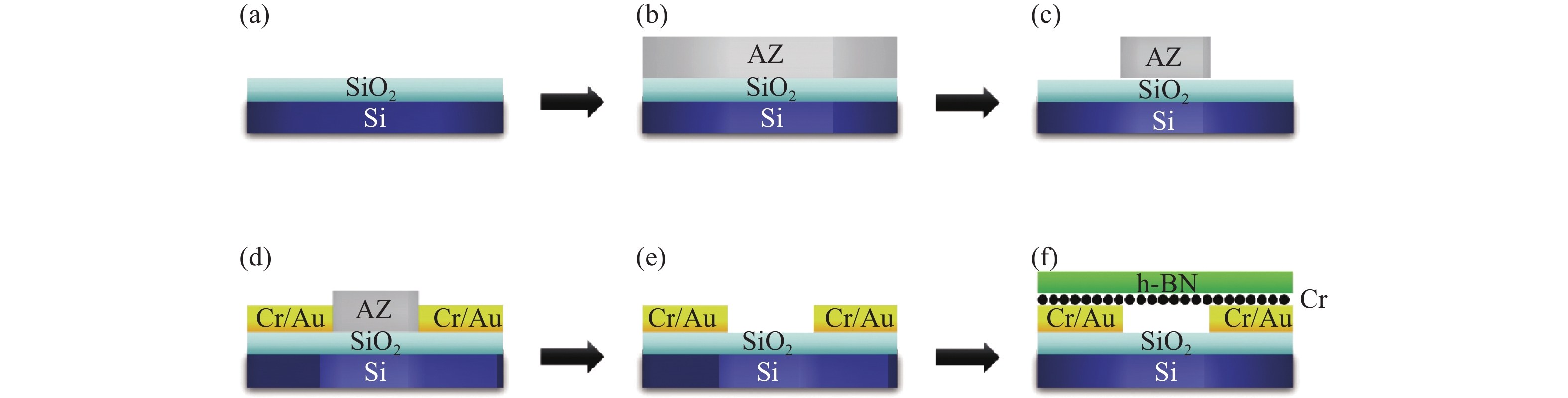
利用紫外光刻、电子束蒸镀、剥离等工艺,笔者在硅片衬底上预先制备好金属电极;通过机械剥离的方法得到单层和少层石墨烯,利用拉曼光谱可以判断石墨烯层数[26]和h-BN的不同厚度;采取干法转移的方式,利用聚二甲基硅氧烷和聚碳酸酯薄膜(PDMS/PC)将h-BN与石墨烯堆叠形成一个范德华异质结,而后精准转移到预制的电极上,形成具有悬空结构的石墨烯器件。器件制备流程如图1所示。

图 1 悬空石墨烯/六方氮化硼异质结器件制备流程示意图。(a)清洗硅片;(b)旋涂AZ光刻胶;(c)光刻图形化AZ光刻胶;(d)蒸镀Cr/Au金属电极;(e)剥离电极;(f)将石墨烯/六方氮化硼异质结直接转移到电极上制备悬空结构器件
Figure 1. Schematic diagram of the fabrication process of suspended graphene/hexagonal boron nitride heterojunction devices. (a) Cleaning the silicon wafer; (b) Spin-coating AZ photoresist; (c) Photolithographic patterning of AZ photoresist; (d) Evaporation of Cr/Au metal electrodes; (e) Lift-off electrodes; (f) Graphene/hexagonal boron nitride heterojunctions are directly transferred to electrodes to prepare suspended structure devices
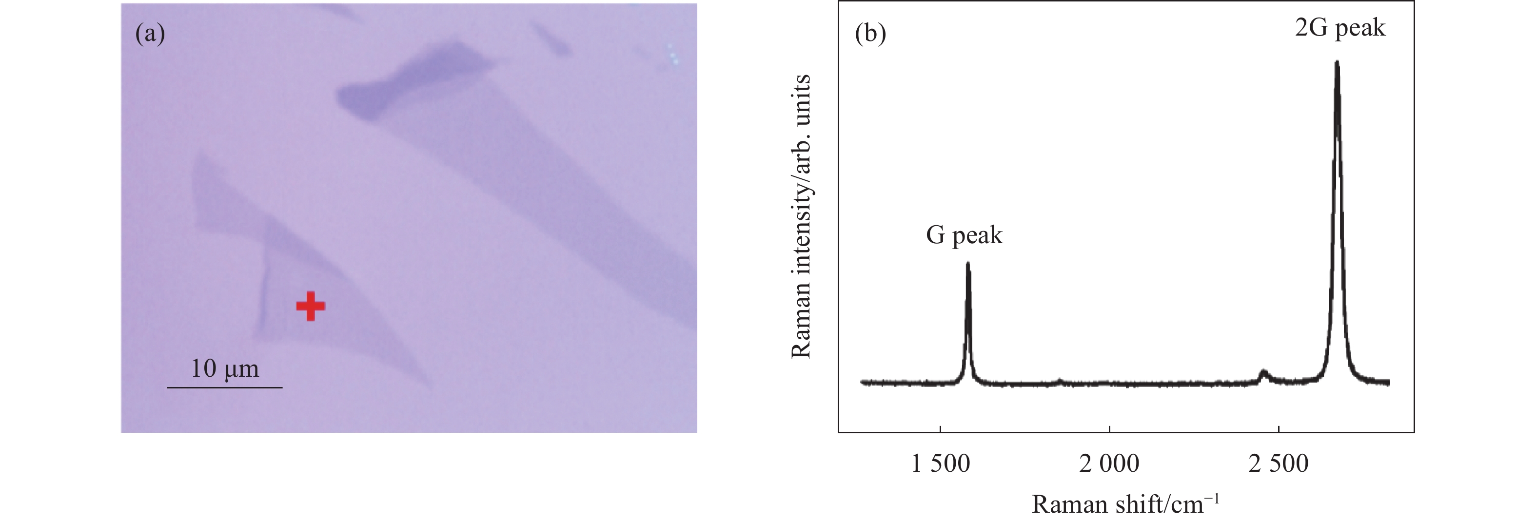
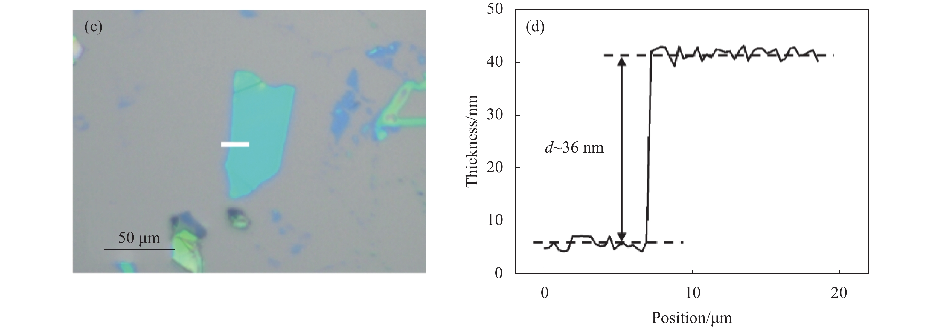
悬空石墨烯器件的制作主要分为3步:(1)制作电极。如图1(a)~(e),在硅片表面旋涂AZ5214光刻胶,经过紫外曝光以及显影后得到所需的电极图案,通过电子束蒸镀工艺在曝光区域蒸镀厚度分别为5 nm的铬(Cr)层和300 nm的金(Au)层,使用剥离工艺将多余的胶去除得到所需的金属电极。为了形成有效的悬空结构,电极的高度为305 nm,高于传统微纳工艺中的30 nm或者50 nm。两电极之间相距4.0 μm,这时两个电极与硅衬底之间构成了一个矩形凹槽作为悬空结构,以便石墨烯/h-BN异质结的悬空;(2)剥离材料。采用机械剥离方法制备所需的石墨烯和h-BN。在光学显微镜下,寻找不同厚度的石墨烯,见图2(a),由于白光的干涉效应,SiO2/Si衬底上的不同层数石墨烯在光学显微镜下显示出不同的颜色和对比度。根据石墨烯拉曼光谱G峰和2D峰的强度,笔者能分辨1~4层石墨烯,图2(b)为对应图2(a)红色十字处的拉曼光谱,由于G峰强度低于2D峰,而且两个峰均为洛伦兹单峰,因此可以判断为单层石墨烯。h-BN的制备和表征与石墨烯类似,如图2(c)所示,不同厚度的h-BN在光学显微镜下的颜色不同,通过原子力显微镜(Atomic force microscopy, AFM)(见图2(d))笔者可以测得图2(c)中h-BN白色横线处的厚度为36 nm;(3)转移h-BN/石墨烯。干法转移h-BN/石墨烯异质结,通过光学显微镜和拉曼光谱确定需要的单层或者少层石墨烯。范德华异质结构的堆叠和转移采用的是基于聚二甲基硅氧烷和聚碳酸酯薄膜(PDMS+PC)的干法转移,即:将转移载体加热到适当温度(90 ℃),利用范德华力将h-BN和石墨烯粘起并堆叠,然后加热PDMS释放PC,实现异质结从硅片到电极上方的转移,最后将样品先后置于氯仿、异丙醇和去离子水中浸泡清洗以去除残留的PC等杂质,完成悬空石墨烯器件的制备。
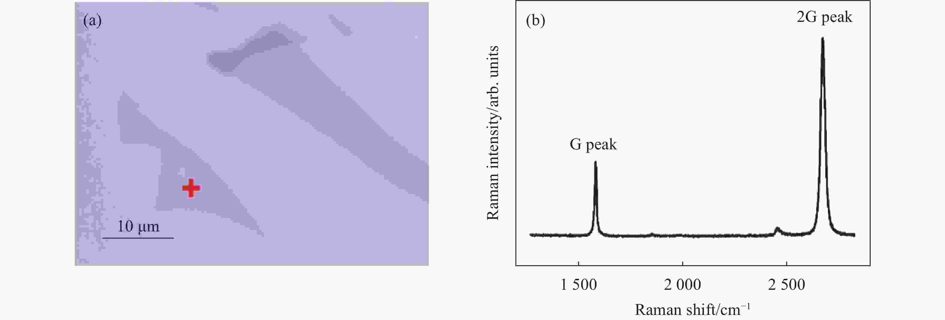
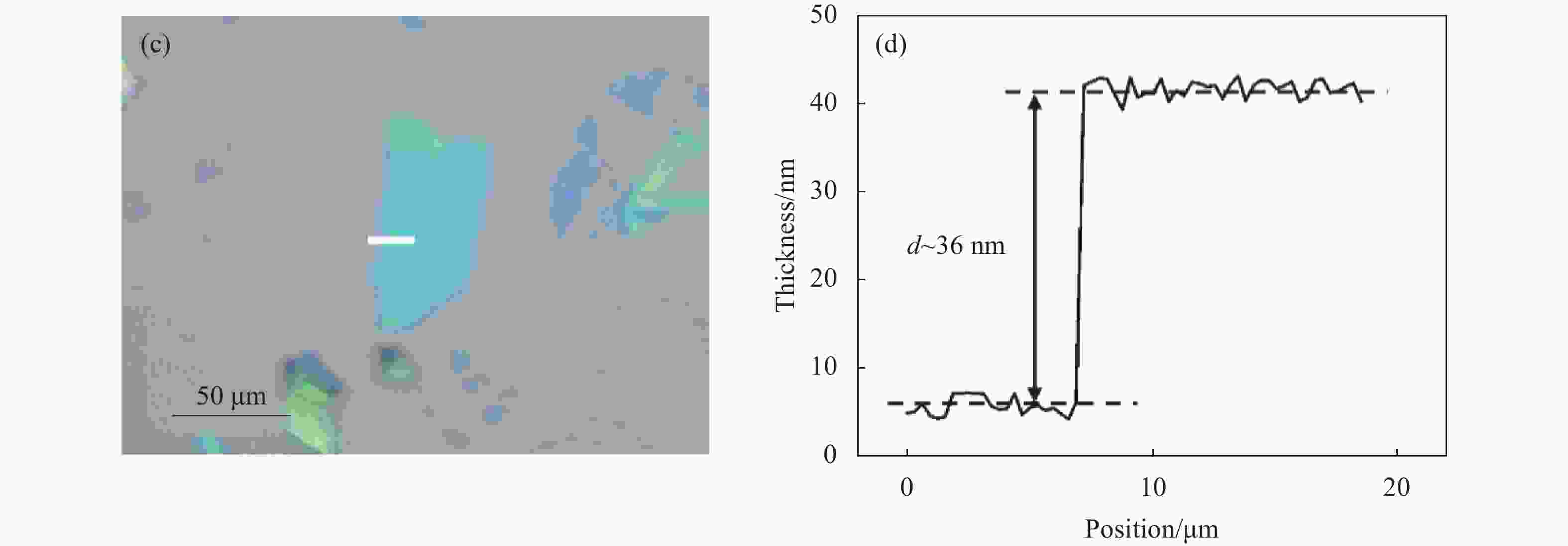
图 2 机械剥离单层石墨烯和多层六方氮化硼的表征。(a)单层石墨烯的光学显微镜照片,红色十字标注了拉曼光谱的聚焦位置;(b)单层石墨烯的拉曼光谱,其中G峰强度明显低于2D峰强度,证明为单层石墨烯;(c)多层六方氮化硼的光学显微镜照片,白色实线标注了原子力显微镜的测量位置;(d)多层六方氮化硼的厚度,约为36 nm
Figure 2. Characterization of mechanically exfoliated monolayer graphene and multilayer hexagonal boron nitride. (a) Optical microscope image of monolayer graphene, the red cross marks the focus position of Raman spectroscopy; (b) Raman spectrum of monolayer graphene, in which the G peak intensity is significantly lower than the 2D peak intensity, proving it is a monolayer graphene; (c) Optical microscope image of a multilayer hexagonal boron nitride, the white solid line marks the measurement position of atomic force microscope; (d) The thickness of multilayer hexagonal boron nitride is about 36 nm
-
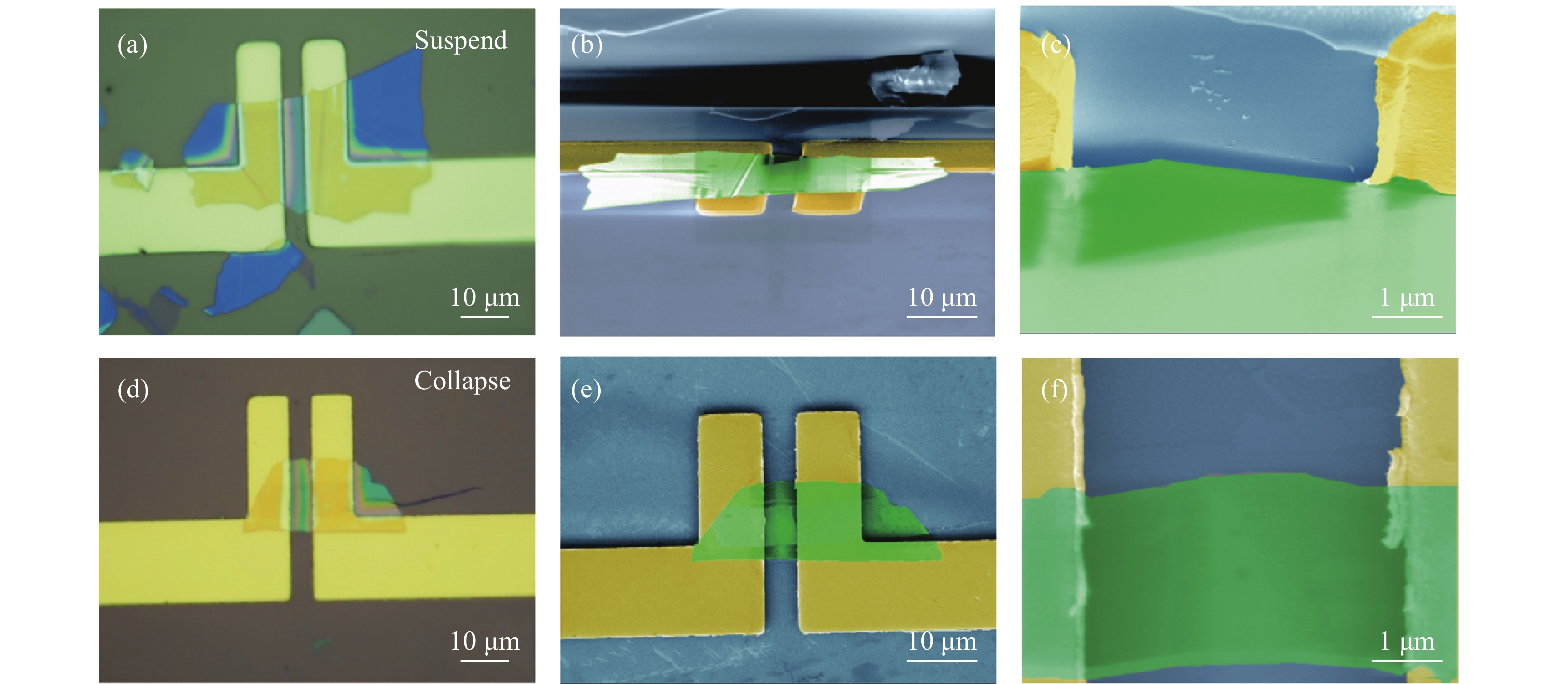
完成器件制备后,首先利用光学显微镜(Optical microscopy,OM)和扫描电子显微镜(Scanning electron microscopy,SEM)表征器件结构。图3(a)~(c)、(d)~(f)分别为悬空的和塌陷的两个石墨烯/h-BN器件的显微镜照片。其中图3(a)和图3(d)分别为50倍放大倍数下两个器件的光学显微镜照片,其余图片为相对应的SEM照片。通过光学显微镜照片,可以判断器件的完整性以及转移后范德华异质结中石墨烯和电极接触的位置,如图3(a)和图3(d)所示,沟道部分异质结颜色可以观察到条纹状变化,这一现象是由于异质结与衬底高度不一致产生了光学薄膜干涉引起的。图3(b)、(e)为低放大倍数下器件整体的SEM照片,图(c)、(f)为高放大倍数下悬空部分细节的SEM照片。根据器件的SEM照片阴影变化,可以判断器件的悬空与塌陷状态,见图3(c),悬空的器件沟道部分异质结的阴影连续均匀。说明,薄层的h-BN在范德华力的作用下,紧密吸附石墨烯,有效地增强了悬空石墨烯的机械力学稳定性,避免了在制备、测试和表征过程中石墨烯由于外部应力(重力、静电力等)而导致的坍塌、断裂和卷曲等失效。此外,致密的h-BN晶体结构可以有效隔绝外部环境对石墨烯的大部分影响,避免污染和掺杂,保证了器件的高质量。
图 3 悬空石墨烯器件的显微镜表征。(a)完成制备流程后悬空的石墨烯器件光学显微镜照片;(b)~(c)悬空石墨烯器件对应不同放大倍数的扫描电子显微镜照片;(d)完成制备流程后坍塌的石墨烯器件光学显微镜照片;(e)~(f)坍塌石墨烯器件对应不同放大倍数的扫描电子显微镜照片
Figure 3. Microscopy characterizations of suspended graphene devices. (a) Optical microscopy image of graphene devices suspended after the completion of the fabrication process; (b)-(c) Corresponding scanning electron microscopy images of different magnifications; (d) Optical microscopy image of graphene devices collapsed after the completion of the fabrication process; (e)-(f) Corresponding scanning electron microscopy images of different magnifications
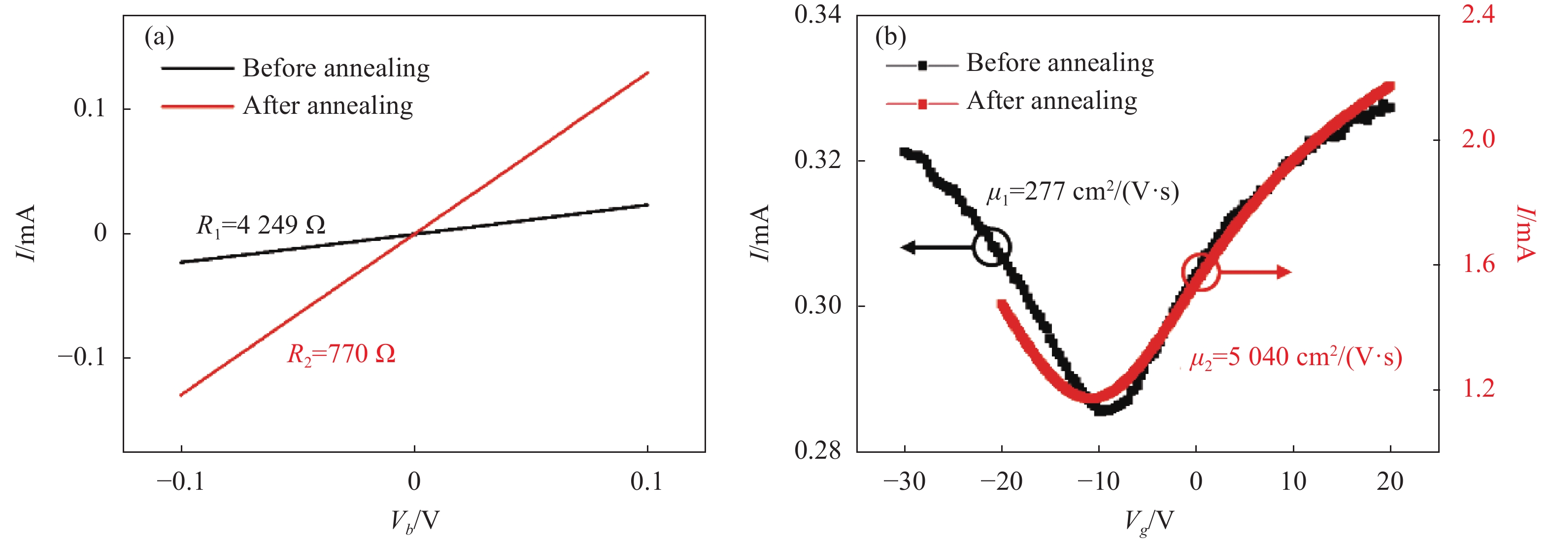
在室温条件下用真空探针台测试器件电学性能。在测试腔达到2.2×10⁻⁵ hPa真空度后,使用源表2636B在源漏极加偏压得到电流电压的输出曲线(I-Vb)以及电阻值,而后固定偏压改变栅压,分别得到0.1 V、0.5 V和1 V偏压下的场效应曲线(I-Vg)。完成退火前器件的电学性能测试之后,将器件置于高真空退火炉进行退火处理。以10 ℃/min的升温速度加热到400 ℃,保温3 h,之后再降温到室温,整个退火操作在4.5×10⁻⁴ hPa的真空度下进行,以防止高温下石墨烯被氧化。退火之后,对器件进行与退火前相同的测试表征,包括光学显微镜观察,探针台电学测试等。对比分析测试结果,计算载流子迁移率,确定器件退火前后的变化。载流子迁移率计算公式为:
$$ \begin{split} \\ \mu =\frac{{{\rm{d}}I}_{b}}{{{\rm{d}}V}_{g}}\cdot \frac{L}{W}\cdot \frac{1}{{C}_{g}\cdot {V}_{b}} \end{split}$$ (1) 式中:$ {I}_{b} $为电流;$ {V}_{g} $为栅极电压;L与W分别为悬空石墨烯的长度与宽度;Vb为偏置电压;Cg为介质电容。
-
退火前后,对同一器件进行了相同的电学测试。得到0 V栅压下的输出特征曲线和0.1 V偏压下的转移特征曲线,如图4所示,黑色为退火前数据,红色为退火后数据。图4(a)为悬空石墨烯焦耳热红外辐射器件的输出特性曲线,偏压变化范围为−0.1~0.1 V,退火前的电阻为4 249 Ω,退火之后电阻减少至770 Ω。图4(b)为器件在0.1 V偏压下的转移特性曲线,根据上述公式(1)计算得到,退火前后悬空石墨烯的迁移率分别为277 cm2/(V·s)和5040 cm2/(V·s),退火后石墨烯的电阻降低到退火前的六分之一,载流子迁移率提高到退火前的18倍。电学测试结果说明高真空热退火可以使石墨烯更好地接触金属电极,同时能有效去除悬空石墨烯器件中大部分的气泡、污染等缺陷,降低接触电阻的同时,提高了石墨烯本身的电导率。

图 4 悬空石墨烯器件退火前后的电学特性比较。(a)退火前后的I-Vb曲线对比;(b)退火前后的场效应I-Vg曲线对比(黑色为退火前,红色为退火后)
Figure 4. Comparison of electrical properties of suspended graphene devices before and after annealing. (a) Comparison of I-Vb curves before and after annealing; (b) Comparison of field effect I-Vg curves before and after annealing (black is before annealing, red is after annealing)
完成退火后的电学测试之后,研究了悬空石墨烯在偏置电压焦耳热作用下的温度特性和红外热辐射特性,其中石墨烯的温度通过拉曼光谱测试得到,而红外热辐射特性则通过发光光谱测试得到。石墨烯拉曼光谱主要的特征峰有G峰和2D峰。其中G峰位于1582 cm−1附近,与温度呈线性相关,当温度升高时,石墨烯G峰位置向低波数方向移动。其关系表达式为[1, 27]:
$$ {\omega }_{G}\left(T\right)={\omega }_{0}+\chi T $$ (2) 式中:$ {\omega }_{G}\left(T\right) $为温度为T时G峰的峰位;$ {\omega }_{0} $为室温(300 K)下G峰的拉曼位移;$ \chi $为一阶温度系数。通过加热真空腔样品台改变悬空石墨烯的环境温度,将温度从室温升至800 ℃,每50 ℃在悬空石墨烯中心点测一次拉曼光谱,得到不同温度下石墨烯G峰峰位。如图5(a)所示,绘制了G峰峰位随外界温度变化的散点图,通过线性拟合得到斜率为−0.0185 cm−1/℃,即为温度系数$ \chi $。

图 5 悬空石墨烯器件在偏压下的拉曼光谱和红外辐射光谱。(a)不同环境温度下石墨烯拉曼G峰位置的变化,红色实线是线性拟合结果;(b)不同偏压下石墨烯拉曼光谱的变化,黑色虚线标注出G峰和2D峰位置的变化;(c)偏压为6 V时,不同聚焦位置的红外辐射光谱,分别为石墨烯(Gr)、六方氮化硼(h-BN)、金电极(Au)和二氧化硅(SiO2);(d)不同偏压下石墨烯的红外辐射光谱,Y轴为对数坐标,X轴为线性坐标
Figure 5. Raman spectra and infrared radiation spectra of suspended graphene devices under bias voltage. (a) Evolution of graphene Raman G peak position at different ambient temperatures, the red solid line is the linear fitting; (b) Evolution of graphene Raman spectrum under different bias voltages, the black dotted line marks the G peak and 2D peak positions; (c) Infrared radiation spectra of different focus positions for graphene (Gr), hexagonal boron nitride (h-BN), gold electrode (Au) and silicon dioxide (SiO2) at a bias voltage of 6 V; (d) Infrared radiation spectra of graphene under different bias voltages, with logarithmic coordinates on the Y axis and linear coordinates on the X axis
完成石墨烯拉曼G峰随环境温度变化的线性拟合后,进行石墨烯器件焦耳热的实验研究。首先石墨烯器件需置于真空腔中避免高温下的氧化失效,而后在器件源漏两端加上偏压,此时悬空石墨烯在偏置电流焦耳热效应的作用下被加热,温度升高,并以黑体辐射的形式向外发射光子。如图5(b)所示,随着偏压从0 V增加到8 V, G峰位置向低波数的方向移动,表明悬空石墨烯的温度升高。根据公式(2)可以推算出8 V偏置电压下的悬空石墨烯中心的温度为836 K。通过发光光谱的测试发现,在偏置电压为6 V时,悬空石墨烯器件辐射光谱出现明显的红外辐射波峰,如图5(c)所示。通过测量悬空器件不同位置(石墨烯中心、二氧化硅衬底、六方氮化硼、金电极)处的辐射光谱发现,Au、SiO2、h-BN的辐射光谱基本重合,而石墨烯的辐射光谱有明显不同的特征峰,从而排除了外界环境的干扰。说明在6 V的偏置电压下,石墨烯温度升高并形成明显的热辐射,通过拉曼光谱计算得到此时石墨烯的温度为645 K。随着偏压的增大,悬空石墨烯热辐射的强度逐渐增强,且向短波长方向移动,如图5(d)所示,在8 V偏压下悬空石墨烯温度升高到836 K,并在波长955 nm处表现出强烈的红外辐射信号。由于悬空石墨烯/氮化硼异质结与硅片衬底构成了一个光学Fabry–Pérot谐振腔(F-P腔),当石墨烯在焦耳热的作用下温度升高并辐射电磁波时,电磁波在腔内经过多次反射透射而相干叠加,导致悬空石墨烯的焦耳热辐射光谱与经典的黑体辐射光谱有所区别。这一现象为进一步通过设计光学微腔和光子晶体等周期性微纳结构实现对石墨烯辐射光谱的有效调控(如1550 nm光通信波段),并构建硅基集成石墨烯纳米光子器件提供了新的思路。
-
文中提出了一种高质量悬空石墨烯焦耳热辐射器件的可控制备新方法,并研究了悬空石墨烯器件的电学特性、温度特性以及热辐射特性。得益于石墨烯和六方氮化硼之间的范德华相互作用,六方氮化硼为悬空石墨烯提供一个良好的支撑悬挂作用,有效提高了悬空石墨烯的机械力学稳定性,避免了其在转移、微纳工艺和测试表征过程中产生塌陷、断裂和卷曲等失效情况,大大提高了悬空石墨烯器件的成品率与综合性能。通过对悬空石墨烯器件进行高真空热退火处理,使得石墨烯和金属电极的贴合更加紧密,减小了接触电阻,同时退火处理也能有效去除悬空石墨烯器件在制备过程中产生的气泡、化学残留物等缺陷,从而大幅提高了石墨烯的载流子迁移率。最后,基于高质量的悬空石墨烯器件,研究了悬空石墨烯在偏压焦耳热作用下的温度特性和红外热辐射特性。结果表明:随着偏压的增大,石墨烯的温度升高,热辐射光谱中心波长发生蓝移。在偏压为8 V时,石墨烯温度达到836 K,并在955 nm处有强烈的近红外辐射信号。这些结果为制备高质量悬空石墨烯以及悬空二维材料器件,深入研究二维材料的本征物理性质,发展基于悬空范德华异质结的红外热辐射器件和纳米机电传感器等新型纳米器件提供了重要的参考价值。
Controllable fabrication and characterization of suspended graphene/hexagonal boron nitride heterostrcuture Joule heating infrared radiation devices (invited)
-
摘要: 石墨烯具有优异的光、电、热以及力学性质,而悬空石墨烯避免了衬底带来的褶皱、载流子散射和掺杂等影响因素,可以充分展现石墨烯的本征物理特性,因此在高性能石墨烯微电子和光电子器件研究中具有重要意义。然而,目前悬空石墨烯器件还存在着制备方法复杂、成品率低、性能不稳定等挑战。文中提出了一种利用六方氮化硼吸附石墨烯,将其定点转移到金属电极,制备悬空石墨烯焦耳热红外辐射器件的新方法。六方氮化硼对悬空石墨烯具有良好的支撑悬挂作用,有效提高了悬空石墨烯的力学稳定性,避免了坍塌、断裂等失效情况。真空热退火处理后悬空石墨烯的电阻降低到退火处理前的约六分之一,载流子迁移率比退火前提高了约18倍。当偏置电压为8 V时,拉曼光谱测试发现石墨烯温度为836 K,器件在955 nm波长处表现出强烈的红外辐射信号。Abstract:
Objective Graphene exhibits superior optical, electrical, thermal, and mechanical properties, while the suspended structure avoids external factors such as wrinkles, carrier scattering and doping caused by rough substrates, and can maximize the intrinsic physical properties of graphene, which is of great significance in the research of high-performance graphene microelectronics and optoelectronic devices. However, the current research on suspended graphene devices is yet limited by the complicated fabrication methods, low yield, and unstable electrical and thermal properties of devices. Methods In order to improve the yield rate of suspended graphene nano devices and the comprehensive performance of the device, this paper develops a method by using two-dimensional material hexagonal boron nitride (h-BN) to pick up graphene, then transfers graphene directly to the surface of pre-fabricated metal electrodes, and finally prepares suspended graphene Joule heating infrared radiation devices (Fig.1). In order to further reduce the defects and improve the device quality, a high-vacuum thermal annealing treatment was performed on the suspended graphene device. Based on the high-quality suspended graphene device after annealing, we used Raman spectroscopy and luminescence spectroscopy to study the temperature characteristics and thermal radiation spectral characteristics of the device under the Joule heating effect caused by bias voltage. Result and discussion The experimental results show that the h-BN covers the upper surface of the graphene and plays a critical role in supporting and suspending the graphene, which effectively improves the stability of the suspended graphene and avoids device failures such as collapse and fracture. After the thermal annealing at 400 ℃/3 h in high vacuum of 4.5×10⁻⁴ hPa, the resistance of suspended graphene decreased to one-sixth of that before annealing, and the carrier mobility increased eighteen times compared with that before annealing (Fig.4). When the bias voltage is 8 V, the temperature of suspended graphene measured by Raman spectroscopy is 836 K, and it shows a strong infrared radiation signal at 955 nm wavelength (Fig.5). Conclusions This paper presents a controllable fabrication method of high-quality suspended graphene Joule heating radiation devices, and investigates the electrical, temperature, and thermal radiation characteristics of suspended graphene devices. The h-BN in the device structure demonstrates a good support and adhesion effect for suspended graphene, which greatly improves the device performance. The impurities attached to the surface of graphene can be effectively removed through high vacuum thermal annealing, which greatly improves the electrical performance of suspended graphene devices. It was observed that the temperature of graphene increased with the increase of bias voltage, showing a blue shift in the Raman spectrum and strong thermal radiation emission. The research results of this paper provide an important reference for deepening the understanding of the intrinsic physical properties of suspended graphene and developing optoelectronic applications based on suspended graphene devices. -
图 1 悬空石墨烯/六方氮化硼异质结器件制备流程示意图。(a)清洗硅片;(b)旋涂AZ光刻胶;(c)光刻图形化AZ光刻胶;(d)蒸镀Cr/Au金属电极;(e)剥离电极;(f)将石墨烯/六方氮化硼异质结直接转移到电极上制备悬空结构器件
Figure 1. Schematic diagram of the fabrication process of suspended graphene/hexagonal boron nitride heterojunction devices. (a) Cleaning the silicon wafer; (b) Spin-coating AZ photoresist; (c) Photolithographic patterning of AZ photoresist; (d) Evaporation of Cr/Au metal electrodes; (e) Lift-off electrodes; (f) Graphene/hexagonal boron nitride heterojunctions are directly transferred to electrodes to prepare suspended structure devices
2 机械剥离单层石墨烯和多层六方氮化硼的表征。(a)单层石墨烯的光学显微镜照片,红色十字标注了拉曼光谱的聚焦位置;(b)单层石墨烯的拉曼光谱,其中G峰强度明显低于2D峰强度,证明为单层石墨烯;(c)多层六方氮化硼的光学显微镜照片,白色实线标注了原子力显微镜的测量位置;(d)多层六方氮化硼的厚度,约为36 nm
2. Characterization of mechanically exfoliated monolayer graphene and multilayer hexagonal boron nitride. (a) Optical microscope image of monolayer graphene, the red cross marks the focus position of Raman spectroscopy; (b) Raman spectrum of monolayer graphene, in which the G peak intensity is significantly lower than the 2D peak intensity, proving it is a monolayer graphene; (c) Optical microscope image of a multilayer hexagonal boron nitride, the white solid line marks the measurement position of atomic force microscope; (d) The thickness of multilayer hexagonal boron nitride is about 36 nm
图 3 悬空石墨烯器件的显微镜表征。(a)完成制备流程后悬空的石墨烯器件光学显微镜照片;(b)~(c)悬空石墨烯器件对应不同放大倍数的扫描电子显微镜照片;(d)完成制备流程后坍塌的石墨烯器件光学显微镜照片;(e)~(f)坍塌石墨烯器件对应不同放大倍数的扫描电子显微镜照片
Figure 3. Microscopy characterizations of suspended graphene devices. (a) Optical microscopy image of graphene devices suspended after the completion of the fabrication process; (b)-(c) Corresponding scanning electron microscopy images of different magnifications; (d) Optical microscopy image of graphene devices collapsed after the completion of the fabrication process; (e)-(f) Corresponding scanning electron microscopy images of different magnifications
图 4 悬空石墨烯器件退火前后的电学特性比较。(a)退火前后的I-Vb曲线对比;(b)退火前后的场效应I-Vg曲线对比(黑色为退火前,红色为退火后)
Figure 4. Comparison of electrical properties of suspended graphene devices before and after annealing. (a) Comparison of I-Vb curves before and after annealing; (b) Comparison of field effect I-Vg curves before and after annealing (black is before annealing, red is after annealing)
图 5 悬空石墨烯器件在偏压下的拉曼光谱和红外辐射光谱。(a)不同环境温度下石墨烯拉曼G峰位置的变化,红色实线是线性拟合结果;(b)不同偏压下石墨烯拉曼光谱的变化,黑色虚线标注出G峰和2D峰位置的变化;(c)偏压为6 V时,不同聚焦位置的红外辐射光谱,分别为石墨烯(Gr)、六方氮化硼(h-BN)、金电极(Au)和二氧化硅(SiO2);(d)不同偏压下石墨烯的红外辐射光谱,Y轴为对数坐标,X轴为线性坐标
Figure 5. Raman spectra and infrared radiation spectra of suspended graphene devices under bias voltage. (a) Evolution of graphene Raman G peak position at different ambient temperatures, the red solid line is the linear fitting; (b) Evolution of graphene Raman spectrum under different bias voltages, the black dotted line marks the G peak and 2D peak positions; (c) Infrared radiation spectra of different focus positions for graphene (Gr), hexagonal boron nitride (h-BN), gold electrode (Au) and silicon dioxide (SiO2) at a bias voltage of 6 V; (d) Infrared radiation spectra of graphene under different bias voltages, with logarithmic coordinates on the Y axis and linear coordinates on the X axis
-
[1] Calizo I, Balandin A A, Bao W, et al. Temperature dependence of the Raman spectra of graphene and graphene multilayers [J]. Nano Letters, 2007, 7(9): 2645-2649. doi: 10.1021/nl071033g [2] Berciaud Stéphane, Han Melinda Y, Mak Kin Fai, et al. Electron and optical phonon temperatures in electrically biased graphene [J]. Physical Review Letters, 2010, 104(22): 227401. doi: 10.1103/PhysRevLett.104.227401 [3] Kim Young Duck, Gao Yuanda, Shiue Ren-Jye, et al. Ultrafast graphene light emitters [J]. Nano Letters, 2018, 18(2): 934-940. doi: 10.1021/acs.nanolett.7b04324 [4] Yang Qi, Shen Jun, Wei Xingzhan, et al. Recent progress on the mechanism and device structure of graphene-based infrared detectors [J]. Infrared and Laser Engineering, 2020, 49(1): 0103003. (in Chinese) [5] Liu Zhi, Chen Jimin, Li Dongfang, et al. Laser-induced transformation of carbon nanotubes into graphene nanoribbons and their conductive properties [J]. Infrared and Laser Engineering, 2020, 49(9): 20200298. (in Chinese) [6] Geim A K, Novoselov K S. The rise of graphene [J]. Nature Materials, 2007, 6(3): 183-191. [7] Bae Myungho, Ong Zhunyong, Estrada David, et al. Imaging, simulation, and electrostatic control of power dissipation in graphene devices [J]. Nano Letters, 2010, 10(12): 4787-4793. [8] Freitag Marcus, Steiner Mathias, Martin Yves, et al. Energy dissipation in graphene field-effect transistors [J]. Nano Letters, 2009, 9(5): 1883-1888. [9] Freitag Marcus, Chiu Hsin-Ying, Steiner Mathias, et al. Thermal infrared emission from biased graphene [J]. Nature Nanotechnology, 2010, 5(7): 497-501. [10] Mahlmeister N H, Luxmoore I J, Poole T, et al. Thermal emission from large area chemical vapor deposited graphene devices [J]. Applied Physics Letters, 2013, 103(13): 131901-131906. [11] Kim Young Duck, Kim Hakseong, Cho Yujin, et al. Bright visible light emission from graphene [J]. Nature Nanotechnology, 2015, 10(8): 676-681. [12] Tchon K, Go Ral I. Graphene hot-electron light bulb: Incandescence from hBN-encapsulated graphene in air [J]. 2D Materials, 2018, 5(1): 1910-1915. [13] Shiue Ren-Jye, Gao Yuanda, Tan Cheng, et al. Thermal radiation control from hot graphene electrons coupled to a photonic crystal nanocavity [J]. Nature Communications, 2019, 10 (1): 109. [14] Luo Fang, Fan Yansong, Peng Gang, et al. Graphene thermal emitter with enhanced joule heating and localized light emission in air [J]. ACS Photonics, 2019, 6(8): 2117-2125. [15] Brar Victor W, Sherrott Michellez, Jang Min Seok, et al. Electronic modulation of infrared radiation in graphene plasmonic resonators [J]. Nature Communications, 2015, 6 (1): 7032. [16] Meyer Jannik C, Geim A K, Katsnelson M I, et al. The structure of suspended graphene sheets [J]. Nature, 2007, 446: 60-63. [17] Fischbein Michael D, Drndic Marija. Electron beam nanosculpting of suspended graphene sheets [J]. Condensed Matter, 2008, 93(11): 113107. [18] Alyobi Mona, Barnett Chris, Cobley Richard. Effects of thermal annealing on the properties of mechanically exfoliated suspended and on-substrate few-layer graphene [J]. Crystals, 2017, 7(11): 349. doi: 10.3390/cryst7110349 [19] Li Qiang, Cheng Zengguang, Li Zhongjun. Fabrication of suspended graphene devices and their electronic properties [J]. Chinese Physics B, 2010, 19(9): 97307. [20] Watanabe Kenji, Taniguchi Takashi, Kanda Hisao. Direct-bandgap properties and evidence for ultraviolet lasing of hexagonal boron nitride single crystal [J]. Nature Materials, 2004, 3(6): 404-409. [21] Cassabois G, Valvin P, Gil B. Hexagonal boron nitride is an indirect bandgap semiconductor [J]. Nature Photonics, 2016, 10(4): 262-266. doi: 10.1038/nphoton.2015.277 [22] Wang L, Meric I, Huang P Y, et al. One-dimensional electrical contact to a two-dimensional material. [J]. Science, 2013, 342: 614-617. [23] Dean C R, Young A F, Meric I, et al. Boron nitride substrates for high-quality graphene electronics [J]. Nature Nanotechnology, 2010, 5(10): 722-726. [24] Gao Xin, Zheng Liming, Luo Fang, et al. Integrated wafer-scale ultra-flat graphene by gradient surface energy modulation [J]. Nature Communications, 2022, 13(1): 5410. [25] Fukamachi Satoru, Solís-fernández Pablo, Kawahara Kenji, et al. Large-area synthesis and transfer of multilayer hexagonal boron nitride for enhanced graphene device arrays [J]. Nature Electronics, 2023, 6(2): 126-136. [26] Li Xiaoli, Qiao Xiaofen, Han Wenpeng, et al. Layer number identification of intrinsic and defective multilayered graphenes up to 100 layers by the raman mode intensity from substrates [J]. Nanoscale, 2015, 7(17): 8135-8141. [27] Zhang T Y, Wang H W, Xia X X, et al. A monolithically sculpted van der waals nano-opto-electro-mechanical coupler [J]. Light Sci Appl, 2022, 11(1): 76-85. -

 点击查看大图
计量
- 文章访问数: 207
- HTML全文浏览量: 47
- PDF下载量: 31
- 被引次数: 0

