


 下载:
下载:


-
随着集成电路制造按摩尔定律发展,半导体器件的制备工艺不断进步,单位面积上的晶体管数量越来越多,芯片中器件的体积越来越小,芯片的制作难度和复杂程度也随之提升,因此半导体集成电路制造的退火工艺技术也在不断改进。
以金属氧化物半导体场效应晶体管(MOSFET)为例,其源漏区域的离子掺杂是通过离子注入将杂质原子加速形成高能离子束轰击待改性材料表面。在离子注入的过程中,激烈的碰撞使得被注入材料的晶格遭到破坏,出现大量晶格缺陷,而且随着离子注入剂量增多,晶格损伤也会越大,过多的晶格缺陷会导致器件的性能下降。为了获得更高性能的器件,通常会使用退火工艺消除缺陷并对杂质进行激活[1-7]。但是,随着器件尺寸不断缩小,传统的炉式退火等退火技术已经不能适应芯片制造工艺的要求,退火技术和工艺参数需要不断改进以适应器件尺寸变小带来的技术挑战,这为激光退火进入半导体集成电路制造提供了机会。
脉冲激光退火可以在极短的时间内对材料的特定区域进行照射,被照射的特定区域材料表面吸收激光的能量之后,温度上升融化,并在随后的降温过程中自然地在熔化层液相外延生长出晶体薄膜,这个过程能够重构融化层的晶体结构,同时掺杂也会重新分布溶解于晶体中,达到消除缺陷激活掺杂的目的[8-16]。目前已有多种脉冲激光用于半导体工艺中,
纳秒脉冲激光热退火在20世纪后期成功引入半导体器件制造,用于大批量制造敏感的3D架构器件,如垂直硅基绝缘栅双极晶体管、基于SiC基的垂直功率二极管和背面照明互补金属氧化物半导体(CMOS)成像传感器。目前正在被集成到下一代CMOS和存储器制造的关键退火工艺中[17-29]。
半导体制造领域的激光加工和脉冲激光退火的很多研究采用了不同种类的固体激光[30-37]。总体来说,脉宽越短的脉冲激光越有利于控制热预算,因此,近年来国内外对皮秒、飞秒的超短脉冲固体激光对半导体材料相互作用的研究较多。就激光波长而言,波长短有利于更精确地控制退火范围和效果,但是目前的固体激光波长大多数在红外和可见区域。
准分子激光作为纳秒脉冲的紫外激光,波长短、脉宽较窄,对材料的穿透深度较小,尤其是硅等半导体材料对准分子激光的吸收率较高。此外,聚焦或投影时分辨率高、单脉冲能量大等特点,便于根据应用场景的不同,以部分脉冲能量作为代价对脉冲光斑能量分布进行整形处理。以上特点使得准分子激光在半导体制造的退火技术上具有一定的优势[38]。文中主要调研分析了准分子激光退火应用于半导体集成电路制造的研究进展。
-
图1所示为采取不同退火技术的热预算演化图。不同技术的对比点在于退火的时间窗口与相应的退火峰值温度,更好地控制这两个目标能够更加精确地控制热预算,最终实现材料性能的改善。从炉内退火到单片晶圆快速退火工艺(RTP)和尖峰退火,通过缩短热退火时间窗口来控制退火效果,尤其是实现从材料表面到材料内部温度梯度的控制,本身就具有一系列的挑战。如今亚微秒激光退火研究取得了一系列研究结果[39-40]。
在基于降低热预算的激光退火研究上,K. Huet[41]等人从纳秒激光退火的模拟、激光退火在CMOS接触模块的应用、激光退火在先进互联上的应用和激光退火在3D结构上的应用做了比较详细的总结和分析。
在纳米激光退火的模拟方面,K. Huet等人整理了部分有关激光对硅锗材料进行退火处理模拟的研究结果,指出精确的数值模拟是推动突破性工艺应用的关键。在此基础上,K. Huet等人宣称开发了专门对一维、二维和三维结构激光退火进行模拟的计算工具[42],该工具能够对仿真结构和设备参数进行设置,对参数批量处理和跟踪以及自动生成报告,可用于估计给定目标在制造流程中的最佳激光退火工艺插入点,并评估工艺参数(如激光能量密度、脉冲持续时间、辅助加热温度)和结构特征(如形状、堆叠、材料、掺杂浓度)对退火动力学的影响。
针对激光退火在改善CMOS接触模块(contact module)特性方面的应用已有很多研究成果,如激光退火在层结构[43-47]、图案结构[48-50]、FinFet结构[51]、以及纳米线结构[52-55] 等器件的应用。K. Huet等人对这些研究的分析总结表明,尽管这四种结构从简单到复杂,但在逻辑上研究方法十分类似,其最终目的都是为了了解激光与材料不同结构的相互作用,最终在器件上得到应用,优化工艺,完成更复杂的集成,获得更高性能的器件。
上述研究主要针对接触电阻,希望通过优化参数达到降低电阻的目的,研究结果也证实了激光退火能够达到降低电阻的目的。
图2所示为不同能量密度激光对Ge层结构Ge薄膜退火的SIMS图。在部分熔化和全熔化剖面中,Ge界面仍然存在,但Ge在熔层内重新分布,在近表面处浓度较高,在最大熔体深度附近有一些损耗,这是典型的偏析现象[43],在图案结构中也被证明。

图3对比了非激光退火和激光退火情况之间的接触电阻率变化,清楚地表明了激光退火方法的内在优势及其对finFET器件的适用性[51]。
纳米线结构器件的研究结果表明,激光退火后亚熔化条件下高温区位于表面附近,在更深的区域,由于下面的Ge外延层具有很高的导热性,温度下降得非常快(图4)。这是由于激光退火的吸收效率非常高,大部分发生在表面区域层,只有一小部分被栅和沟道吸收,在退火过程中,该区域产生的热量可以扩散到有价值的的掺杂剂活化区域[54-55]。
激光退火在先进互联的应用上,接触孔和导电线路尺寸缩小以及互联密度不断增长是目前后道工序需亟待解决的问题,而其中对高效低热预算的材料进行改进是解决该问题的关键[56]。对14 nm FinFET中所使用的熔体激光退火工艺流程研究结果见图5。

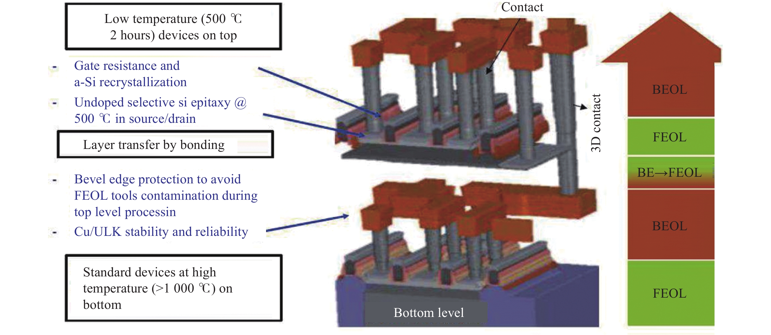
在器件尺寸不断变小的条件下,不论是前道工序(front-end-of-line:FEOL)器件的微缩,还是后道工序(back-end-of-line:BEOL)中接触点和连线的工艺改进都面临技术挑战。激光退火在3D结构器件的研究方面,其主要研究成果集中在三维顺序集成的多晶硅晶化和存储器多晶硅插头形成方面。图6描述了3D顺序集成与其面临的问题。
三维顺序集成主要挑战的是在顶层实现高性能晶体管,同时不降低底层晶体管的电气性能,并将后道工序夹层的热预算保持在500 ℃以下[57]。在过去几年的研究中,激光退火对3D顺序集成的兼容性通过仿真和真实结构得到了验证[58]。在原位掺杂非晶层中结晶并使用激光退火激活掺杂剂能够获得高活化率和大晶粒的充分再结晶,且不影响后道工序[59]。此外,通过化学-机械整平解决结晶后,局部晶界引起的表面粗糙度问题是成功集成激光退火工艺的关键[60]。
在存储器领域,3D NAND通道形成的情况下,由于晶粒尺寸增加和界面缺陷固化,可以观察到存储性能的明显改善。然而随着DRAM阵列晶体管尺寸的不断缩小,接触区域的多晶硅沉积填充可能会出现一些空隙或接缝,这可能会影响接触电阻率,从而影响DRAM操作的整体性能。而研究结果证实激光诱导多晶硅熔解回流是一种有效解决该问题的方法[61-64]。
-
自摩尔定律被提出以来,电路的集成度能够飞速提升的一个重要原因是使用的金属氧化物半导体场效应晶体管(MOSFET)依照按比例缩小理论不断缩小。但事实上,按比例缩小的技术偏离了理想恒定电场规则,当MOSFET器件缩小到一定程度时,晶体管就遇上了短沟道效应阻碍。为了能够突破按比例缩小理论恒定电场的基本限制,人们引入了另一个方案:恒定电压下的按比例缩小。这需要器件缩小时增加掺杂浓度,使得在电压保持不变的前提下增强电场,这又导致强电场击穿器件的可能性增大,同时加剧了短沟道效应。现在人们使用的按比例缩小技术采用了恒定电场和恒定电压相结合的方式,为了防止击穿和短沟道效应,必须严格控制掺杂的横向和纵向扩散。激光退火是一个重要选择。
与传统的快速热退火相比,脉冲激光退火可以在Si中形成超浅结。在足够的能量密度下,脉冲激光退火会导致Si样品中一个明确区域的熔化,掺杂原子均匀地重新分布,且照射后快速凝固过程中发生的非平衡偏析增强了掺杂原子的俘获,有利于高密度掺杂。
La Magna[65]等采用相场法模拟了准分子激光退火(ELA excimer laser annealing)过程中的热场和掺杂浓度的演化过程。
La Magna进行了50 nm的a-Si层和3 nm的SiO2层堆栈于c-Si衬底经受单次ELA脉冲退火的模拟,设置初始温度为450 ℃的均匀热场,激光参数为波长308 nm,脉冲持续时间28 ns。图7所示为熔化和凝固阶段的模拟结果,图8所示为密度场演化图。在熔化过程中,相边界在a-Si区域比在c-Si区域移动得更快。由于两种材料的热性质的变化,相边界在到达a-Si和c-Si边界时速度降低。凝固阶段的特征是除在SiO2/Si界面处和最大熔体深度,其他位置边界速度几乎恒定,且杂质只在液相中扩散,在固相中扩散率很低。


La Magna等人还注意到,模拟中只有前几个脉冲的化学剖面有显著差异。因此,他们对表面处理时所需的照射次数进行预测,认为只需要几个合适能量密度的脉冲就足以达到最佳激活效果。在之后的实验中,对两个和五个脉冲照射的样品的扩散电阻分布测量结果显示,在对应条件下可以获得很高的掺杂激活效率,证实了模拟预测的有效性。同时,La Magna等人还将模拟剖面与实验SIMS剖面进行了对比,如图9所示。这样的比较表明其实验和模拟之间有可靠的一致性。

Fortunato G [66]等建立了一个考虑熔体深度、熔体时间和界面速度的模型来解释在激光脉冲下掺杂在熔化和再生长过程中的行为。其所设置的激光脉冲波长为308 nm,并假设每次脉冲后达到的熔体深度可以呈高斯分布,在平均值附近随机变化。模拟结果表明,在低于热力学极限的条件下,通过准分子激光退火后,Si中形成的掺杂分布是激光退火过程的固有性质,受扩散方程和熔体深度的控制,且只有在一定能量剂量范围内,扩散机制才会出现内在剂量依赖性。同时,对于低于热力学极限的原子浓度水平,Fortunato G等还证明了实验数据可以可靠地与模型相拟合。图10为当衬底温度为450 ℃时,激光照射在Si中形成的熔体深度随激光能量密度变化的函数模拟图。

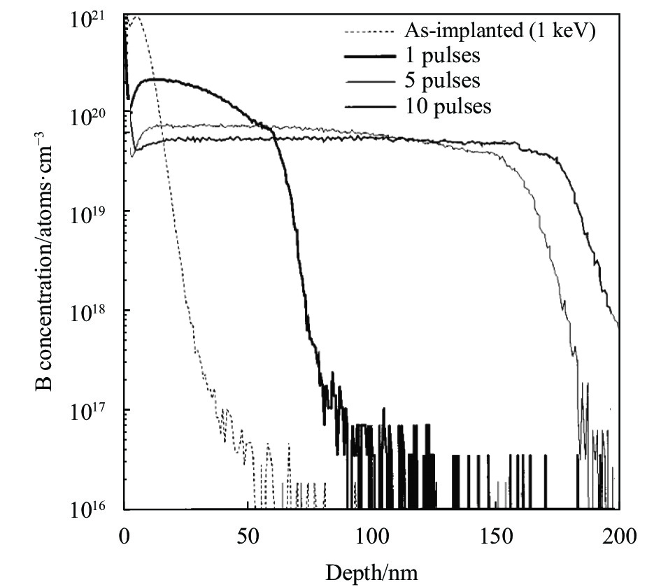
因为硼离子会在退火时产生沟道效应和瞬时增强扩散,所以硼离子注入的p+/n超浅结更难形成。Chong Y F[67]等通过实验表明,利用248 nm的准分子激光可以获得硼掺杂的超浅结。在预非晶化注入的方案下对比准分子激光退火和尖峰退火如图11所示,248 nm的准分子激光退火后的样品结深达到37 nm,相比尖峰退火的样品结深少至少20 nm。Chong Y F等对此的解释为预非晶化层可以在不熔化底层Si的情况下被熔化,当光子在Si衬底的顶表面区域被吸收后,在不到1 ns的时间内,光子的能量被转移到晶格中时,熔解就发生了。由于硼在液相中的扩散率比在固态中的扩散率高约八个数量级,硼原子在熔体深度内几乎均匀地重新分布,从而形成一个突变结。为了说明准分子激光退火对硼扩散深度具有一定控制能力,Chong Y F等还对比了不同脉冲数的扩散深度,如图12所示。

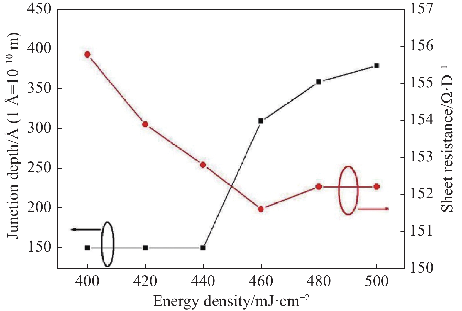
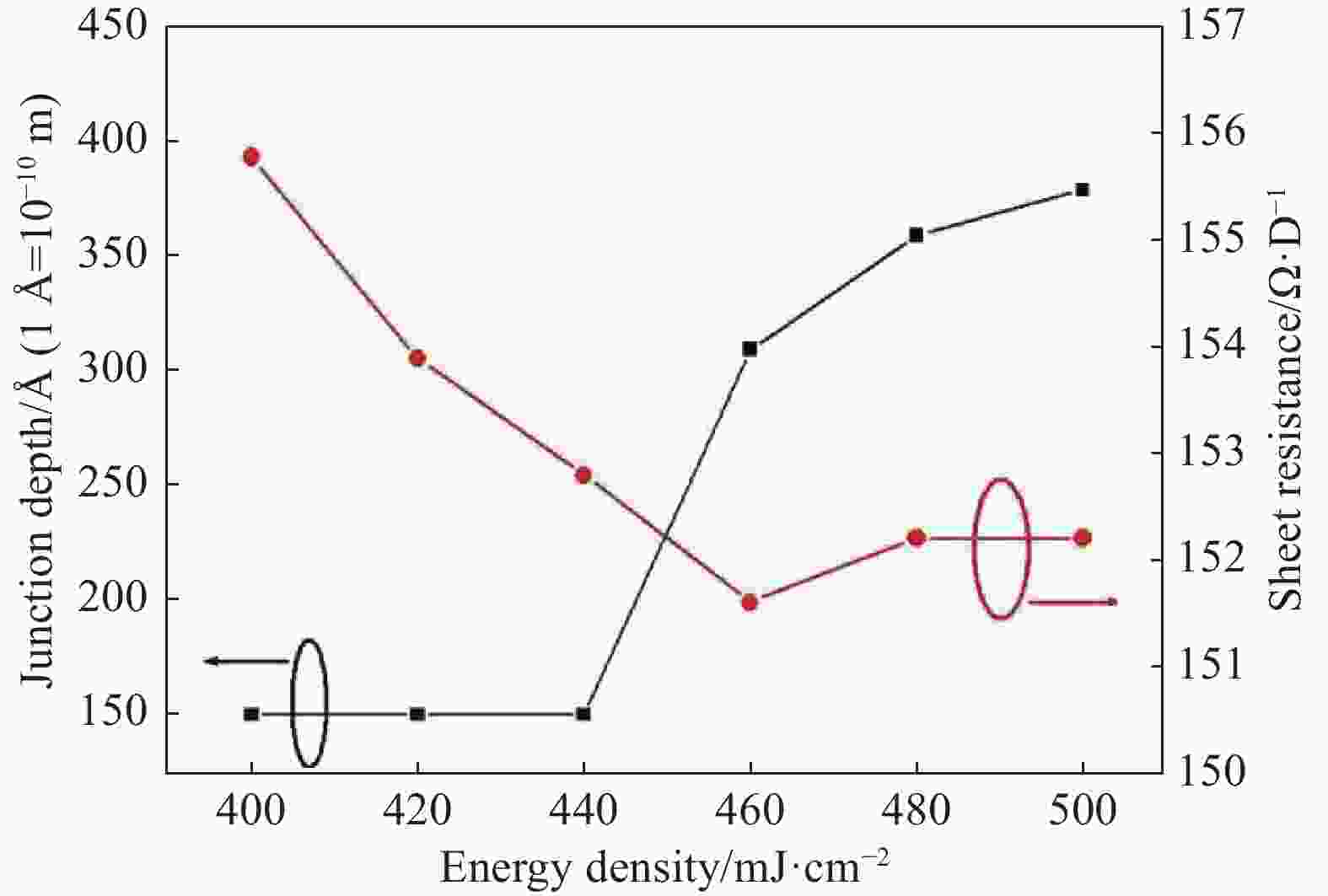
Seung-Woo Do[68]等使用重复频率为50 Hz、照射时间为20 ms、能量密度为400~500 mJ/cm2的ArF (193 nm)准分子激光对磷离子注入的超浅结CMOS器件进行了激光退火研究。如图13所示,当准分子激光能量密度低于440 mJ/cm2时形成的结深几乎相同。将激光能量密度提高到500 mJ/cm2,将结深提高到40 nm,此时能量的提高并没有使结发生显著的变化。当激光能量密度设置为460 mJ/cm2时,可以获得30 nm的浅结。
如图14所示,通过比较双晶X射线衍射(DXRD)曲线,经过准分子激光处理的样品具有更尖锐的峰,说明经过准分子激光处理的掺杂样品缺陷比仅掺杂未经过准分子激光处理的样品更少。
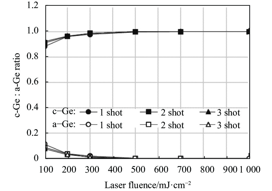
Aid S R[69]等使用KrF准分子激光对磷掺杂的Ge衬底MOS器件进行了激光退火研究,当衬底在500~1000 mJ/cm2之间退火时,可获得较低的电阻。他们通过电阻值估计掺杂激活,通过测定拉曼光谱峰拉曼光谱分析了损伤注入层的再结晶情况,证明所有退火点都发生了再结晶。图15为退火样品的拉曼光谱c-Ge∶a-Ge比值图。根据c-Ge和a-Ge的比值,分析出在高能注入下较低的激光能量密度和脉冲数不能使注入样品完全再结晶,说明低能量激光热退火不能完全修复离子注入造成的损伤。当样品在大于500 mJ/cm2的激光能量密度下退火时,100%的c-Ge拉曼比证实了完全再结晶。由于不同脉冲次数对表面形貌的影响无显著性差异,为了保持重叠退火区域的均匀性,最终他们确定能量密度700 mJ/cm2,二次脉冲作为最佳参数。
Toshiyuki Tabata[70]等使用XeCl准分子激光对锑掺杂的硅衬底MOS器件进行了激光退火研究。图16为锑原子在准分子激光退火前后的SIMS曲线图。当注入锑的硅外延层受到激光照射发生熔融时,锑原子发生像表面强烈偏析。当增加激光能量密度,这种表面偏析会增强,非平衡偏析系数随着辐照激光能量密度的改变有很大变化。此外,当Si外延层几乎完全熔融时,激光退火后活性掺杂水平会显著提高,约为平衡固溶极限的2~4倍。

为了制备出性能更好的器件,应变硅技术和绝缘体上硅技术(silicon on insulator, SOI)也被引入到制程当中。应变硅技术是指通过使应变材料产生引向器件沟道的应力,改变沟道中材料导带或价带的能带结构,来增强载流子迁移率和提高器件速度的技术。SOI在硅晶体管之间利用嵌入或键和的方法形成埋层氧化物隔离顶层硅薄膜层和硅衬底,来降低寄生电容。SOI材料相比体硅具有许多优点,如:隔离集成电路中的元器件,减小集成电路中的寄生电容,消除CMOS电路中的寄生闩锁效应。在处理高性能顶层晶体管的同时需要保持底层晶体管的性能。
2002年,Seong-Dong Kim[71]等利用非晶态硅层的熔化温度比晶态硅层低约300 ℃的条件,结合激光退火和预非晶注入工艺,降低激光器对器件的能量通量,在亚100 nm SOI CMOS的工艺集成上实现了理想的盒形(BOX)超浅结,其中使用参数为脉冲宽度20 ns、波长308 nm的XeCl激光器,SIMS测量激光退火和预非晶注入工艺处理过的器件中硼和砷掺杂曲线如图17所示。Seong-Dong Kim等推断,在非晶硅层开始熔解时存在一个激光能量阈值,低能量单脉冲不足以完全熔化非晶硅层或使掺杂剂充分扩散。与单发高能激光相比,多发辐照增加的激光能量可以在非晶硅层上积累更有效的热能,使熔解深度达到非晶硅/晶硅的初始界面,直到非晶层温度接近晶硅层熔点。之后的实验也证明,激光退火和预非晶注入工艺结合也有利于器件薄层电阻的降低。此外,额外的快速热退火处理有助于减少激光照射后再结晶层的位错。
Seong-Dong Kim等又用热传输模型模拟了SOI器件和体硅器件在激光辐照后的热分布,如图18所示。SOI器件上的源极或漏极区域的温度分布与栅极区域的温度分布几乎相同,而体硅器件上的源极或漏极区域的温度分布明显低于栅极区域。对于体硅器件,需要相对较高的激光能量来激活体基板中的杂质,这可能会导致集成问题,相比较而言,极低的激光能量足以激活SOI器件中的杂质,激活所需的激光能量降低了四分之一,扩大了工艺窗口裕度。

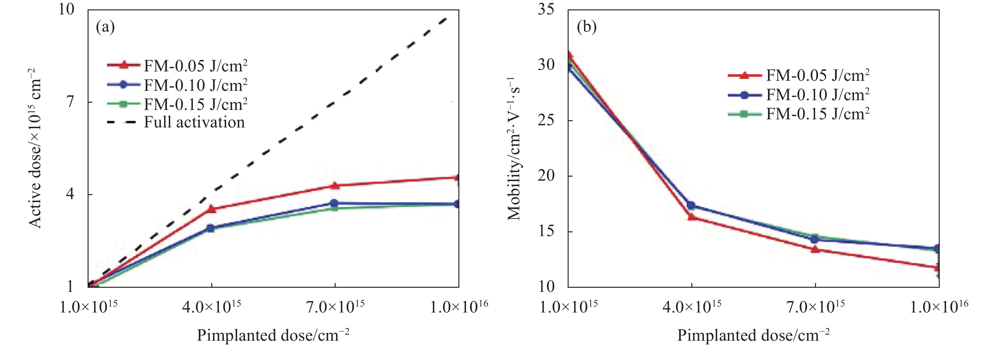
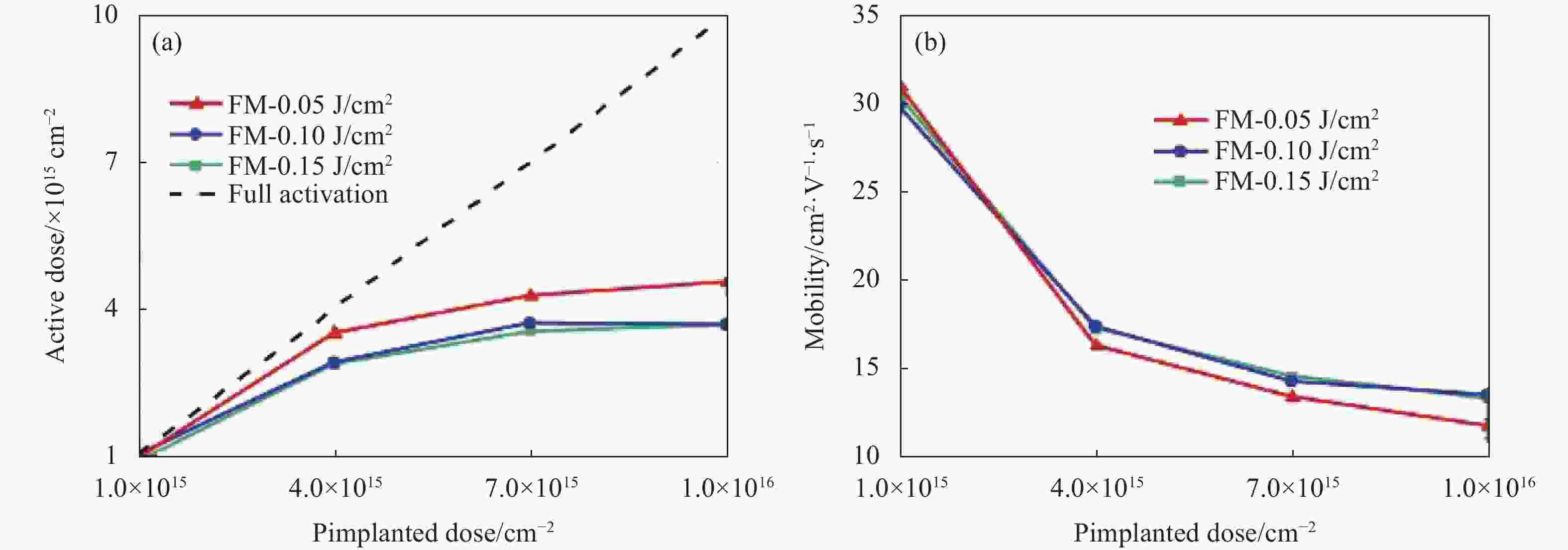
Chery N[72]等使用308 nm的准分子激光对磷注入的SOI器件进行了纳秒准分子激光退火研究。他们研究了通过增加激光能量密度到接近完全熔化阈值对掺杂剂激活影响,激光能量密度的增加对于低剂量注入样品几乎没有影响,其激活率始终接近100%;但是对于高剂量注入的样品,却观察到不同的现象。如图19所示,材料在注入剂量为7×1015 cm−2,激光能量密度为0.15 J/cm2和0.10 J/cm2的退火条件下(未达到完全融化阈值),霍尔剂量(表示被激活掺杂剂量)表现为一个相对恒定的值。相比较而言,在0.05 J/cm2退火条件下,霍尔剂量约4.3×1015 cm−2,增加了约20%,这种霍尔剂量的增加伴随着少量霍尔迁移率(体现载流子的迁移率)的减少。此外,最大激活浓度也随着激光能量密度的增加而增加。这些发现表明,热预算的提升与激光能量密度提升所导致的表面堆积峰值中含磷相关的非活性团簇的溶解有关。
在pMOS中,SiGe与Si相比具有更高的空穴迁移率,10 nm和更高的CMOS制程需要局部的高迁移率Ge和SiGe应变材料[73]。然而由于Si和Ge之间存在晶格不匹配,高浓度的Ge很可能引起SiGe层应变弛豫和位错。为了减少失配位错的成核与扩散,一种通过控制外延生长的方法制备SiGe源/漏的方法被提出。传统的热退火会导致外延生长的高Ge浓度SiGe层产生应变迟豫[74],因此激光退火技术被引入到该制程中,研究人员注意到准分子激光穿透深度浅的特点,使用准分子激光器对外延生长的SiGe沟道材料进行了实验。
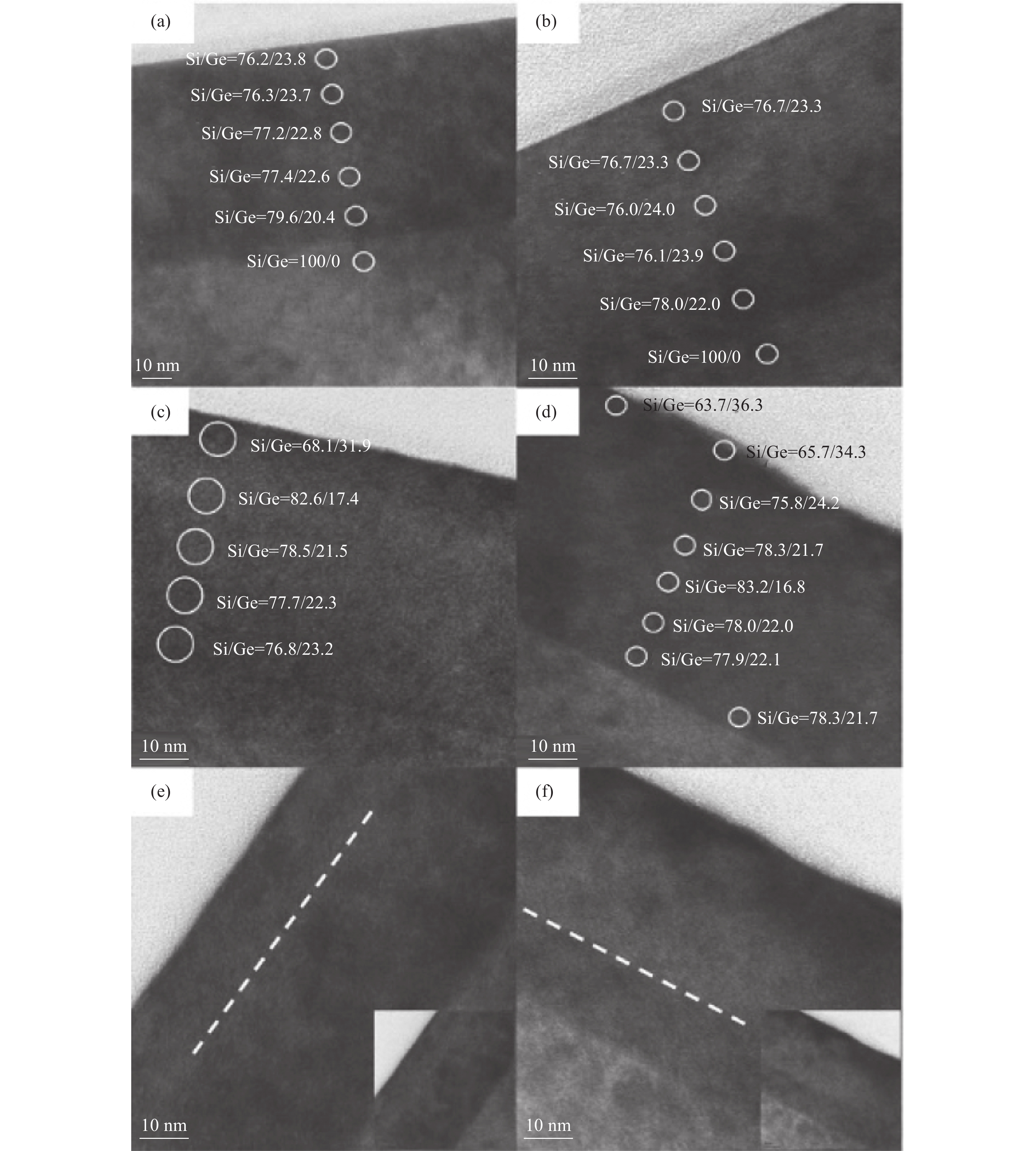
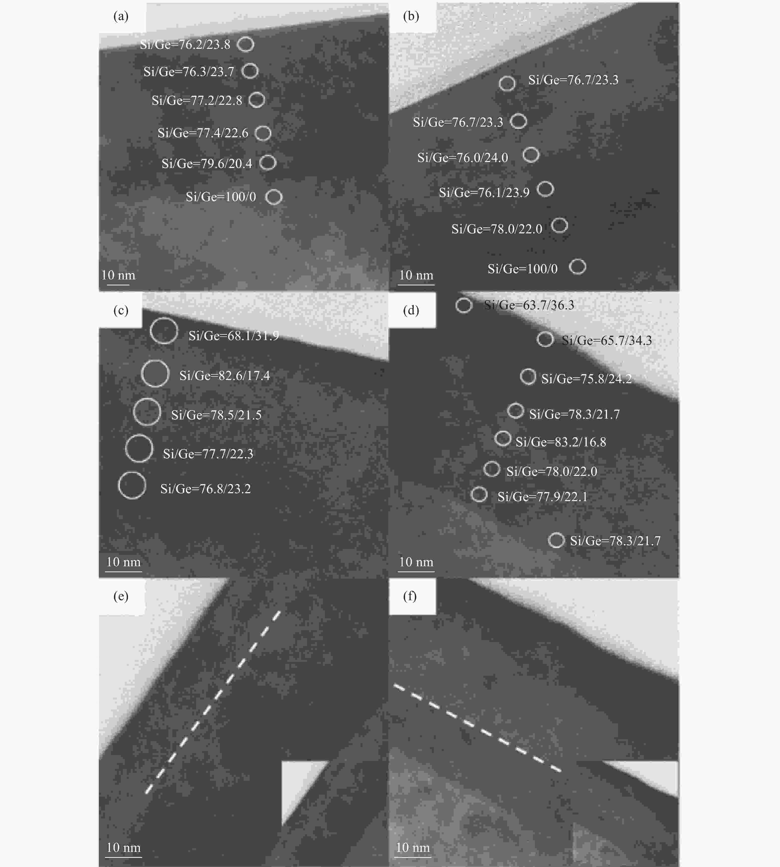
C. Y. Ong[74]等使用不同能量密度的准分子激光对沟道材料进行外延,证明了使用准分子激光可在近表面获得较浅的Si1−yGey梯度层。图20(a)~(d)分别为生长时、0.3 J/cm2、0.5 J/cm2和0.7 J/cm2激光热退火(laser thermal annealing,LTA)后Ge和Si的浓度。经过0.5 J/cm2和0.7 J/cm2准分子激光退火后的样品的透射电子显微镜照片显示,样品中有两个不同的层(图20(e)、(f))。在0.5 J/cm2的LTA条件下,形成了15 nm的Si1-yGey梯度层,表面处Ge浓度最高,为32%。当激光通量增加到0.7 J/cm2时,Si1-yGey梯度层增加到30 nm。
L. Dagault[75]等对Si上的SiGe外延层进行了准分子纳秒激光退火研究,如图21所示,可以看出,在激光退火过程中,表面反射率首先受到温度升高的调制,然后由于固-液相的变化而大幅度增加。固化后,反射率下降到接近初始值。图22为部分熔融状态下样品的显微图以及Ge剖面和面内应变剖面。在1.80 J/cm2时,该层被划分为不同的区域,从Si/SiGe表面约5 nm以下是结晶层,而约5 nm内的近表面区域似乎是非晶态的,且L Dagault还解释道,通过图像的分辨率差异可以观察到熔化层的面内应变曲线显示出比未熔化层更高的变形,表明应力松弛主要发生在熔化部分。然而,即使在未熔化的区域,应变值也没有达到零,这也表明了该层的部分弛豫。


Imen Karmous[76]等使用准分子纳秒激光退火对Si上SiO2/Si堆叠褶皱的产生进行了研究。SiO2/Si堆叠结构对308 nm波长的光的反射率会随者SiO2厚度的变化产生周期性变化,这是由不同界面的反射间的干涉导致的(空气/SiO2和SiO2/Si),使得底层Si的融化能量密度阈值会随着SiO2厚度的变化而变化。此外,对于一定的SiO2厚度,较大的Si熔化深度可能导致Si衬底表面保持熔融的时间增加,进一步使得SiO2薄膜变形或松弛,导致褶皱形成。
-
复杂集成电路中层间互联的质量对集成电路的性能影响很大,因此在新的工艺中引入了更多的金属层,铜曾经就是其中比较典型的材料,但是超过了7 nm节点。新的金属(如:钌)开始作为铜的替代品,因为它在线路电阻和可靠性方面都有潜在的好处。然而相比铜来说,处理钌的热预算要远高于它,高能量的纳秒准分子激光是较为理想的选择。
C. Fenouillet-Beranger[77]等在确定了结激活的退火窗口之后,对脉冲宽度为纳秒级的脉冲激光退火对层间金属互连的影响进行了模拟。他们对器件进行建模,然后在不同的激光能量密度条件下进行激光退火模拟。图23所示为模拟的能量密度0.4 J/cm²、脉冲时间小于200 ns、波长308 nm的准分子激光脉冲温度场和时间演化。模拟结果表明,顶部氧化层厚度对损伤能量密度阈值没有影响,且较大的顶部氧化层厚度有助于降低铜互连的峰值温度。较厚的层间氧化层在激光退火中对底层互连完整性的保留,也使得高能量的纳秒准分子激光在三维集成中的应用前景进一步得到认可。

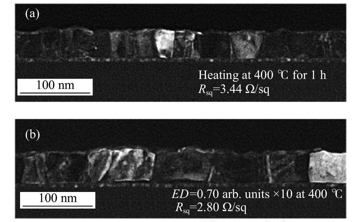
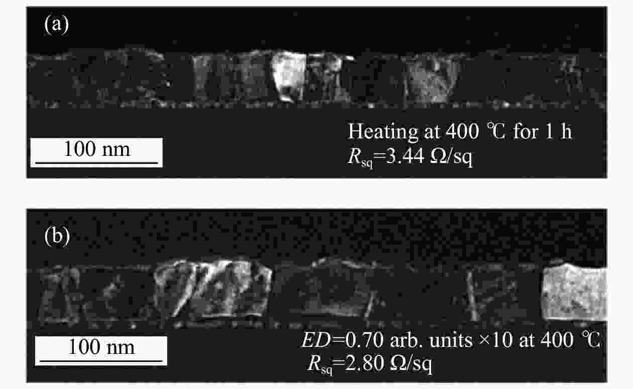
N. Jourdan[78]等研究了纳秒准分子激光退火下,钌薄膜薄层电阻与晶粒生长之间的相关性。图24所示为400 ℃下多次脉冲对薄层电阻的影响,在其设定值的激光照射10次后,逐渐增加激光照射次数,薄膜电阻(sheet resistance,Rsq)会逐渐降低至2.8 Ω/sq。如图25所示,对比400 ℃持续1 h退火和纳秒准分子激光退火的材料截面TEM照片,可以看到纳秒脉冲的准分子激光退火的材料晶粒明显增大,平均晶粒尺寸可以从约23 nm增加到62 nm,N. Jourdan解释道,伴随着晶粒尺寸的变大,薄膜电阻降低了约20%,相较于在纳秒准分子激光退火的情况下,对样品400 ℃持续1 h的退火几乎没有引起薄膜电阻的任何显著变化。
Y. Usami[79]等研究了KrF准分子激光退火对铜和钌半导体器件细金属线的电阻的影响。通过KrF准分子纳秒激光照射后,铜的晶粒尺寸提高了一倍,电阻率降低了20%左右。在钌中,晶粒尺寸增大约1.2倍,电阻率降低约10%,如图26所示。Y. Usami等对实验结果的解释为,激光照射增大金属晶粒尺寸可以抑制电子边界散射,降低电阻率。
-
在3D集成电路中,通过将有源晶体管层层叠加,用介电层隔开,并由金属互连线相互连接,可能是在没有设备缩放的情况下延续摩尔定律的最佳方式。 该方式结构的示意图[80]如图27所示。
但是这种结构在制造时有一些问题,在制造顶层器件时需要较高的热预算,这可能会影响掺杂剂在下层的分布,以及影响顶层以下金属丝的可靠性。晶体管制造中最重要的高热预算过程是高温退火,以激活沟道和源漏区掺杂剂。然而,在这一过程中,下层金属和器件层可能也会被加热,这是不希望产生的,因此脉冲激光退火技术也作为一种有前途的掺杂活化技术被引入。超短、高强度激光脉冲可以使上层器件被融化,而尽可能使下层器件不受影响,在随后的再结晶过程中,上层器件掺杂剂移动到晶格中的取代位点,从而达到激活的目的,为保留下层器件的完整性带来可能。
A. Vandooren[81]等在三维顺序集成(3D sequential integration)的顶层器件中进行了准分子激光源漏的掺杂激活与晶格修复的研究,证明了准分子激光退火可以有效激活外延的硅薄膜器件中n型和p型掺杂,与替代金属栅工艺流程和选择性源/漏外延完全兼容。图28所示为尖峰退火和准分子激光退火器件TEM对比图,图像显示源漏外延层缺陷较小。此外,A. Vandooren等还发现,在经过准分子激光退火后的器件性能至少与经过尖峰退火的器件性能一样好。

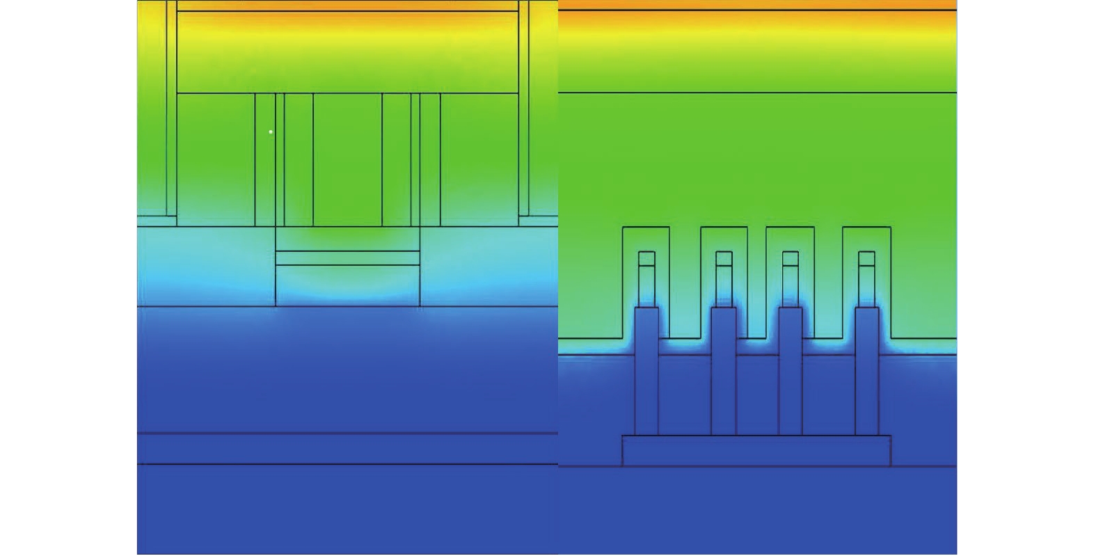
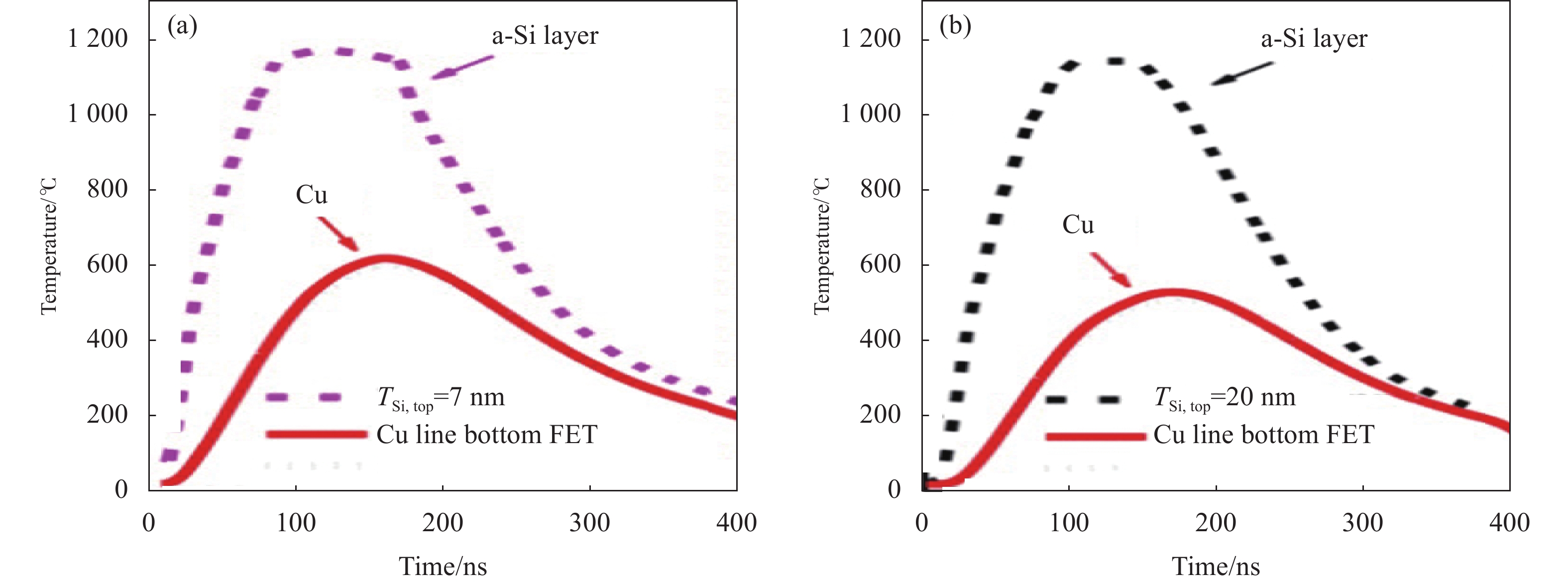
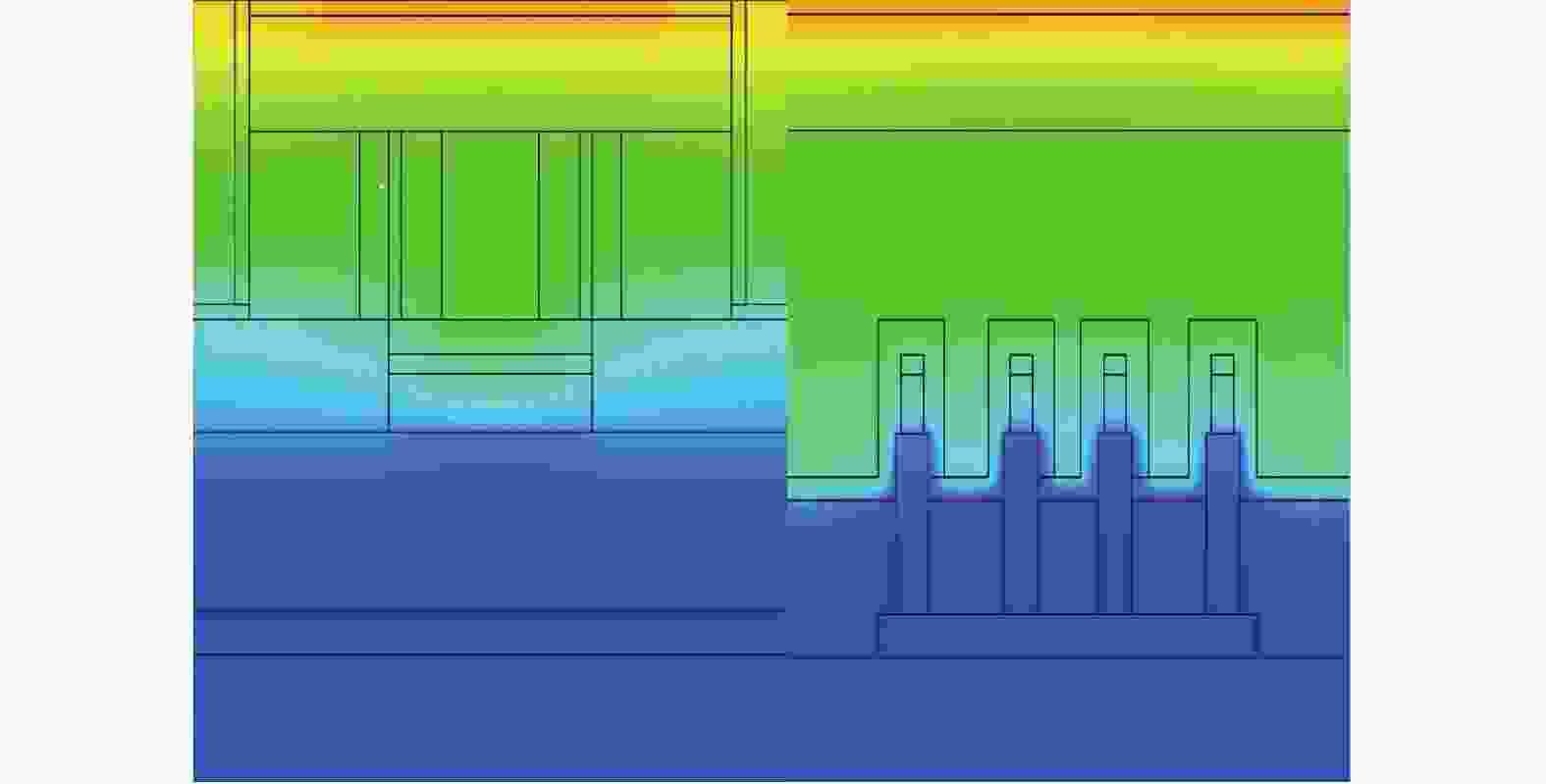
C. Fenouillet-Beranger[82]等首次在先进的原位掺杂源/漏全耗尽SOI技术上量化了底部MOSFET的最大热预算,并且进行了模拟,制作了当时最佳工艺结构模型,提供了瞬时激光电场和二维结构中吸收功率密度的图像,此外还做了一个顶部晶体管上添加一个30 nm的SiN盖层的模型,与没有盖层的情况相比,源漏吸收激光功率的数量和均匀性增加了,如图29所示。

最终通过自制模拟软件(custom simulator)给出了温度场作为时间的函数,得到了模拟器件栅极被激光退火时温度在200 ns内不超过600 ℃的结果,如图30所示。其中模拟使用了波长308 nm、脉冲时间约200 ns的激光。参考文献[82]展示了激光退火在3D堆栈中的前景。
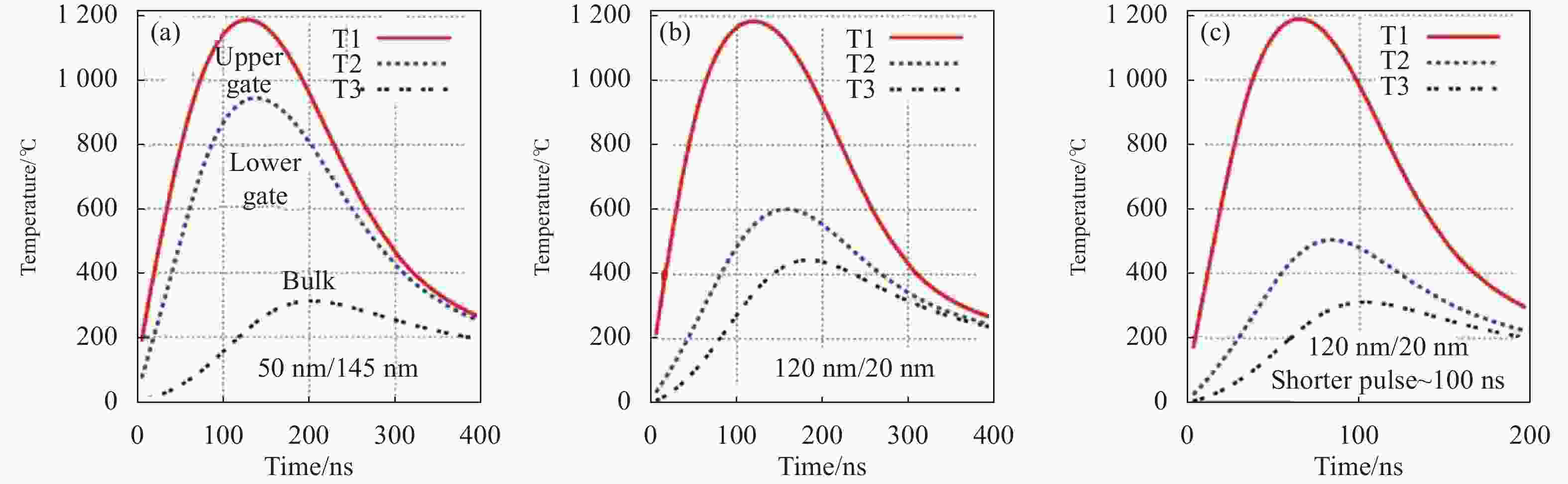
图 30 层间氧化物和底层氧化物的温度与时间的关系。T1: 上层栅极层的温度,T2: 下层栅极层的温度,T3: 体硅顶部的温度[82]
Figure 30. The relationship between temperature and time of interlayer oxides and underlying oxides. T1: the temperature at the upper grid, T2: the temperature at the lower grid, and T3: the temperature at the top of the bulk silicon[82]
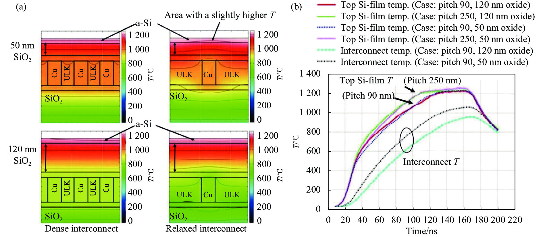
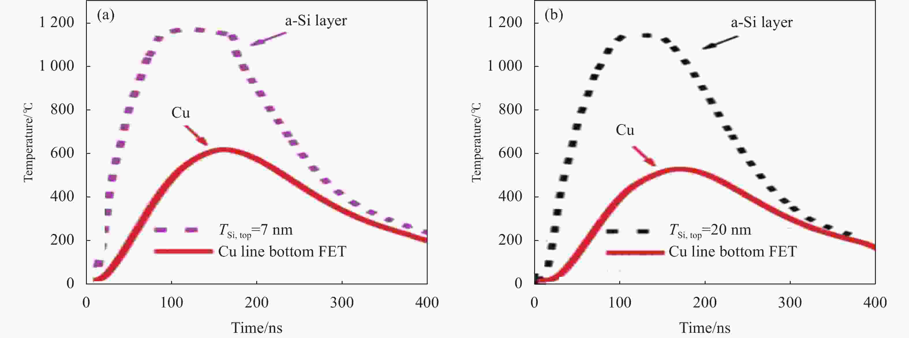
C. Cavalcante[83]等采用160 ns、308 nm的准分子激光对采用FDSOI技术的不同非晶硅厚度28 nm Cu/ULK器件(7 nm和20 nm)进行超快退火的模拟,并且对底层设备和互连结构的抗扰度进行了评估。
在激光退火后,两种非晶硅厚度的器件不管顶部温度如何,即使超过了a-Si的熔体阈值,铜互联线电阻率也保持不变,如图31所示。C. Cavalcante等人还使用LIAB软件进行二维数值模拟,以确定底层所承受的温度。当非晶硅厚度为20 nm时,铜互联线温度仍低于500 ℃,如图32所示;而当非晶硅厚度为7 nm时,铜互联线温度达到600 ℃,但仅为100 ns。证明了使用160 ns、308 nm的准分子激光可以在达到a-Si熔体阈值的条件下不对铜互联线产生影响。

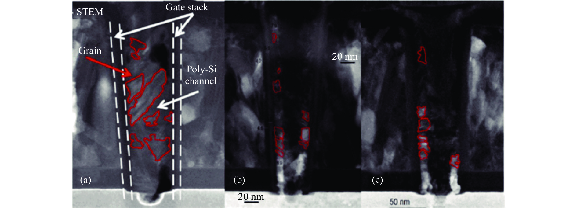
3D垂直沟道器件是新一代NAND非易失性存储器应用的优秀替代方案,其中通心粉结构(macaroni-type)能够提高器件的可控性。在通心粉结构中,完整的多晶硅沟道被薄的多晶硅管所取代,Si的减小可能会转化为较低的串电流,为了提高读取所需的电流,必须对晶界处散射和界面缺陷进行处理。
J. G. Lisoni[84]等对使用准分子激光为全沟道(full channel)器件沟道退火进行了研究,如图33所示。相比快速诱导退火得到的晶粒准分子激光退火LTA得到的晶粒更大,并且在之后的实验中进一步证实,在使用准分子激光退火后不仅会得到更大粒径的晶粒,产生更少缺陷的晶界,还能使得器件的可靠性得到提升。
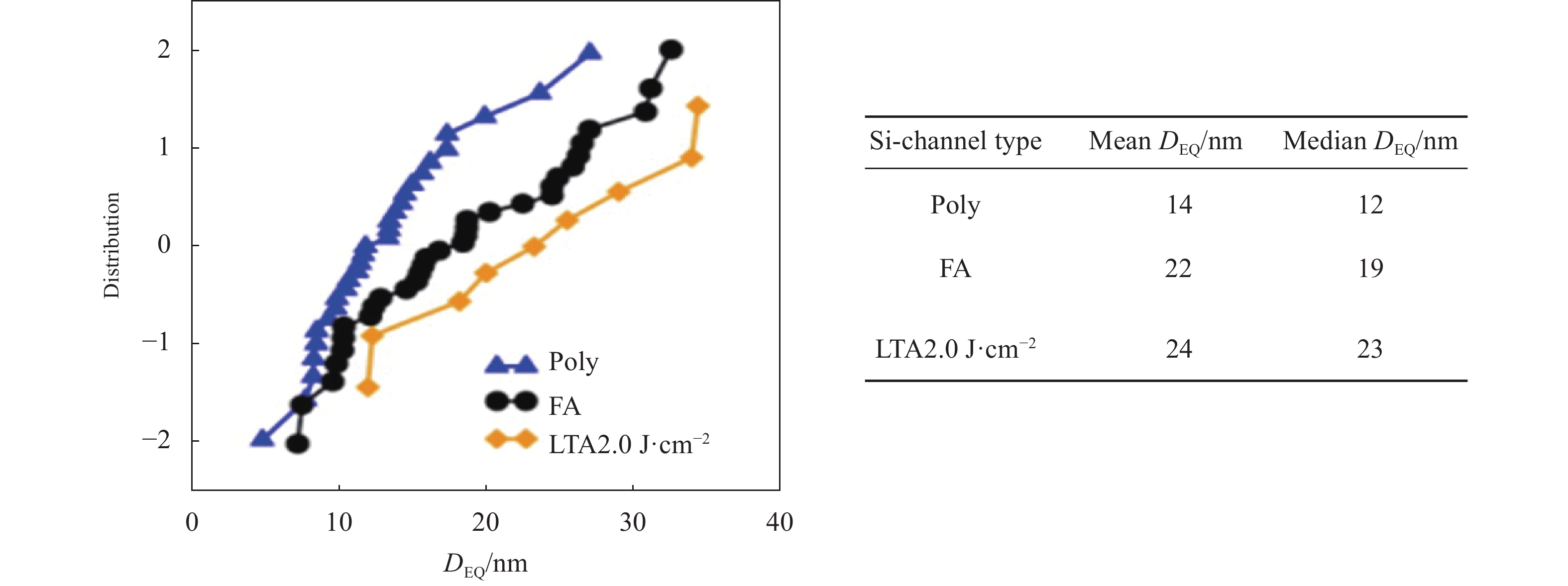
G. Congedo[85]等使用准分子激光对通心粉结构和全沟道结构的沟道退火进行了研究。如图34所示,通心粉结构和全沟道结构中,全沟道器件的晶粒较大,通心粉器件的晶粒较小,而通过激光退火之后对比,未经过激光退火的通心粉器件晶粒结构没有明显改变。图35所示为三种不同情况等效晶粒直径的统计分布,G. Congedo等给出的解释为,在通心粉结构的情况下,较小的可用体积阻止了晶粒向中心扩展,从而限制了等效晶粒直径。
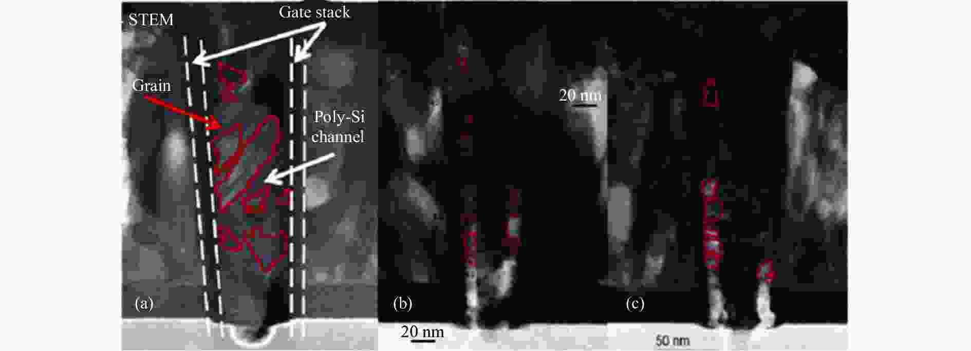
在通心粉结构中,由于可用体积有限且沟道有两个接口,接口缺陷和沟道质量在ID-VG特性中起着极其重要的作用。图36显示,准分子激光退火后的器件缺陷大幅减少,与此同时,器件得到了更高的电流和更低的阈值电压。
-
与传统的退火炉退火以及快速热退火等退火工艺相比,准分子激光器输出激光峰值功率高,波长在紫外区,准分子激光作用于物质表面时能量能迅速地被物质表面吸收,便于对材料表面温度梯度的控制。在半导体集成电路制造的热处理工艺中具有一定优势:准分子激光退火能够有效降低退火热预算并更加精确地控制退火效果,因此,对于准分子激光退火在半导体集成电路制造中的应用已有大量的方法和实验研究结果;准分子激光退火有利于高密度掺杂,获得高的掺杂激活效率,并且能更好地使掺杂原子均匀地分布,控制结深度形成超浅结;准分子激光退火对金属层退火还可以增大金属晶粒尺寸,抑制电子边界散射,降低电阻率,较好的热预算控制也会提高金属的可靠性,为新的工艺中引入高k金属层带来可能;在3D集成电路中,有效减少热预算、提高器件稳定性、解决顶层器件退火对下层掺杂剂分布影响等方面也具备较好的前景。
Research progress of excimer laser annealing in semiconductor integrated circuit manufacturing
-
摘要: 随着半导体集成电路芯片的尺寸越来越小、结构越来越复杂,芯片制造过程中的退火工艺技术也在不断进步。激光退火以其在芯片制造过程中热预算控制的优势,在芯片制造退火工艺中的重要性正在显现。而准分子激光的特点是波长短、峰值功率高、作用于大多数物质表面时能量迅速被物质表面吸收。准分子激光退火可以实现对材料表面温度梯度的控制,是半导体集成电路制造中热处理工艺的重要选择。对半导体集成电路制造过程中准分子激光退火研究进展进行了综述。概述了集成电路制造中退火工艺热预算控制与激光退火的理论模拟研究结果;着重介绍了准分子激光退火在离子掺杂控制、超浅节形成、沟道外延等材料处理中的研究进展,以及在金属层制备和3D器件中的应用。研究表明,准分子激光退火工艺有望为三维半导体集成电路制造提供新的解决方案。Abstract:
Significance In the dynamic landscape of semiconductor device fabrication, continual advancements strive to enhance the process. As the density of transistors per unit area increases and chip components become progressively smaller, the challenges in chip production grow in both intricacy and difficulty. Traditional methods like furnace annealing are becoming inadequate for the evolving demands of chip manufacturing. To address the intricacies posed by shrinking device sizes, annealing techniques and process parameters undergo constant refinement. Pulsed laser annealing emerges as a noteworthy solution, capable of precisely irradiating specific material areas in extremely brief intervals. This technique, harnessed by absorbing laser energy, rapidly elevates the material surface temperature to induce melting. The consequential reconstruction of the melt layer's crystal structure, coupled with redistributed doping in the crystal, serves the crucial purpose of eliminating defect-activated doping. The excimer laser, operating as a nanosecond pulsed ultraviolet laser, holds distinctive attributes that render it particularly meaningful in semiconductor manufacturing annealing technology. Its short wavelength, narrow pulse width, and minimal material penetration depth, especially in semiconductor materials like silicon, contribute to high absorption rates. Moreover, excimer lasers boast high resolution in focusing or projection, coupled with substantial single-pulse energy. This inherent flexibility allows for shaping the energy distribution of the pulse spot, offering adaptability to diverse requirements. These defining characteristics underscore the significance of excimer laser research in advancing semiconductor manufacturing annealing technologies. Progress To optimize the annealing effect in semiconductor manufacturing, it is crucial to shorten the thermal annealing time window and carefully regulate peak temperatures. Controlling the temperature gradient from the material's surface to its interior is a pivotal consideration in annealing technology. Laser annealing is a superior alternative, offering more precise thermal budget control when compared to other methods, as illustrated in Fig.1. Additionally, the perspective of K. Huet et al. on laser thermal budget is presented. Researchers have explored the application of laser annealing in ion doping and epitaxial layer growth. The evolution of doping concentration across different substrates and dopants under excimer laser conditions has been thoroughly investigated. Brief insights into strain silicon technology and silicon on insulator technology are provided, showcasing their integration into semiconductor manufacturing for enhanced device performance. Excimer lasers have been employed by researchers to delve into devices utilizing strained silicon technology and silicon on insulator technology. In the continuous evolution of semiconductor manufacturing processes, there is ongoing innovation in the metal layer. Laser annealing treatment of the metal layer has garnered increased attention, with the reasons for this emphasis briefly explained. Notably, researchers have scrutinized the annealing of metal layers using excimer lasers. The paragraph concludes by briefly addressing the challenges associated with three-dimensional integrated circuit architecture (refer to Fig.27). Manufacturing three-dimensional integrated circuits poses difficulties, particularly in potential damage to the underlying metal and devices during upper-layer annealing. Excimer lasers have emerged as a research focus to address these challenges and optimize the annealing process for three-dimensional integrated circuits. Conclusions and Prospects Excimer laser annealing stands out as a superior choice when compared to alternative annealing methods, particularly evident in the realm of semiconductor integrated circuit manufacturing. The distinct advantages of excimer laser annealing manifest in its exceptional ability to significantly reduce the thermal budget while enabling precise control over the annealing effect. This accuracy proves pivotal in semiconductor manufacturing processes. Moreover, excimer laser annealing brings noteworthy benefits to the table, including the facilitation of high-density doping with enhanced doping activation efficiency. Its unique capacity to distribute doping atoms more effectively and control junction depth contributes to its prominence in the semiconductor industry. The application of excimer laser annealing on metal layers introduces additional advantages. It effectively augments the grain size of the metal, curbing electron boundary scattering, thereby reducing resistivity. This not only enhances the reliability of the metal but also allows for superior thermal budget control. In the context of three-dimensional integrated circuits, excimer laser technology emerges as a transformative solution. It proves highly adept at reducing the thermal budget, a critical consideration in enhancing device stability within these intricate structures. Furthermore, its promising potential lies in addressing the challenges associated with annealing effects on the dopant distribution of the top layer. Excimer laser annealing, with its multifaceted advantages, thus emerges as a promising and versatile solution for optimizing semiconductor manufacturing processes, particularly in the context of three-dimensional integrated circuits. -
Key words:
- semiconductor manufacturing process /
- thermal budget /
- laser annealing /
- excimer laser
-
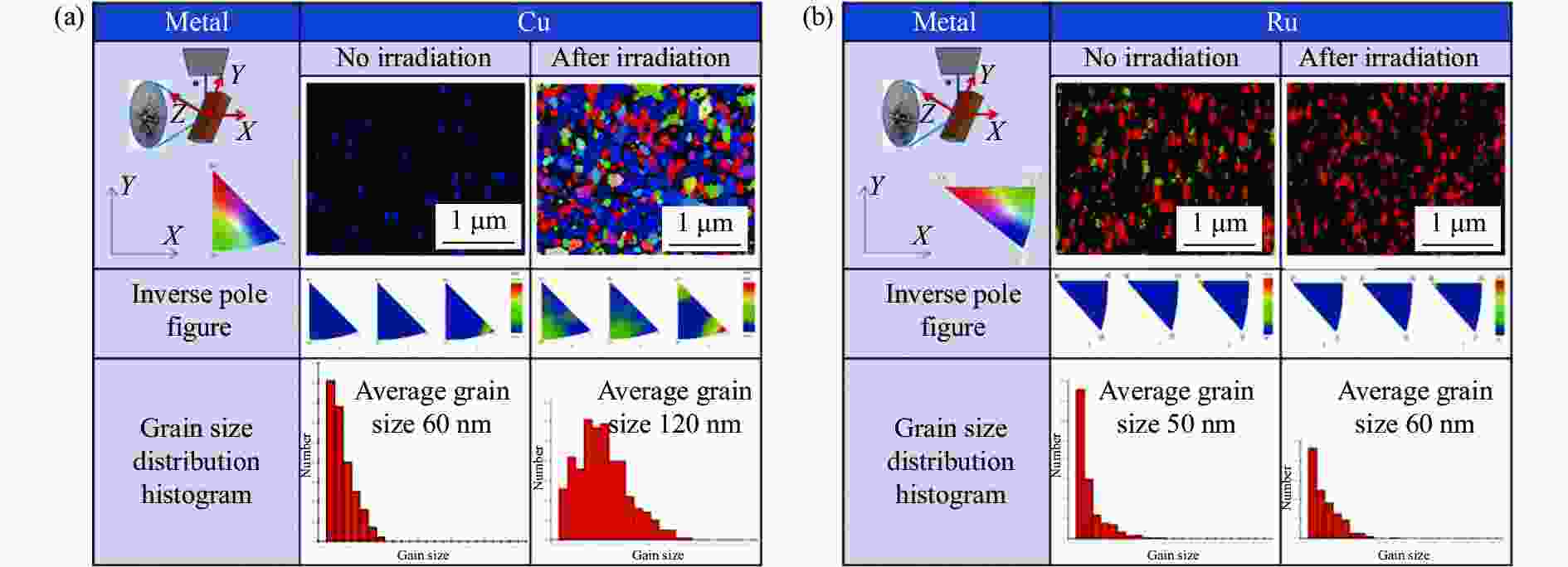
图 30 层间氧化物和底层氧化物的温度与时间的关系。T1: 上层栅极层的温度,T2: 下层栅极层的温度,T3: 体硅顶部的温度[82]
Figure 30. The relationship between temperature and time of interlayer oxides and underlying oxides. T1: the temperature at the upper grid, T2: the temperature at the lower grid, and T3: the temperature at the top of the bulk silicon[82]
-
[1] Razavi Behzad. 模拟CMOS集成电路设计[M]. 陈贵灿, 译. 第2版. 西安: 西安交通大学出版社, 2018: 616-619. [2] Hans-Joachim, Gossmann L, Feng Tao, et al. Reverse diode leakage in spike-annealed ultra-shallowjunctions [J]. MRS Online Proceedings Library (OPL), 2001, 669: J4-J8. doi: https://doi.org/10.1557/PROC-669-J8.4 [3] Felch S, Borland J, Fang Z, et al. Optimized BF3P2 LAD implantation with Si-PAI for shallow, abrupt and high quality p+/n junctions formed using low temperature SPE annealing [C]//Ion Implantation Technology, Proceedings of the 14th International Conference, 2002: 52-55. [4] Borland J O. Low temperature shallow junction formation for 70 nm technology node and beyond [J]. MRS Online Proceedings Library (OPL), 2002, 717: 11. doi: https://doi.org/10.1557/PROC-717-C1.1 [5] Kanemoto Kei, Aharoni Herzl, Ohmi Tadahiro. Ultrashallow and low-leakage p+n junction formation by Plasma Immersion Ion Implantation (PIII) and low-temperature post-implantation annealing [J]. Japanese Journal of Applied Physics, 2001, 40(4): 2706-2711. doi: 10.1143/JJAP.40.2706 [6] Osburn C M, Downey D F, Felch S B, et al. Ultra-shallow junction formation using very low energy B and BF/sub 2/ sources [C]//Proceedings of 11th International Conference on Ion Implantation Technology, 1996: 607-610. [7] Shigeo Onishi, Kenichi Tanaka, Keizo Sakiyama. A new method for evaluating temperature distribution by using Si + + B + implantation [C]//Proceedings of SPIE, 1990, 1189: 83-88. [8] Huet Karim, Mazzamuto Fulvio, Tabata Toshiyuki, et al. Doping of semiconductor devices by laser thermal annealing [J]. Materials Science in Semiconductor Processing, 2017, 62: 92-102. doi: 10.1016/j.mssp.2016.11.008 [9] Murto R, Jones K, Rendon M, et al. Activation and deactivation studies of laser thermal annealed boron, arsenic, phosphorus, and antimony ultra-shallow abrupt junctions [C]//International Conference on Ion Implantation Technology Proceedings. Ion Implantation Technology-2000 (Cat. No. 00EX432), 2000: 155-158. [10] Baeri P, Rimini E. Laser annealing of silicon [J]. Materials Chemistry and Physics, 1996, 46(2): 169-177. [11] Talwar S, Verma G, Weiner K H. Ultra-shallow, abrupt, and highly-activated junctions by low-energy ion implantation and laser annealing[C]//1998 International Conference on Ion Implantation Technology. Proceedings (Cat. No. 98EX144), 1998: 1171-1174. [12] Yu Bin, Wang Yun, Wang Haihong, et al. 70 nm MOSFET with ultra-shallow, abrupt, and super-doped S/D extension implemented by laser thermal process (LTP)[C]//International Electron Devices Meeting 1999. Technical Digest (Cat. No. 99CH36318), 1999: 509-512. [13] Goto K, Yamamoto T, Kubo T, et al. Ultra-low contact resistance for deca-nm MOSFETs by laser annealing [C]//International Electron Devices Meeting 1999. Technical Digest (Cat. No. 99CH36318), 1999: 931-933. [14] Lindfors C D, Jones K S, Law M E, et al. Boron activation during solid phase epitaxial regrowth [J]. MRS Online Proceedings Library (OPL), 2000, 610: B10-B12. [15] Lindsay R, Pawlak B J, Stolk P, et al. Optimisation of junctions formed by solid phase epitaxial regrowth for sub-70 nm CMOS [J]. MRS Online Proceedings Library (OPL), 2002, 717: 21. doi: https://doi.org/10.1557/PROC-717-C2.1 [16] Fung S K H, Huang H T, Cheng S M, et al. 65 nm CMOS high speed, general purpose and low power transistor technology for high volume foundry application [C]//Digest of Technical Papers. 2004 Symposium on VLSI Technology, 2004: 92-93. [17] Hervé Besaucèle, Audrey Adnet, François Beau, et al. High energy excimer laser system for nanosecond annealing of semiconductor devices [C]//Proceedings of SPIE, 2019, 11042: 110420S. [18] Talwar S, Verma G, Weiner K H, et al. Laser thermal processing for shallow junction and silicide formation [C]//Proceedings of SPIE, 1998, 3506: 74-81. [19] Felch S B, Downey D F, Arevalo A, et al. Sub-melt laser annealing followed by low-temperature RTP for minimized diffusion [C]//2000 International Conference on Ion Implantation Technology Proceedings. Ion Implantation Technology-2000 (Cat. No. 00EX432), 2000: 167-170. [20] Talwar S, Markle D, Thompson M O. Junction scaling using lasers for thermal annealing [J]. Solid State Technology 2003, 46(7), 83-84, 86, 88. [21] Pouydebasque A, Dumont B, Denorme S, et al. High density and high speed SRAM bit-cells and ring oscillators due to laser annealing for 45 nm bulk CMOS [C]//IEEE International Electron Devices Meeting, 2005. IEDM Technical Digest, 2005: 663-666. [22] Yamamoto T, Kubo T, Sukegawa T, et al. Junction profile engineering with a novel multiple laser spike annealing scheme for 45-nm node high performance and low leakage CMOS technology [C]//2007 IEEE International Electron Devices Meeting, 2007: 143-146. [23] Triyoso D H, Spencer G, Hegde R I, et al. Laser annealed HfxZr1−xO2 high-k dielectric: Impact on morphology, microstructure, and electrical properties [J]. Applied Physics Letters, 2008, 92(11): 113501. doi: 10.1063/1.2898710 [24] Linder B P, Dasgupta A, Ando T, et al. Process optimizations for NBTI/PBTI for future replacement metal gate technologies [C]//2016 IEEE International Reliability Physics Symposium (IRPS), 2016: 1B-4B. [25] Liu Y, Gluschenkov O, Li J, et al. Strained Si channel MOSFETs with embedded silicon carbon formed by solid phase epitaxy [C]//2007 IEEE Symposium on VLSI Technology, 2007: 44-45. [26] Narasimha S, Chang P, Ortolland C, et al. 22 nm high-performance SOI technology featuring dual-embedded stressors, Epi-Plate High-K deep-trench embedded DRAM and self-aligned via 15LM BEOL [C]//2012 International Electron Devices Meeting, 2012: 3.3.1-3.3.4. [27] Simões S, Calinas R, Vieira M T, et al. In situ TEM study of grain growth in nanocrystalline copper thin films [J]. Nanotechnology, 2010, 21(14): 145701. doi: 10.1088/0957-4484/21/14/145701 [28] Carta F, Gates S M, Limanov A B, et al. Sequential lateral solidification of silicon thin films on Cu BEOL-integrated wafers for monolithic 3-D integration [J]. IEEE Transactions on Electron Devices, 2015, 62(11): 3887-3891. doi: 10.1109/TED.2015.2479087 [29] Liu Z, Gluschenkov O, Niimi H, et al. Dual beam laser annealing for contact resistance reduction and its impact on VLSI integrated circuit variability [C]//2017 Symposium on VLSI Technology, 2017: T212-T213. [30] Liu W H, Luo J W, Li S S, et al. The seeds and homogeneous nucleation of photoinduced nonthermal melting in semiconductors due to self-amplified local dynamic instability [J]. Science Advances, 2022, 8(27): eabn4430. doi: 10.1126/sciadv.abn4430 [31] Sundaram S K, Mazur E. Inducing and probing non-thermal transitions in semiconductors using femtosecond laser pulses [J]. Nature Materials, 2002, 1(4): 217-224. doi: 10.1038/nmat767 [32] Lee C, Srisungsitthisunti P, Park S, et al. Control of current saturation and threshold voltage shift in indium oxide nanowire transistors with femtosecond laser annealing [J]. Acs Nano, 2011, 5(2): 1095-1101. doi: 10.1021/nn102723w [33] Smith M J, Lin Y T, Sher M J, et al. Pressure-induced phase transformations during femtosecond-laser doping of silicon [J]. Journal of Applied Physics, 2011, 110(5): 053524. [34] Chen C, Chen G, Yang H, et al. Solution-processed metal oxide arrays using femtosecond laser ablation and annealing for thin-film transistors [J]. Journal of Materials Chemistry C, 2017, 5(36): 9273-9280. doi: 10.1039/C7TC01953J [35] Frank M M, Cartier E A, Lavoie C, et al. Crystallization of hafnium-oxide-based ferroelectrics for BEOL integration [C]//2022 6th IEEE Electron Devices Technology & Manufacturing Conference (EDTM). IEEE, 2022: 316-318. [36] Bayer L, Ye X, Lorenz P, et al. Studies on perovskite film ablation and scribing with ns-, ps-and fs-laser pulses [J]. Applied Physics A, 2017, 123: 1-8. doi: 10.1007/s00339-016-0611-9 [37] 刘敏, 郑柳, 何志等. 硅晶圆中注入10 MeV磷的连续激光退火激活[J]. 激光与红外, 2022, 52(07): 1000-1003. doi: 10.3969/j.issn.1001-5078.2022.07.008 Liu Min, Zheng Liu, He Zhi, et al. Continuous laser annealing for activating 10 MeV implanted phosphorus in silicon wafer [J]. Laser & Infrared, 2022, 52(7): 1000-1003. (in Chinese) doi: 10.3969/j.issn.1001-5078.2022.07.008 [38] 王怡哲, 喻学昊, 刘墨林等. 低抖动准分子激光放大器光源的研究[J]. 红外与激光工程, 2023, 52(03): 170-176. Wang Yizhe, Yu Xuehao, Liu Molin, et al. Study on light source of low jitter excimer laser amplifier [J]. Infrared and Laser Engineering, 2023, 52(3): 20220468. (in Chinese) [39] Scott J C, Gluschenkov O, Goplen B, et al. Reduction of RTA-driven intra-die variation via model-based layout optimization [C]//2009 Symposium on VLSI Technology, 2009: 152-153. [40] Miyashita T, Kubo T, Kim Y S, et al. A study on millisecond annealing (MSA) induced layout dependence for flash lamp annealing (FLA) and laser spike annealing (LSA) in multiple MSA scheme with 45 nm high-performance technology [C]//2009 IEEE International Electron Devices Meeting (IEDM), 2009: 1-4. [41] Huet Karim, Tabata Toshiyuki, Aubin Joris, et al. Laser thermal annealing for low thermal budget applications: from contact formation to material modification (invited) [J]. ECS Transactions, 2019, 89(3): 137. doi: 10.1149/08903.0137ecst [42] Lombardo S F, Fisicaro G, Deretzis I, et al. Theoretical study of the laser annealing process in FinFET structures [J]. Applied Surface Science, 2019, 467-468: 666-672. doi: 10.1016/j.apsusc.2018.10.155 [43] Dagault L, Kerdilès S, Acosta A P, et al. Investigation of recrystallization and stress relaxation in nanosecond laser annealed Si1−xGex/Si epilayers [J]. Applied Surface Science, 2020, 527: 146752. doi: 10.1016/j.apsusc.2020.146752 [44] Ni C N, Rao K V, Khaja F, et al. Ultra-low NMOS contact resistivity using a novel plasma-based DSS implant and laser anneal for post 7 nm nodes [C]//2016 IEEE Symposium on VLSI Technology, 2016: 1-2. [45] Tabata T, Aubin J, Huet K, et al. Super activation of highly surface segregated dopants in high Ge content SiGe obtained by melt UV laser annealing [C]//22nd International Conference on Ion Implantation Technology (IIT), 2018: 353-356. [46] Tabata T, Aubin J, Huet K, et al. Impact of solidification velocity on activation of Ga, In, and Al segregated in high Ge content SiGe by UV melt laser anneal [C]//2019 Electron Devices Technology and Manufacturing Conference (EDTM), 2019: 130-132. [47] Tabata Toshiyuki, Aubin Joris, Huet Karim, et al. Segregation and activation of Ga in high Ge content SiGe by UV melt laser anneal [J]. Journal of Applied Physics, 2019, 125(21): 215702. doi: 10.1063/1.5096889 [48] Everaert J L, Schaekers M, Yu H, et al. Sub-10−9 Ω·cm2 contact resistivity on p-SiGe achieved by Ga doping and nanosecond laser activation [C]//2017 Symposium on VLSI Technology, 2017: T214-T215. [49] Yu H, Wang L L, Schaekers M, et al. Lanthanum and lanthanum silicide contacts on N-type silicon [J]. IEEE Electron Device Letters, 2017, 38(7): 843-846. doi: 10.1109/LED.2017.2700233 [50] Yu H, Schaekers M, Schram T, et al. Multiring circular transmission line model for ultralow contact resistivity extraction [J]. IEEE Electron Device Letters, 2015, 36(6): 600-602. doi: 10.1109/LED.2015.2425792 [51] Li C I, Breil N, Wen T Y, et al. p-type MOSFET contact resistance improvement by conformal plasma doping and nanosecond laser annealing [J]. IEEE Electron Device Letters, 2019, 40(2): 307-309. doi: 10.1109/LED.2019.2890950 [52] van Dal M J H, Vellianitis G, Doornbos G, et al. Ge CMOS gate stack and contact development for Vertically Stacked Lateral Nanowire FETs[C]//2018 IEEE International Electron Devices Meeting (IEDM), 2018: 21.1.1-21.1.4. [53] Wang Z, Mingo N. Diameter dependence of SiGe nanowire thermal conductivity [J]. Applied Physics Letters, 2010, 97(10): 101903. doi: 10.1063/1.3486171 [54] Mingo Natalio, Yang Liu, Li Deyu, et al. Predicting the thermal conductivity of Si and Ge nanowires [J]. Nano Letters, 2003, 3(12): 1713-1716. doi: 10.1021/nl034721i [55] Hung R, Khaja F A, Hollar K E, et al. Novel solutions to enable contact resistivity <1E-9 Ω-cm2 for 5 nm node and beyond [C]//2018 International Symposium on VLSI Technology, Systems and Application (VLSI-TSA), 2018: 1-2. [56] Lee R T P, Petrov N, Kassim J, et al. Nanosecond laser anneal for BEOL performance boost in advanced FinFETs[C]//2018 IEEE Symposium on VLSI Technology, 2018: 61-62. [57] Batude P, Fenouillet-Beranger C, Pasini L, et al. 3 DVLSI with CoolCube process: An alternative path to scaling [C]//2015 Symposium on VLSI Technology (VLSI Technology), 2015: T48-T49. [58] Fenouillet-Beranger C, Batude P, Brunet L, et al. Recent advances in 3D VLSI integration [C]//2016 International Conference on IC Design and Technology (ICICDT), 2016: 1-4. [59] Bosch D, Alba P A, Kerdiles S, et al. Laser processing for 3D junctionless transistor fabrication [C]//2019 IEEE SOI-3D-Subthreshold Microelectronics Technology Unified Conference (S3S), 2019: 1-3. [60] Derakhshandeh J, Tajari Mofrad M R, Ishihara R, et al. A study of the CMP effect on the quality of thin silicon films crystallized by using the μ-Czochralski process [J]. Journal of the Korean Physical Society, 2009(54): 432-436. [61] Ishihara R, van der Wilt P C, van Dijk B D, et al. Location-control of large grains by μ-czochralski (grain filter) process and its application to single-crystalline silicon thin-film transistors [J]. Thin Solid Films, 2003, 427(1-2): 77-85. [62] Lisoni J G, Arreghini A, Congedo G, et al. Laser thermal anneal of polysilicon channel to boost 3D memory performance [C]//2014 Symposium on VLSI Technology (VLSI-Technology): Digest of Technical Papers, 2014: 1-2. [63] Huet K, Boniface C, Negru R, et al. Ultra low thermal budget anneals for 3D memories: Access device formation [J]. AIP Conference Proceedings, 2012, 1496(1): 135-138. [64] Congedo G, Arreghini A, Liu L, et al. Analysis of performance/variability trade-off in Macaroni-type 3-D NAND memory [C]//2014 IEEE 6th International Memory Workshop (IMW), 2014: 1-4. [65] La Magna Antonino, Alippi Paola, Privitera Vittorio, et al. A phase-field approach to the simulation of the excimer laser annealing process in Si [J]. Journal of Applied Physics, 2004, 95(9): 4806-4814. doi: 10.1063/1.1690861 [66] Fortunato G, Mariucci L, Stanizzi M, et al. Ultra-shallow junction formation by excimer laser annealing and low energy (<1 keV) B implantation: A two-dimensional analysis [J]. Nuclear Instruments and Methods in Physics Research Section B: Beam Interactions with Materials and Atoms, 2002, 186(1): 401-408. [67] Chong Y F, Pey K L, Wee A T S, et al. Annealing of ultrashallow p+/n junction by 248 nm excimer laser and rapid thermal processing with different preamorphization depths [J]. Applied Physics Letters, 2000, 76(22): 3197-3199. doi: 10.1063/1.126627 [68] Do Seungloo, Kong Seong, Lee Yonglyun, et al. Ultra-shallow junction formation using plasma doping and excimer laser annealing for nano-technology CMOS applications [J]. Journal of the Korean Physical Society, 2009, 55: 1065-1069. doi: 10.3938/jkps.55.1065 [69] Aid S R, Rashid N N M, Jonny N F A, et al. Preliminary study on laser annealed NP Junction in phosphorus implanted germanium [C]//2020 IEEE International Conference on Semiconductor Electronics (ICSE). IEEE, 2020: 152-155. [70] Tabata T, Raynal P E, Huet K, et al. Segregation and activation of Sb implanted in Si by UV nanosecond-laser-anneal-induced non-equilibrium solidification[J]. Journal of Applied Physics, 2020, 127(13): 135701. [71] Kim Seong-Dong, Park Cheol-Min, Woo J C S. Advanced source/drain engineering for box-shaped ultrashallow junction formation using laser annealing and pre-amorphization implantation in sub-100-nm SOI CMOS [J]. IEEE Transactions on Electron Devices, 2002, 49(10): 1748-1754. doi: 10.1109/TED.2002.803634 [72] Chery N, Zhang M, Monflier R, et al. Study of recrystallization and activation processes in thin and highly doped silicon-on-insulator layers by nanosecond laser thermal annealing [J]. Journal of Applied Physics, 2022, 131(6): 65301. doi: 10.1063/5.0073827 [73] Borland J, Qin S, Oesterlin P, et al. High mobility Ge-channel formation by localized/selective liquid phase epitaxy (LPE) using Ge+B plasma ion implantation and laser melt annealing [C]//2013 13th International Workshop on Junction Technology (IWJT), 2013: 49-53. [74] Ong C Y, Pey K L, Li X, et al. Laser annealing induced high Ge concentration epitaxial SiGe layer in Si1−xGex virtual substrate [J]. Applied Physics Letters, 2008, 93(4): 41112. doi: 10.1063/1.2962991 [75] Dagault L, Acosta-Alba P, Kerdiles S, et al. Impact of UV nanosecond laser annealing on composition and strain of undoped Si0.8Ge0.2 epitaxial layers [J]. ECS Journal of Solid State Science and Technology, 2019, 8: 202-208. doi: 10.1149/2.0191903jss [76] Karmous I, Rozé F, Raynal P E, et al. Non-equilibrium growth of surface wrinkles emerging in an SiO2/Si stack during Si melting induced by UV nanosecond pulsed laser annealing [J]. ECS Journal of Solid State Science and Technology, 2022, 11(10): 104006. doi: 10.1149/2162-8777/ac9beb [77] Fenouillet-Beranger C, Acosta-Alba P, Mathieu B, et al. Ns laser annealing for junction activation preserving inter-tier interconnections stability within a 3D sequential integration [C]//2016 IEEE SOI-3D-Subthreshold Microelectronics Technology Unified Conference (S3S), 2016: 1-2. [78] Jourdan N, Roze F, Tabata T, et al. UV nanosecond laser annealing for Ru interconnects [C]//2020 IEEE International Interconnect Technology Conference (IITC), 2020: 163-165. [79] Usami Y, Imokawa K, Nohdomi R, et al. Change in resistivity of fine metal line by KrF excimer laser annealing [C]//2022 IEEE International Interconnect Technology Conference (IITC), 2022: 108-110. [80] Rajendran B, Jain S H, Kramer T A, et al. Thermal simulation of laser annealing for 3D integration [C]//Proceedings VMIC, 2003: 1-6. [81] Vandooren A, Wu Z, Parihar N, et al. 3D sequential low temperature top tier devices using dopant activation with excimer laser anneal and strained silicon as performance boosters [C]//2020 IEEE Symposium on VLSI Technology, 2020: 1-2. [82] Fenouillet-Beranger C, Mathieu B, Previtali B, et al. New insights on bottom layer thermal stability and laser annealing promises for high performance 3D VLSI [C]//2014 IEEE International Electron Devices Meeting, 2014: 25-27. [83] Cavalcante C, Fenouillet-Beranger C, Batude P, et al. 28 nm FDSOI CMOS technology (FEOL and BEOL) thermal stability for 3D sequential integration: yield and reliability analysis [C]//2020 IEEE Symposium on VLSI Technology, 2020: 1-2. [84] Lisoni J G, Arreghini A, Congedo G, et al. Laser thermal annealneal of polysilicon channel to boost 3D memory performance [C]//2014 Symposium on VLSI Technology (VLSI-Technology): Digest of Technical Papers, 2014: 1-2. [85] Congedo G, Arreghini A, Liu L, et al. Analysis of perfor-mance/variability trade-off in Macaroni-type 3-D NAND memory [C]//2014 IEEE 6th International Memory Workshop (IMW), 2014: 1-4. -

 点击查看大图

图(36)
计量
- 文章访问数: 152
- HTML全文浏览量: 59
- PDF下载量: 46
- 被引次数: 0

