


 下载:
下载:


-
随着科技发展,头戴显示器开始变得越来越轻、越来越小,逐渐形成了眼镜式或者护目式的近眼显示系统(Near-Eye-Display,NED)[1]。其中增强现实(Augmented Reality,AR)是一种将虚拟信息与真实世界相融合进行显示的技术,广泛运用于多媒体、智能交互、传感等多种技术手段,将计算机生成的虚拟物体、场景或系统提示信息叠加到真实场景中,从而实现对现实场景的“增强”。早在20世纪50年代,AR就已经应用在国防领域,而随着2021年“元宇宙”概念的提出,近眼显示设备被认为是元宇宙的媒介而成为研究热点[2]。近年来,人们对AR显示的需求也在不断提升,对高分辨、高亮度的微型显示设备和小体积、轻质量的近眼显示光学系统需求越来越迫切 [3-6]。
光学引擎模组是AR近眼显示设备的核心组件,其性能是直接影响成像质量和制造成本的关键因素。从技术发展现状来看,AR 近眼显示技术多采用双目视差立体透视显示模式,通过不同类型光学模组的设计方案将真实场景与虚拟图像融合显示。传统近眼显示存在视场和体积不能兼顾的技术问题,具有亚波长尺寸的超表面则为AR光学引擎的光调控提供了一条新的可行思路。
光学超表面是一种由亚波长周期结构排列而成的人工材料,可任意改变光的电磁波传播,具有传统材料无法实现的特殊性质。采用相位不连续的方式调控光波的波前, 可实现光波的异常反射与异常折射,以及光场偏振等的任意调控[7-11]。
应用超表面于AR近眼显示光学系统的部分代表性工作。2018年,Byoungho Lee团队[12]通过二色镜等元件改变不同波长的成像位置来实现消色差,将直径 20 mm、数值孔径为 0.61 的超表面用于搭建AR 系统原理样机,实现了90°的单色视场和76°的全色成像视场,共极化传输效率在红、绿、蓝的光谱中达到 79%。2021年,Couplers. T. Afra.[13]团队设计并模拟了单眼光波导显示器,在右梯形波导上用结晶硅椭圆超表面阵列作为耦合器,实现了80°水平大视场(FOV)这比基于衍射光栅的传统波导系统中的FOV高大约80%。2022年,Chee Wei Wong[14]团队通过对超表面每个单元的精心设计,设备实现了1080PPI分辨率,视野超过40°,总输入输出效率超过1%。同时,相关文献指出,通过单个超表面波导层来实现AR波导,有助于扩展性和工艺成品率的控制。美国罗切斯特大学Daniel[15] 等人采用自由曲面型衬底,通过超表面与自由曲面协同调控光场的方式,实现了AR功能。这种由超表面和自由曲面组成的结构被称为超曲面。
利用超表面进行光相位调控,主要可总结为三种方法:分别为共振相位调控、传输相位调控[16]和几何相位调控[17]。共振相位调控是通过改变共振频率来实现相位突变,共振频率由纳米级结构的几何形状控制;传输相位是由于电磁波在传播的过程中会产生光程差,利用这一特性可实现对相位的调控;几何相位是一种通过调整具有相同尺寸微纳结构的旋转角度,实现光波的相位突变。其中,基于传输相位原理设计的超表面,通常由各向同性的微纳米结构构成,具有高度对称的特点[18-23]。由此设计的超表面对入射光偏振不敏感,即微纳米结构的相位响应与入射光的偏振类型无关,且易于获得较高的效率,非常适合于光波导型AR光学引擎。
由于传输相位型超表面对偏振光不敏感且具有很高的传输效率,在光波导结构中有很大的应用潜力,因此文中在AR近眼显示光学引擎的光波导结构中引入传输相位超表面作为光耦出结构。通过改变单元结构的半径和周期可调节光束的偏转角度,设计结果充分证明了该设计的有效性。
-
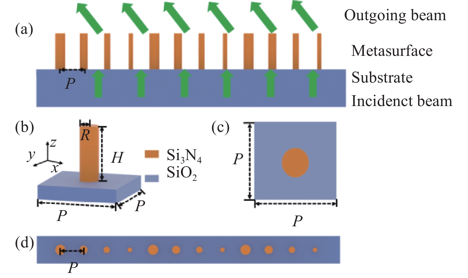
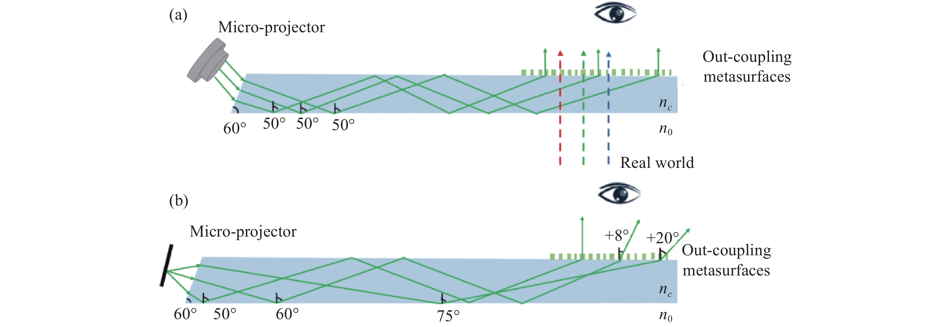
文中采用超表面耦出结构的AR近眼显示光波导结构示意图如图1 所示,图1(a)为入射光在波导全反射角为50°时出射光准直耦出示意图,图1(b) 为20°视场角的出射光示意图,其中采用Micro-LED显示芯片作为近眼显示系统的Micro-projector像源,Micro-LED具有亮度高、高发光效率、低能耗、高反应速度、高对比度与色彩饱和度,被认为是新一代理想显示技术[24-28]。图1中大面积蓝色部分为光波导结构,波导内填充材料为二氧化硅(SiO2)(折射率nc =1. 46),其全反射临界角为43.23°,当入射光在波导内传播角度大于43.23°时可实现全反射(n0 = 1) ,其耦入部分采用切角为60°的波导,通过改变入射光角度,使入射光在波导内传播全反射角度在50°~75°。在光耦出区域设计了超表面结构,该超表面由衬底和周期性纳米柱组成,其衬底材料为SiO2,衬底和波导为同一材料,纳米柱材料为氮化硅(Si3N4),Si3N4折射率虚部为0,是无损介质,即在超表面材料中使用氮化硅可以实现更高的传输效率,且具有较高的热稳定性和化学稳定性,可以在高温环境下工作而不会发生严重的性能退化,工作的时间更长而损耗小。其共振特性会引起相位变化,使得结构表面形成相位分布的周期性梯度变化,并使入射光发生偏转。

图 1 采用超表面耦出结构的AR光波导结构示意图。(a) 准直出射;(b) 20°视场角出射
Figure 1. Structure diagram of AR optical waveguide with hypersurface coupling structure. (a) Collimated emission; (b) 20° field of view angle exit
-
传统的光学元件根据光在传播过程中逐步累积相位差,实现了对光束进行偏转或聚焦,这一过程相位是渐变的,不存在相位突变。而超表面通过人为设计的纳米尺度结构单元,使该界面具有传统界面所不具备的特性,当光波经过该界面时,实现对光波或电磁波的任意调制。超表面单元结构可以在二维平面形成突变相位,可以用费马原理解释突变相位的产生,即当光波在介质中进行传播时,所经过的光路的光程是相等的[29]。对于由两种介质构成的光学界面,平面波从A点以入射角θi入射,并经过界面上B点,若平面波沿界面方向的相位不连续,则A、B两点之间存在两条无限接近的光传播路径,它们之间的相位差为零,即:
$$ \begin{gathered} \left[ {{k_0}{n_i}\sin {\theta _i}{\rm{d}}x + (\phi + {\rm{d}}\phi )} \right] - ({k_0}{n_t}\sin {\theta _t}{\rm{d}}x + \phi ) = 0 \\ \end{gathered} $$ (1) 式中:θt为折射角;ϕ和ϕ+dϕ为两条路径中的光分别穿过界面时的相位;
dx 为两条路径在界面处的距离;ni和nt分别为两个介质的折射率;k0=2π/λ0,λ0为波长。整理公式(1)可得: $$ {n}_{t}\mathrm{sin}{\theta }_{t}-{n}_{i}\mathrm{sin}{\theta }_{i}=\frac{{\lambda }_{0}}{2\pi }\cdot \frac{{\rm{d}}\phi }{{\rm{d}}x} $$ (2) 在入射角不变的情况下,改变界面的相位梯度dϕ/dx,则折射角θt随之改变,符合广义折射定律(图2)。

图 2 广义折射率推导示意图
Figure 2. Schematic diagram of derivation of generalized refractive index
传输相位型超表面主要为基于介质材料的单层周期结构,可以用等效折射率理论解释,即通过改变亚波长纳米柱的占空比来改变等效折射率,从而实现相位调控光波经过微结构所产生的相位累积,可以用下式近似表示为:
$$ \Delta \phi = 2\pi {n_{eff}}\frac{{{\lambda _0}}}{h} $$ (3) 式中:neff、h、λ0分别为微结构的等效折射率、微结构的高度和工作波长。通常情况下,为了方便工艺的制备,微结构的高度是固定的,通过改变微结构的有效折射率来实现在特定波长和特定高度条件下的波前控制。利用时域有限差分算法可得到垂直入射时光束透过超表面结构所产生的相位延迟,该相位延迟使得界面的相位呈现梯度变化,从而改变光的透射方向,据此可设计透射式超表面结构以实现垂直入射时的光束偏转。
-
由于超表面的光学特性主要是由亚波长结构决定的,因此,通过优化亚波长结构的一系列几何参数(形状、材料、角度等) ,获得需要的光学响应(振幅、相位、偏振态等) ,就能设计相应功能的超表面。
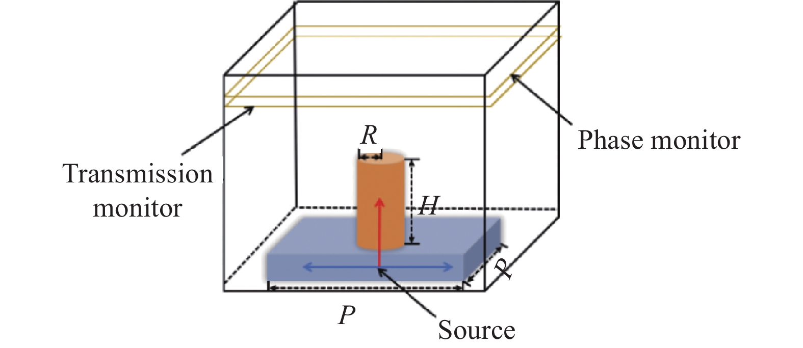
文中是基于时域有限差分法FDTD进行计算,设纳米柱高度和半径分别为H和R,周期为P。改变半径和高度都会改变相位延迟,这里考虑到加工制备,将高度固定只改变半径。在周期一定时变化高度和半径,寻找相位分布和透射率最佳的高度尺寸。单元结构仿真模型如图3所示,光源为平面波向上入射,入射光波长设置为550 nm,入射角度和偏振角度均为0。仿真范围为黑色框内区域,仿真区域边界条件设为完美吸收层。采用xy 面监视器作为透射率监视器,采用点监视器作为相位监视器[30]。

图 3 单元结构仿真模型
Figure 3. Simulation model of unit structure
确定P和H之后,确保在半径R变化时,电场相位能够覆盖0~2π相位区间,且相位变化速度应均匀。利用仿真确定相位变化范围和透射率分布,仿真验证部分结果如图4所示。扫描参数为:周期P=250 nm,高度H为800~1200 nm,半径R为50~120 nm。为提高加工容错度,使不同基元之间尺寸变化较大,选择相位变化较慢的高度。Si3N4在550 nm时折射率为2.05,实部相比于常用的介质材料更低,光程差小,在相位变化扫描时,相位随半径变化缓慢,相位的一个周期为2π,达到2π时超表面对光波的调节能力较强,因此需要增加高度来满足相位达到2π。考虑到加工方面,深宽比应尽量小,所以选择900 nm 作为纳米柱高度、最小直径为100 nm,即最大深宽比为9∶1。

图 4 相位和透射率扫描结果。(a)透射率随半径变化图;(b)相位随半径变化图;(c) 透射率随半径和高度变化图; (d)相位随半径和高度变化图
Figure 4. Phase and transmittance scanning results. (a) Diagram of transmittance variation with radius; (b) Diagram of phase variation with radius; (c) Diagram of transmittance variation with radius and height; (d) Diagram of phase variation with radius and height
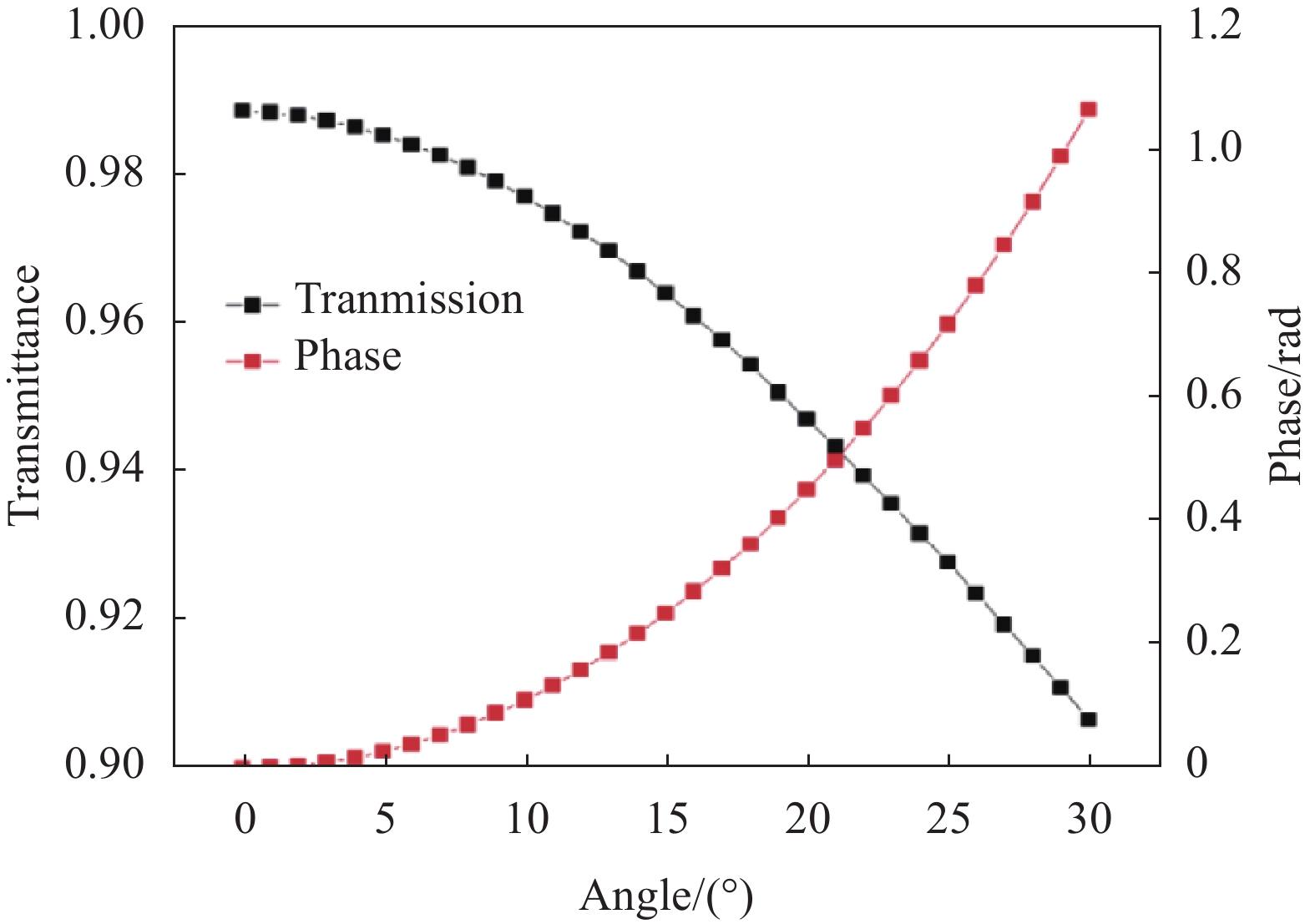
超表面单元结构可以表现出随入射光角度变化的响应特性,因此,同一个超表面结构对不同角度的入射光表现出特定的相响应,即可实现对不同角度入射光的不同波前调控。当高度为900 nm,半径为80 nm时,改变入射光角度,相位和透射率会发生变化。图5为在0°~30°时不同角度的相位和透射率的变化。其透射率和相位移随着入射角度的增加而不规则地变化,对于斜入射光,纳米柱会激发共振效应,导致其透射率降低。

图 5 透射率和相位随角度变化图
Figure 5. Change of transmittance and phase with angle
所设AR光波导耦出超表面的角度偏转示意图如图6(a)所示,这里超表面单元间的相位延迟呈梯度排列,每四个纳米柱为一个周期,结构俯视图如图6(d)所示。超表面由排列在正方形周期单元上的介质柱组成,图6(b) 和6(c) 分别为单元结构的俯视图和侧视图。

图 6 (a) 超表面角度偏转示意图;(b)~(c) 具有高度H、半径为R的超表面单元结构的侧视图和俯视图,周期为P;(d)构建的角度偏转超表面的俯视图
Figure 6. (a) Metasurface angle deflection diagram; (b)-(c) Side view and top view of the metasurface cell structure with height H and radius R, the unit cell size is P; (d) Top view of the constructed angular deflection metasurface
-
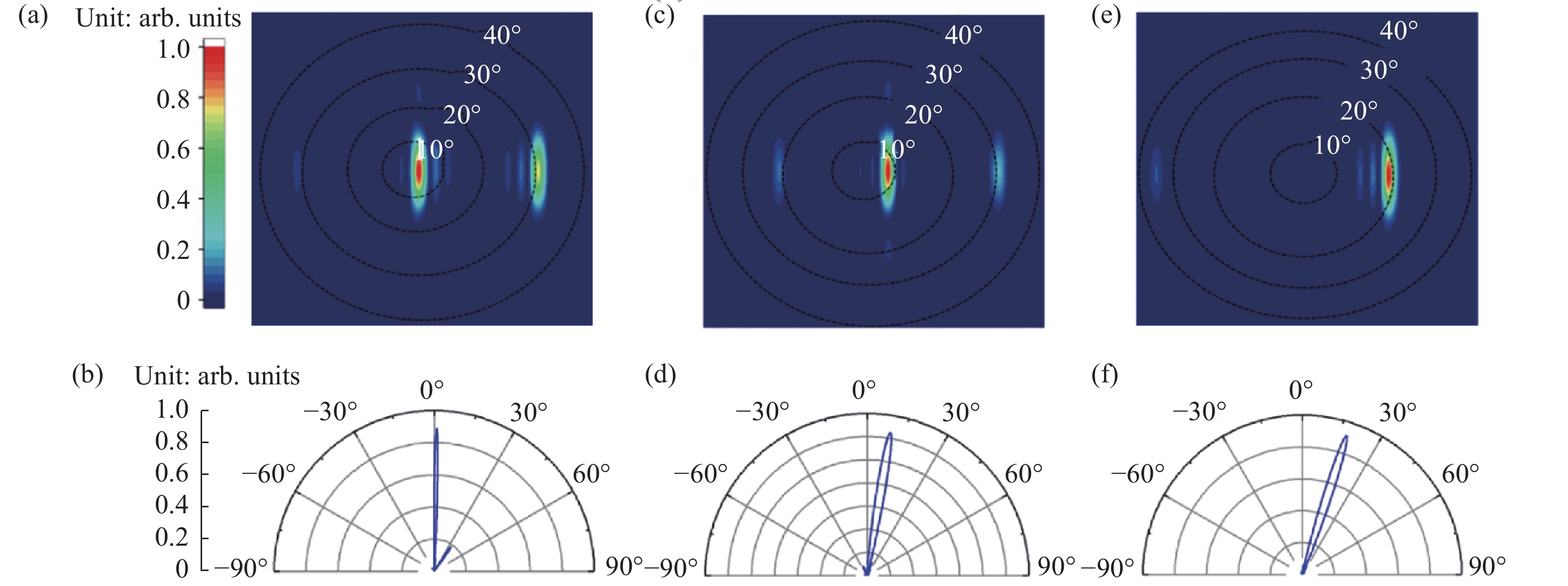
当入射光准直入射时,仿真出射光偏离z轴−35°(顺时针为+,逆时针为−)。通过放置监视器或远场计算等方式观察场强分布,通过计算得到偏转效率达77%,偏转效率定义为所设计角度内的能量比总的入射光能量。准直入射时出射光场强分布和角度分布如图7所示。从场强分布图和角度分布图中可以看出,出射光的大部分能量都集中在−35°,符合设计要求,但是在0°附近也有少部分能量漏出,其原因是超表面结构前一个周期的最后一个纳米柱和后一个周期的第一个纳米柱之间没有相位差,因此在入射光经过时不会发生偏转。
图8为超表面在设计波长±30 nm范围内的出射光角度分布。文中所设计超表面的工作波长是参照文献报道的InGaN/AlGaN纳米线绿光Micro-LED[31],其发射光谱如图8(a)所示,当电流为350 mA时,主波长为550 nm,半高宽为60 nm。图8(b)展示了所设计超表面在不同波长范围内出射光的角度分布,并由此分析偏转角与入射波长的对应关系,取出图中不同入射波长曲线中偏转角度的横坐标,得到图8(c)。可以看出器件的偏转角度在所设计角度5°范围内波动,是因为此结构是针对波长为550 nm进行相位扫描,当波长变化时相位差也会发生变化,所以对不同波长的光束会出现不同的波前调控。

图 7 准直入射时出射光场强分布和角度分布图。(a) 光场强分布图;(b) 角度分布图
Figure 7. The field intensity distribution and angle distribution of the outgoing light at collimation incident. (a) Distribution of optical field intensity; (b) Angular distribution map

图 8 超表面在设计波长±30 nm 范围内的出射光角度分布。(a)绿色Micro-LED的电致发光特性图[31];(b) 出射光在不同角度的透射率分布;(c) 偏转角度与入射波长的关系图
Figure 8. Dispersion characteristics of the metasurface in the range of ±30 nm. (a) Electroluminescence characteristics of green Micro-LED[31]; (b) Transmission distribution of the outgoing light at different angles; (c) The relation between deflection angle and incident wavelength
-
在FDTD简化模拟了AR近眼显示光波导,将光源放在波导内侧模拟全反射入射光,通过改变入射角进行耦出角的变化模拟。由于同一个超表面结构对不同角度的入射光表现出特定的相位响应,即可实现对不同角度入射光的不同波前调控。当入射角为+50°时光场在耦出端经超表面耦出,耦出角为0°,随着入射角度的增加耦出角度也逐渐增大;当入射角为+60°时光场在耦出端经超表面耦出,耦出角为偏离z轴+8°;当入射角为+75°时光场在耦出端经超表面耦出,耦出角为偏离z轴+20°。因此,该系统可实现20°的视场角。耦出角为0°、+8°、+20°场强分布和角度分布如图9所示。

图 9 出射光角度偏转光强和角度分布图。(a)、(b)为耦出角0°的场强分布和角度分布图;(c)、(d)为耦出角+8°的场强分布和角度分布图;(e)、(f)为耦出角+20°的场强分布和角度分布图
Figure 9. Distribution of light intensity and angle of deflection. (a) and (b) are the field intensity distribution and angle distribution diagrams decoupled at angle 0°; (c) and (d) are the field intensity distribution and angle distribution diagram of decoupled angle +8°; (e) and (f) are the field intensity distribution and angle distribution diagram of decoupled angle +20°
进一步分析了AR光学引擎光场分布在波导、超表面结构和空气中z轴方向上的动态变化过程。图10(a)~(c)分别为入射角+50°时光场在波导、超表面结构中和空气的分布图;图图10(d)~(f)分别为入射角+60°时光场在波导、超表面结构和空气的分布图;图图10(g)~(i)分别为入射角+75°时光场在波导、超表面结构中和空气的分布图。从图中可以明显看到,当入射光在波导内传播时,由于光的传播介质为各向同性的均匀介质,没有突变相位的引入,因此入射光在波导内的传播方向不会改变;当光经过超表面时,由于超表面单元引入了突变相位,且相邻单元结构引入的突变相位之差为∆Φ,等相位面因而产生偏转;在完全经过超表面后由于超表面引入的相位差,光的传播方向由50°~75°偏转至0°~20°。
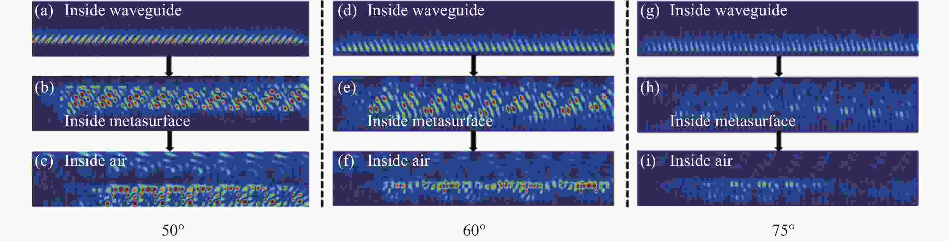
图 10 (a)~(c)分别为入射角50°时光场在波导、超表面结构中和耦出超表面的分布图;(d)~(f)分别为入射角60°时光场在波导、超表面结构中和耦出超表面的分布图;(g)~(i)分别为入射角75°时光场在波导、超表面结构中和耦出超表面的分布图
Figure 10. (a)-(c) are the distribution of the time field in the waveguide, the metasurface structure and the coupled metasurface at the incidence angle of 50°, respectively; (d)-(f) are the distribution of the time field in the waveguide, the metasurface structure and the coupled metasurface at the incidence angle of 60°, respectively; (g)-(i) respectively represent the distribution of the time field in the waveguide and the metasurface structure and the coupled metasurface at the incident angle of 75°
-
文中设计了一种适用于AR近眼显示光波导的超表面耦出结构,利用超表面结构由共振特性引发的相位周期性的梯度变化,通过改变结构半径和高度实现出射光角度偏转,对不同角度入射光产生不同波前调控。结果表明,光在小角度入射时的偏转效率可高达77%,通过改变入射光在波导内的全反射角度,耦出角随着入射角的变化而改变,最终可实现了20°视场角。超表面的引入为AR近眼显示光学引擎设计提供了有效方案,对实现质量轻、结构紧凑眼镜形态AR模组有重要意义,有望成为AR 近眼显示光学引擎的潜在发展方向。
Design of waveguide decoupled metasurface for augmented reality display optical engine (invited)
-
摘要: 增强现实(AR)近眼显示光学引擎是新型显示光学设计领域的研究热点之一,它将虚拟图像投射到现实物理环境中进行显示,在空间上增强、融合和补充了物理世界。AR 近眼显示光学引擎在光学系统集成化和微型化方面有较高要求,眼镜形态的AR近眼显示光学设备是未来必然发展趋势。光学超表面是一种由亚波长单元结构在二维平面上周期排布而成的人工结构阵列,通过单元结构和电磁波的相互作用实现对光场中振幅、相位和偏振的任意调控,同时具有体积小、效率高、结构紧凑等特点,在近眼显示应用中具有很大潜力。文中在AR光学引擎设计中引入一种传输相位型超表面光波导耦出结构,该超表面单元引入了突变相位,通过对超表面的等相位面调控改变光经过波导耦出的角度,使出射光效率最高达到77%,并实现20°视场角,为AR光波导结构设计提供一种可行方案,有望为下一代人机交互显示平台提供解决方案。Abstract:
Object The optical engine design of augmented reality (AR) near-eye display is one of the research hotspots in the field of display technology. It projects virtual images to the real physical environment for display, and simultaneously enhances, merges, and complements the physical world in space. AR near-eye display optical engine has high requirements for the integration and miniaturization of optical system, and the glass-like AR near-eye display optical device is an inevitable development trend in the future. Optical metasurface is an artificial structure array composed of subwavelength unit structure periodically arranged on a two-dimensional plane. It realizes arbitrary regulation of the amplitude, phase, and polarization of the light field through the interaction of the unit structure and electromagnetic wave. At the same time, it has the characteristics of small size, high efficiency, and compact structure, and has great potential in near-eye display applications. Methods In this paper, a metasurface structure is designed as the decoupled structure of the AR near-eye display optical waveguide (Fig.1). The decoupled part adopts a waveguide with a cutting angle of 60°. By changing the angle of incident light, the incident light propagates inside the waveguide at 50°-75°. The coupled part of the metasurface has a height of 900 nm and a radius of 50-120 nm (Fig.6). The AR near-eye display optical waveguide is simplified and simulated in FDTD. The light source is placed inside the waveguide to simulate the total reflection of the incident light, and the decoupling angle is simulated by changing the incident angle. Results and Discussions When the collimated light is incident into the metasurface structure, the outgoing light deviates from the z-axis by −35° (Fig.7). The field intensity distribution is observed by placing a monitor or far-field calculation, and the deflection efficiency is calculated to reach 77%. In addition, the angle distribution of the outgoing light on the metasurface within the designed wavelength of ±30 nm is simulated, and it can be seen that the deflection angle of the device fluctuates within the designed angle of 5° (Fig.8). Since the same metasurface structure has a specific phase response to incident light at different angles, different wavefront adjustment of incident light at different angles can be realized. Waveguide with a cutting angle of 60° is adopted in the coupled part. By changing the incident light angle, the incident light can propagate in the waveguide at 50°-75°, and the variation range of the outgoing optical coupling angle is 0°-20°. There is a one-to-one correspondence between the angle change of the incident light and the angle change of the outgoing light (Fig.9). Conclusions A metasurface coupling structure for AR near-eye display optical waveguide is designed. The metasurface structure can be deflected by changing the radius and height of the structure, and the wavefront of the incident light at different angles is controlled. The results show that the deflection efficiency of light at a small incident angle can be as high as 77%. By changing the total reflection angle of the incident light in the waveguide, the coupling angle changes with the change of the incident angle, and finally the field of view angle of 20° can be achieved. The introduction of metasurface provides an effective scheme for the design of AR near-eye display optical engine, which is of great significance for the realization of light-weight and compact eyeglass for a AR module, and is expected to become a potential development direction of AR near-eye display optical engine. -
Key words:
- near-eye display /
- optical waveguide /
- metasurface /
- transmission phase /
- augmented reality /
- beam deflection
-
图 1 采用超表面耦出结构的AR光波导结构示意图。(a) 准直出射;(b) 20°视场角出射
Figure 1. Structure diagram of AR optical waveguide with hypersurface coupling structure. (a) Collimated emission; (b) 20° field of view angle exit
图 2 广义折射率推导示意图
Figure 2. Schematic diagram of derivation of generalized refractive index
图 4 相位和透射率扫描结果。(a)透射率随半径变化图;(b)相位随半径变化图;(c) 透射率随半径和高度变化图; (d)相位随半径和高度变化图
Figure 4. Phase and transmittance scanning results. (a) Diagram of transmittance variation with radius; (b) Diagram of phase variation with radius; (c) Diagram of transmittance variation with radius and height; (d) Diagram of phase variation with radius and height
图 6 (a) 超表面角度偏转示意图;(b)~(c) 具有高度H、半径为R的超表面单元结构的侧视图和俯视图,周期为P;(d)构建的角度偏转超表面的俯视图
Figure 6. (a) Metasurface angle deflection diagram; (b)-(c) Side view and top view of the metasurface cell structure with height H and radius R, the unit cell size is P; (d) Top view of the constructed angular deflection metasurface
图 7 准直入射时出射光场强分布和角度分布图。(a) 光场强分布图;(b) 角度分布图
Figure 7. The field intensity distribution and angle distribution of the outgoing light at collimation incident. (a) Distribution of optical field intensity; (b) Angular distribution map
图 8 超表面在设计波长±30 nm 范围内的出射光角度分布。(a)绿色Micro-LED的电致发光特性图[31];(b) 出射光在不同角度的透射率分布;(c) 偏转角度与入射波长的关系图
Figure 8. Dispersion characteristics of the metasurface in the range of ±30 nm. (a) Electroluminescence characteristics of green Micro-LED[31]; (b) Transmission distribution of the outgoing light at different angles; (c) The relation between deflection angle and incident wavelength
图 9 出射光角度偏转光强和角度分布图。(a)、(b)为耦出角0°的场强分布和角度分布图;(c)、(d)为耦出角+8°的场强分布和角度分布图;(e)、(f)为耦出角+20°的场强分布和角度分布图
Figure 9. Distribution of light intensity and angle of deflection. (a) and (b) are the field intensity distribution and angle distribution diagrams decoupled at angle 0°; (c) and (d) are the field intensity distribution and angle distribution diagram of decoupled angle +8°; (e) and (f) are the field intensity distribution and angle distribution diagram of decoupled angle +20°
图 10 (a)~(c)分别为入射角50°时光场在波导、超表面结构中和耦出超表面的分布图;(d)~(f)分别为入射角60°时光场在波导、超表面结构中和耦出超表面的分布图;(g)~(i)分别为入射角75°时光场在波导、超表面结构中和耦出超表面的分布图
Figure 10. (a)-(c) are the distribution of the time field in the waveguide, the metasurface structure and the coupled metasurface at the incidence angle of 50°, respectively; (d)-(f) are the distribution of the time field in the waveguide, the metasurface structure and the coupled metasurface at the incidence angle of 60°, respectively; (g)-(i) respectively represent the distribution of the time field in the waveguide and the metasurface structure and the coupled metasurface at the incident angle of 75°
-
[1] Zhu Encheng, Han Jian, Zhong Ziquan, et al. Augmented reality near-eye display and its military applications[C]//Chinese Institute of Command and Control. Proceedings of the 5th China Command and Control Conference, 2017: 228-233. (in Chinese) [2] Zhou Ziping, Li Yao, Yan Yinguo, et al. Current situation and trend ofMicro-LED application in near-eye display [J]. Chinese Journal of Liquid Crystals and Displays, 2022, 37(6): 661-679. [3] Li Y, Jiang H, Yan Y, et al. Highly efficient and ultra-compact micro-LED pico-projector based on a microlens array [J]. Journal of the Society for Information Display, 2023, 31: 483-493. doi: 10.1002/jsid.1215 [4] Jiang H, Lin Z, Li Y, et al. Design of self-luminous pico-projection optical engine based on a quantum-dot color converted micro-LED[C]//SPIE, 2022, 12448: 303-309. [5] 李洋洋, 张超, 杨宁, 等. 超表面在增强现实近眼显示中的应用研究进展[J]. 激光与光电子学进展, 2022, 59(20): 69-81. Li Yangyang, Zhang Chao, Yang Ning, et al. Research progress on application of metasurface concept in augmented reality near-Eye displays [J]. Laser & Optoelectronics Progress, 2022, 59(20): 69-81. (in Chinese) [6] 罗栩豪, 董思禹, 王占山, 等. 超表面 VR/AR 显示技术研究进展[J]. 激光与光电子学进展 , 2022, 59(20): 30-46. Luo Xuhao, Dong Siyu, Wang Zhanshan, et al. Research progress of metasureface-based VR/AR display technology [J]. Laser & Optoelectronics Progress, 2022, 59(20): 30-46. (in Chinese) [7] Yu N, Genevet P, Kats M A, et al. Light propagation with phase discontinuities: generalized laws of reflection and refraction [J]. Science, 2011, 334(6054): 333-337. doi: 10.1126/science.1210713 [8] Khorasaninejad M, Chen W T, Devlin R C, et al. Metalenses at visible wavelengths: Diffraction-limited focusing and subwavelength resolution imaging [J]. Science, 2016, 352(6290): 1190-1194. doi: 10.1126/science.aaf6644 [9] Yu N F, Capasso F. Flat optics with designer metasurfaces [J]. Nature Materials, 2014, 13: 139-150. doi: 10.1038/nmat3839 [10] Zhan A, Dodson C M, Majumdar A. Metasurface freeform nanophotonics [J]. Science Reports, 2017, 7: 1673. doi: 10.1038/s41598-017-01908-9 [11] 廖琨, 甘天奕, 胡小永, 等. 基于介质超表面的片上集成纳米光子器件[J]. 光学学报, 2021, 41(8): 0823001. Liao Kun, Gan Tianyi, Hu Xiaoyong, et al. On-chip nanophotonic devices based on dielectric metasurfaces [J]. Acta Optica Sinica, 2021, 41(8): 0823001. (in Chinese) [12] Lee G Y, Hong J Y, Hwang S, et al. Metasurface eyepiece for augmented reality [J]. Nature Communications, 2018, 9(1): 4562. [13] Afra T, Salehi M R, Abiri E. Design of two compact waveguide display systems utilizing metasurface gratings as couplers [J]. Applied Optics, 2021, 60(28): 8756-8765. doi: 10.1364/AO.428733 [14] Boo H, Lee Y S, Yang H, et al. Metasurface wavefront control for high-performance user-natural augmented reality waveguide glasses [J]. Scientific Reports, 2022, 12(1): 5832. doi: 10.1038/s41598-022-09680-1 [15] Nikolov D K, Bauer A, Cheng F, et al. Metaform optics: Bridging nanophotonics and freeform optics [J]. Science Advances, 2021, 7(18): 5112. [16] Liu Z, Feng W, Long Y, et al. A metasurface beam combiner based on the control of angular response [J]. Photonics, 2021, 8(11): 0489. [17] Chen W T, Zhu A Y, Sanjeev V, et al. A broadband achromatic metalens for focusing and imaging in the visible [J]. Nature Nanotechnology, 2018, 13(3): 220-226. doi: 10.1038/s41565-017-0034-6 [18] Huang J, Hu Z, Gao X, et al. Unidirectional-emitting GaN-based micro-LED for 3D display [J]. Optics Letters, 2021, 46(14): 3476-3479. doi: 10.1364/OL.430021 [19] Khaidarov E, Liu Z, Paniagua-domínguez R, et al. Control of LED emission with functional dielectric metasurfaces [J]. Laser & Photonics Reviews, 2020, 14(1): 1900235. [20] 蒲欣欣, 周顺, 肖相国, 等. 近红外偏振无关超透镜研究[J]. 应用光学, 2020, 41(03): 591-596. Pu Xinxin, Zhou Shun, Xiao Xiangguo, et al. Research on near-infrared polarization-independent metalens [J]. Journal of Applied Optics, 2020, 41(3): 591-596. (in Chinese) [21] 陈磊, 严金华, 郭焕祥, 等. 基于硅基超表面的高效率大角度光束偏转[J]. Acta Optica Sinica, 2021, 41(3): 0305001. Chen Lei, Yan Jinhua, Guo Huanxiang, et al. Highly efficient large-angle beam deflection based on silicon-based metasurface [J]. Acta Optica Sinica, 2021, 41(3): 0305001. (in Chinese) [22] 王艺霖, 范庆斌, 徐挺. 电磁超表面透镜的前沿成像应用进展[J]. 红外与激光工程, 2021, 50(05): 95-106. Wang Yilin, Fan Qingbin, Xu Ting. Progress of advanced imaging applications based on electromagnetic metalens [J]. Infrared and Laser Engineering, 2021, 50(5): 20211026. (in Chinese) [23] 莫昊燃, 纪子韬, 郑义栋, 等. 超表面透镜的宽带消色差成像(特邀)[J]. 红外与激光工程, 2021, 50(01): 40-49. Mo Haoran, Ji Zitao, Zheng Yidong, et al. Broadband achromatic imaging with metalens (Invited) [J]. Infrared and Laser Engineering, 2021, 50(1): 20211005. (in Chinese) [24] 胡新培, 蔡俊虎, 叶媛媛, 等. 高光效GaN基Micro-LED仿真模型研究[J]. 光学学报, 2022, 42(15): 204-213. Hu Xinpei, Cai Junhu, Ye Yuanyuan, et al. Simulation model of GaN-based Micro-LED with high light extraction efficiency [J]. Acta Optica Sinica, 2022, 42(15): 1525001. (in Chinese) [25] Hu X, Cai J, Liu Y, et al. Design of inclined omni-directional reflector for sidewall-emission-free micro-scale light-emitting diodes [J]. Optics & Laser Technology, 2022, 154: 108335. [26] Chen E, Zhao M, Chen K, et al. Metamaterials for light extraction and shaping of micro-scale light-emitting diodes: from the perspective of one-dimensional and two-dimensional photonic crystals [J]. Optics Express, 2023, 31(11): 18210-18226. doi: 10.1364/OE.489598 [27] Zhang X, Chen A, Yang T, et al. Tripling light conversion efficiency of μLED displays by light recycling black matrix [J]. IEEE Photonics Journal, 2022, 14(2): 1-7. [28] Liu Y, Xia T, Du A, et al. Omnidirectional color shift suppression of full-color micro-LED displays with enhanced light extraction efficiency [J]. Optics Letters, 2023, 48(7): 1650-1653. doi: 10.1364/OL.486014 [29] 仇宫润, 赵峰, 王琨. 近红外超透镜的设计与制备[J]. 应用光学, 2021, 42(6): 1102. Qiu Gongrun, Zhao Feng, Wang Kun. Design and fabrication of near-infrared metalens [J]. Journal of Applied Optics, 2021, 42(6): 1102-1106. (in Chinese) [30] 徐碧洁, 陈向宁, 赵峰, 等. 近红外波长超透镜的设计与仿真[J]. 激光与红外, 2021, 51(11): 1466-1471. Xu Bijie, Chen Xiangning, Zhao Feng, et al. Near infrared wavelength metalens design and simulation [J]. Laser & Infrared, 2021, 51(11): 1466-1471. (in Chinese) [31] Bui H Q T, Velpula R T, Jain B, et al. Full-color InGaN/AlGaN nanowire micro light-emitting diodes grown by molecular beam epitaxy: A promising candidate for next generation micro displays [J]. Micromachines, 2019, 10(8): 492. doi: 10.3390/mi10080492 -

 点击查看大图
计量
- 文章访问数: 342
- HTML全文浏览量: 50
- PDF下载量: 120
- 被引次数: 0

