


-
基于回音壁模式的微盘激光器具有非常高的品质因子和较小的模式体积,可以用来制作高功率、低阈值、体积极小的微型激光器,其在高速数据传输、光电集成、生物医学、材料加工以及拓扑物理学等领域具有广阔的应用前景[1-5]。1992年,第一个回音壁模式微盘激光器由美国贝尔实验室的S. L. McCall等人制备[6],从理论上分析了该微盘激光器具有极高的品质因子,但是在实际生产制备中微盘侧壁的粗糙度是不可避免的,因此会增加光在微盘侧壁处的散射和非辐射复合,导致品质因子达不到理论值,增大了器件的阈值电流。微盘激光器由于缺少导电衬底,材料质量生长受限,长期以来是以光注入的微盘器件为主。直到2018年,中国科学院苏州纳米技术与纳米仿生研究所[7]采用了电流阻挡层结构和一种“三明治状”结构,通过在量子阱两侧使用AlGaN包覆层来获得比传统的“蘑菇状”结构更好的导电性和更低的热阻,并实现了第一个脉冲电注入的生长在Si衬底上的GaN微盘激光器。该微盘激光器半径、激射波长和阈值电流分别为50 μm、412 nm (紫色)和250 mA。但是上述器件半径较大,不利于集成。2019年,Wang等人[8]通过克服外延生长的困难,实现了脉冲电注入GaN基紫外(386 nm)微盘激光器,其半径减小至12 μm,阈值电流为248 mA。然而,由于相对较高的阈值电流引起大量的焦耳热和高的结温,上述器件只能在脉冲模式下工作。2020年,Wang等人[9]通过抑制p型AlGaN包覆层中的碳杂质以及减小微盘激光器半径(8 μm),从而使阈值电流(18 mA)显著下降,并成功得到了第一个连续电注入生长在Si衬底的InGaN基微盘激光器。随后,Wang等人[10]研究发现,减少电流注入面积和器件尺寸分别会显著降低阈值电流和结温。上述微盘激光器的激光波长主要集中在近紫外和紫外光波段,直到2022年,Tang等人[11]成功制备出第一个脉冲电注入GaN基蓝光(约为440 nm)微盘激光器。相比于GaN基紫外微盘激光器,蓝光微盘激光器的阈值增益非常大。然而,大多数电注入的微盘激光器都外延在Si(111)衬底上,与目前主流的Si(100)上的互补金属氧化物半导体集成技术(CMOS)不完全兼容。随后,Feng等人[12]设计了一种在Si(100)衬底上呈倒装结构(p面向下)的GaN基微盘激光器,与外延在Si(111)衬底上微盘激光器相比,该器件的电功率和热阻均减小,并实现了室温下连续电注入激射。然而,在制备微盘激光器时通常会用到干法刻蚀,这将造成器件侧壁存在大量的缺陷,通过等离子体沉积SiO2钝化层可以显著减少侧壁缺陷、增加非辐射复合寿命,从而降低器件的阈值电流,提高发光效率[13]。
由于微盘激光器是以回音壁模式为主,其主要在微盘的接近边缘处共振,因此微盘中心区域的增益介质并不会与共振模式重合,从而没有贡献,而中心区域的电流注入却会导致器件阈值电流变大。在微盘激光器中心区域引入电流阻挡层,使电流仅是注入微盘边缘,因此能够实现低阈值激光输出,而且能很好地抑制中心区域产生热。尽管中心电流阻挡层的效果已经被报道[7-8],但是电流阻层的尺寸对微盘激光器的影响及其设计规则却缺少足够的报告。
中心电流阻挡层的效果直接反映的结果是影响激光器增益分布。因此,笔者利用时域有限差分方法(FDTD)研究了增益分布对蓝光微盘激光器性能的影响。研究发现,当中心区域没有增益时,其会引入吸收;当中心无增益区域直径较小时,其不会影响微盘激光器的功率和模式;如果中心无增益区域的直径太大,其将急剧减少微盘激光器的二阶模式功率;如果微盘激光器电流扩展比较差或者由于侧壁缺陷导致最边缘区域无增益时,其对微盘激光器一阶模式影响是最大的。上述研究结果对于电注入的微盘激光器的设计和制造具有重要的指导作用。
-
文中根据Feng等人[12]报道的蓝光微盘激光器结构,设计研究的蓝光微盘激光器结构如图1(a)所示。自下而上分别由100 nm厚的金属Au,230 nm厚的p型GaN接触层,600 nm厚的p型Al0.07Ga0.93N包覆层(CL),20 nm厚的p型Al0.2Ga0.8N电子阻挡层(EBL),90 nm厚的未掺杂GaN波导层(WG),三对未掺杂In0.12Ga0.88N/In0.02Ga0.98N多量子阱层(QWs)(2.5 nm/12 nm),140 nm厚的未掺杂GaN波导层,500 nm厚的n型Al0.08Ga0.92N包覆层,50 nm厚的n型GaN接触层以及100 nm厚的金属Au组成;另外,由于受到计算机的计算内存限制,文中的微盘直径被设置为1000 nm,其中量子阱中增益材料被设置为洛伦兹增益材料。多个TE模式的光源被放置量子阱中,代表着量子阱中的自发辐射,其主峰设为450 nm,半峰宽设为20 nm。

图 1 (a) 蓝光微盘激光器仿真模型图;(b) 洛伦兹材料折射率实部曲线图;(c) 洛伦兹材料折射率虚部曲线图
Figure 1. (a) Simulation model of blue microdisk laser diode; (b) Real part of the refractive index; (c) Imaginary part of the refractive index of a Lorentz material
洛伦兹增益材料符合以下公式:
$$ \varepsilon \left(f\right)=\varepsilon +\frac{{\varepsilon }_{\mathrm{L}\mathrm{o}\mathrm{r}\mathrm{e}\mathrm{n}\mathrm{t}\mathrm{z}}{\omega }_{\mathrm{o}}^{2}}{{\omega }_{\mathrm{o}}^{2}-2i{\delta }_{\mathrm{o}}\cdot 2\pi f-{\left(2\pi f\right)}^{2}} $$ (1) 式中:$ \varepsilon $为材料介电常数;${\varepsilon }_{\mathrm{L}\mathrm{o}\mathrm{r}\mathrm{e}\mathrm{n}\mathrm{t}\mathrm{z}}$为洛伦兹介电常数;${\omega }_{\mathrm{o}}$为洛伦兹谐振;${\delta }_{\mathrm{o}}$为洛伦兹线宽;$ f $为增益中心频率。增益幅度由洛伦兹介电常数的大小决定,而洛伦兹介电常数的符号则控制材料的增益或损耗,只有当洛伦兹介电常数为负时,该材料才会存在增益。此次模型的洛伦兹增益材料的峰值波长设置为450 nm,洛伦兹谐振和材料介电常数[14]分别用如下公式计算:
$$ {\omega }_{\mathrm{o}}=2\pi c/\lambda $$ (2) $$ \varepsilon ={n}^{2} $$ (3) 式中:$ c $为光在真空中传播的速度;$ \lambda $为峰值波长;$ n $为In0.12Ga0.88N材料的折射率。通过计算,可以得到洛伦兹参数设置如下:洛伦兹谐振为4.18879×10¹⁵ rad/s;材料介电常数为6.53559;由于测量波长在400~450 nm范围内,则洛伦兹谐振为4.11879×10¹⁵ rad/s;仿真中量子阱的材料增益需要足够大,以至于产生明显的激射,因此洛伦兹介电常数设为−0.1。需要注意的是,这样设置固定的增益无法仿真现实中随电流变化的模式竞争特性,各个激射模式都会出现,但是下面研究的是每一个模式的变化规律,对现实中任何一个激射模式下工作的激光器的设计都可以起到指导作用。根据所设置参数拟合,该材料的折射率实部(Re)和虚部曲线(Im)分别如图1(b)和(c)所示。从图1(c)中可以看出,其增益最大值位于450 nm。使用FDTD建立模型所用材料的折射率以及对光的吸收系数[14-16]参见表1。
表 1 材料的折射率和吸收系数
Table 1. Index and absorption coefficient of the material
Material Index Absorption/m−1 n-GaN 2.471 1.0964×10⁻⁸ n-Al0.08Ga0.92N 2.49 9.6687×10⁻⁸ u-GaN 2.471 3.65467×10⁻⁹ In0.02Ga0.88N 2.53 2.6548×10⁻⁹ p-Al0.2Ga0.8N 2.44 1.0964×10⁻⁶ p-Al0.07Ga0.93N 2.496 9.6687×10⁻⁷ P-GaN 2.471 3.6547×10⁻⁸ -
首先在图1(a)所示的模型上用三层无增益材料(In0.02Ga0.98N)分别代替特定区域中多量子阱层的三层洛伦兹材料,因此形成了微环型结构,该结构多量子阱层的侧视图及其截面图分别如图2(a)和(b)所示。无增益的区域代表着电流被氧化硅阻挡无法形成电流注入的区域。通过改变内圆直径对微盘激光器的性能进行研究,将三层无增益部分的直径分别设为1、0.8、0.6、0.4、0.2、0 μm。

图 2 (a) 多量子阱层的侧视图;(b) 沿(a)图虚线处的截面图 (红色区域材料为洛伦兹增益材料,蓝色区域材料为无增益材料)
Figure 2. (a) Side view of QWs;(b) Top view for one QW (The Lorentz gain material and no gain material are set in the red and blue region in figure (b))
在不同的无增益内圆直径下,各模式光强度随波长的变化曲线如图3(a)所示,图中红色和蓝色区域的材料分别为有增益材料(Lorentz材料)和无增益材料(In0.02Ga0.88N)。从0 μm的图中可以看出,存在五个明显的模式,这五个模式对应的峰值波长分别为404.871、413.9、424.468、438.462、448.315 nm。另外,随着内圆直径的增加,五个模式的功率均逐渐下降,这是因为无增益部分占比增加,增加了内部的吸收。图3(b)~(f)所示为在内圆直径为0.4 μm时,激光器的XY方向各模式电场(EXY)分布。从图3(b)、(d)和(f)中可以看出,激射波长为404.871 nm、424.468 nm和448.315 nm的是一阶模式(TE1x,即近场靠近器件边缘);从图3(c)和(e)中可以看出,激射波长为413.9 nm和438.462 nm的是二阶模式(TE2x,即近场趋近器件中心)。根据图3(b)~(f)可以得出五个模式的模式数分别为15、11、14、10和13,通过以下公式可以算出每个模式的有效折射率[17-18]:

图 3 (a) 内圆直径不同时,FDTD模拟了器件的共振 (插入图为增益设置示意图,红色区域材料为洛伦兹增益材料,蓝色区域材料为无增益材料);激射波长为(b) 404.871 nm、(c) 413.9 nm、(d) 424.468 nm、(e) 438.462 nm、(f) 448.315 nm处的XY面强场分布图
Figure 3. (a) The FDTD simulation resonance of devices with different diameter for the inner circle (The inset figure: a schematic of the gain setting. The Lorentz gain material and no gain material are set in the red and blue region in figure (a)); The XY-cross section electrical field intensity distributions at (b) 404.871 nm, (c) 413.9 nm, (d) 424.468 nm, (e) 438.462 nm and (f) 448.315 nm
$$ {n}_{\mathrm{n}\mathrm{e}\mathrm{f}\mathrm{f}}=N\lambda /2\pi R $$ (4) 式中:$ {n}_{\mathrm{n}\mathrm{e}\mathrm{f}\mathrm{f}} $为有效折射率;$ N $为模式数。根据计算得到五个模式按激射波长由小至大的有效折射率依次为1.93、1.45、1.89、1.40和1.86,可以发现二阶模式的有效折射率明显小于一阶模式。
为了更好地分析无增益内圆直径对器件总功率的影响,其随着内圆直径变化的总功率曲线图如图4所示。从图中可以看到,内圆直径在0~0.4 μm之间下降较为缓慢,在内圆直径达到0.6 μm时总功率迅速下降,导致器件的激射强度快速变弱,这也表示当内圆直径达到0.6 μm时,无增益区将导致微盘激光器的吸收明显增加,也会使阈值大大增加。综上所述可以得出,如果无增益内圆直径小于0.4 μm,即无增益区域距离边缘为0.6 μm以上时,该数值大概为1.5倍波长的数值,其不会明显影响微盘激光器的阈值增益。因此,在后续分析中选择内圆直径为0.4 μm的器件进行研究。

图 4 总功率随内圆直径的变化规律
Figure 4. The total output power as a function of diameter of inner circle
-
在实际实验过程中,由于光刻的套刻精度,其无增益区域不可能正对着整个微盘激光器的中心,肯定会有偏移。进一步研究内圆偏移量对蓝光微盘激光器性能的影响。此时,内圆直径固定为0.4 μm,将内圆沿着微盘激光器的半径向微腔边缘移动0、0.05、0.1、0.15、0.2 μm。
随着内圆偏移量改变,功率随波长的变化曲线如图5所示,图中红色和蓝色区域的材料分别为有增益材料(Lorentz材料)和无增益材料(In0.02Ga0.88N)。引入$ \Delta W $为外圆圆心与内圆圆心的距离,即表示内圆偏移量。从图中可以看出,随着内圆向微盘边缘逐渐靠近,五个模式的功率均在减小,$ \Delta W $取值越大,功率减小得越明显。这是因为$ \Delta W $的增加会引起激光器模式与无增益区域重叠增加,从而减小激光功率。

图 5 在直径为0.4 μm的内圆的偏移量不同时,FDTD模拟了器件的共振 (插入图为增益设置示意图,红色区域材料为洛伦兹增益材料,蓝色区域材料为无增益材料)
Figure 5. The FDTD simulation resonances of devices with 0.4 μm diameter inner circle and different offset (The inset figure: a schematic of the gain setting. The Lorentz gain material and no gain material are set in the red and blue region)
图5中每个激射波的峰值功率变化归一化曲线如图6所示。可以看出,二阶模式的峰值功率比一阶模式的峰值功率下降得更快。从图3(b)~(f)中可以看出,相比一阶模式光场,二阶模式光场离中心区域更近,且波长更长的模式,其光场离中心区域也更近。当内圆偏移量增大时,更接近中心区域的模式与无增益区更快重合,吸收增加,功率损耗会更多,导致峰值功率下降得更快。因此,二阶模式的激光功率相比一阶模式下降更快,且波长更长的模式激光功率下降更快。
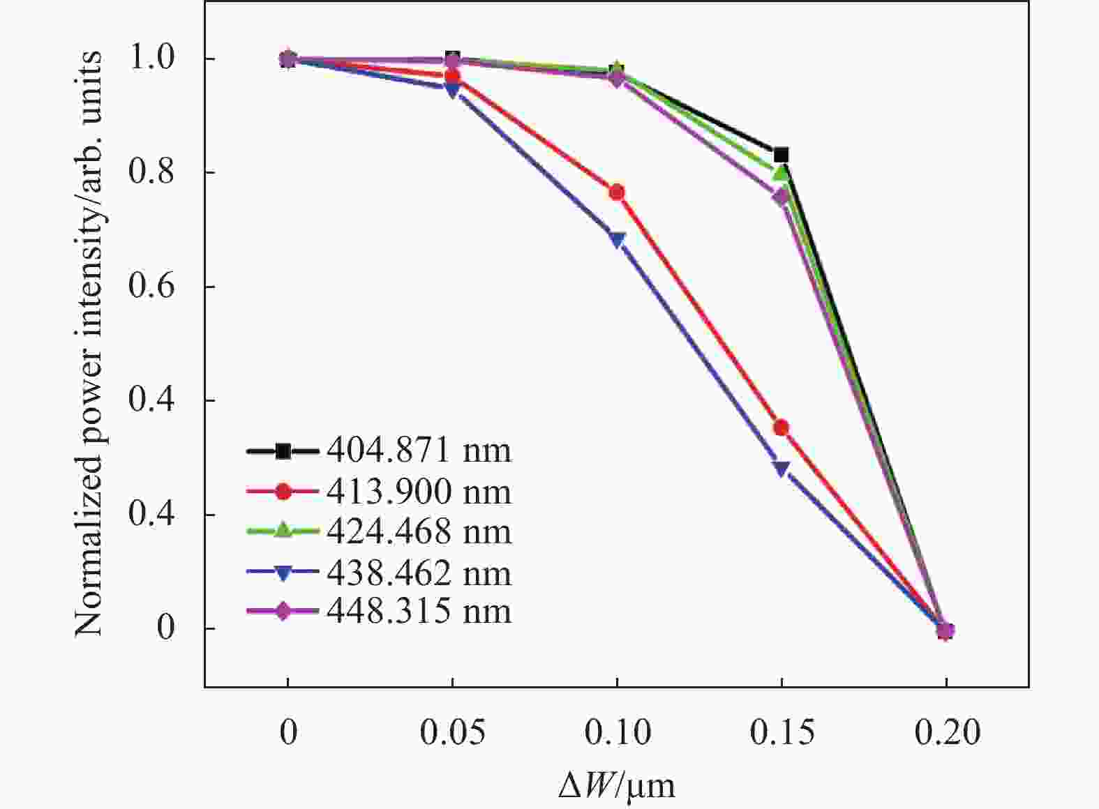
图 6 五个模式的峰值功率随内圆偏移量的变化的归一化曲线
Figure 6. The normalized peak power of the five modes as a function of the offset of the inner circle
-
通常通过干法刻蚀技术制备微盘激光器,其会在器件边缘引入非常多的侧壁缺陷,从而使侧壁的非辐射复合增加,电流注入边缘时,其很难达到粒子数反转实现增益[19]。因此,进一步研究了在内圆直径为0.4 μm时,通过增加外圆边缘处的无增益区域来模拟微盘边缘的缺陷厚度对蓝光微盘激光器性能的影响,将外圆与微盘边缘的距离设为0、50、100、150 nm,其功率随波长的变化曲线如图7所示,其中引入$ W $代表无增益外环的宽度,即微盘边缘缺陷厚度。从图中可以看出,随着$ W $的增加,五个模式的功率均快速减小,且当$ W $为100 nm后,一阶模式几乎消失。需要注意的是,由于无法获得缺陷带来的吸收具体数值,故该工作直接设置是常规材料的吸收。通常情况下刻蚀损伤引起的吸收会比文中设置的无增益区吸收更大,会对输出功率影响更剧烈。
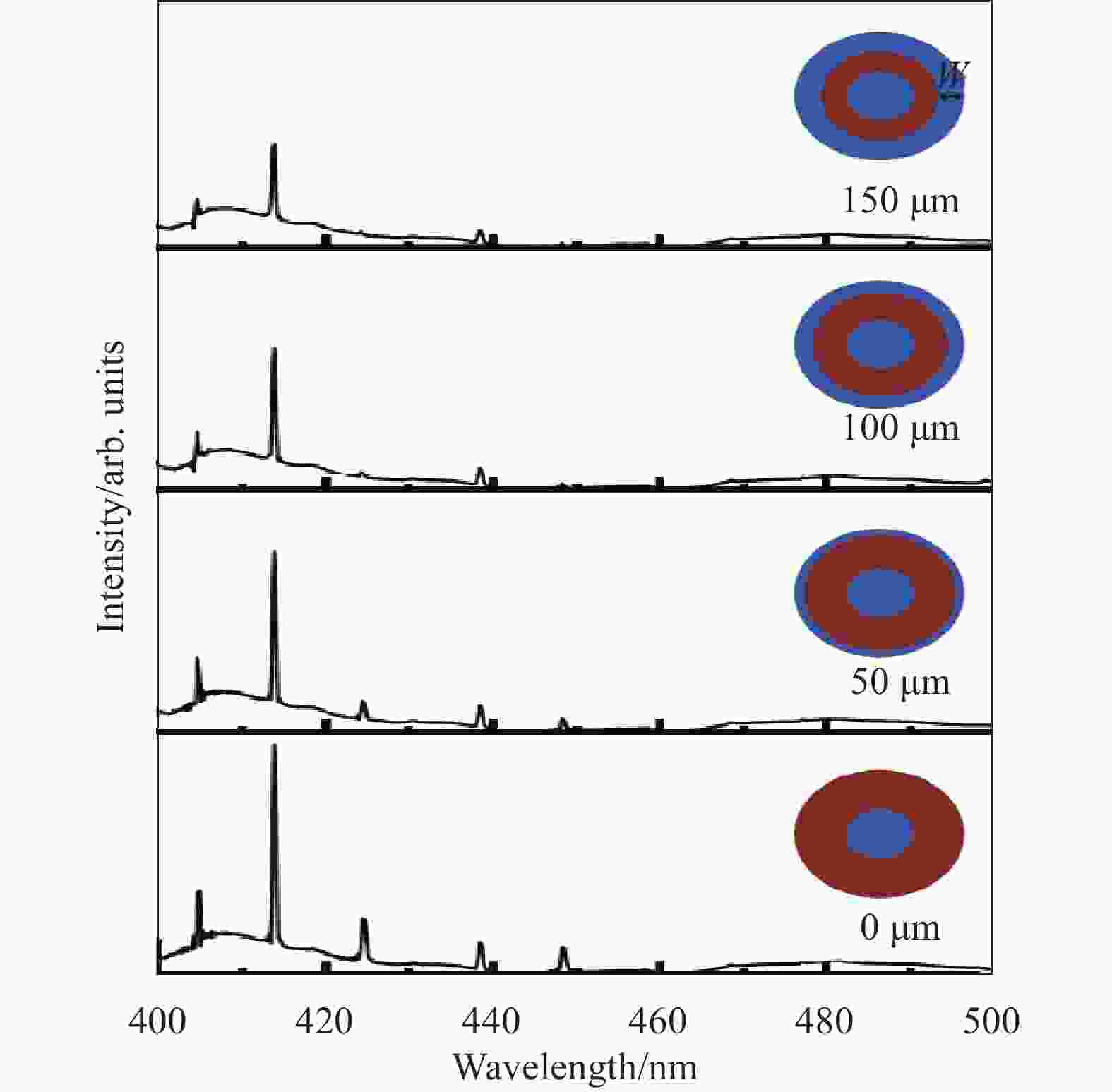
图 7 外圆与微盘边缘距离增加时,FDTD模拟了器件的共振 (插入图为增益设置示意图,红色区域材料为洛伦兹增益材料,蓝色区域材料为无增益材料)
Figure 7. Optical resonances for devices with different no-gain outer ring (The inset figure: a schematic diagram of the gain setting. The Lorentz gain material and no gain material are set in the red and blue region)
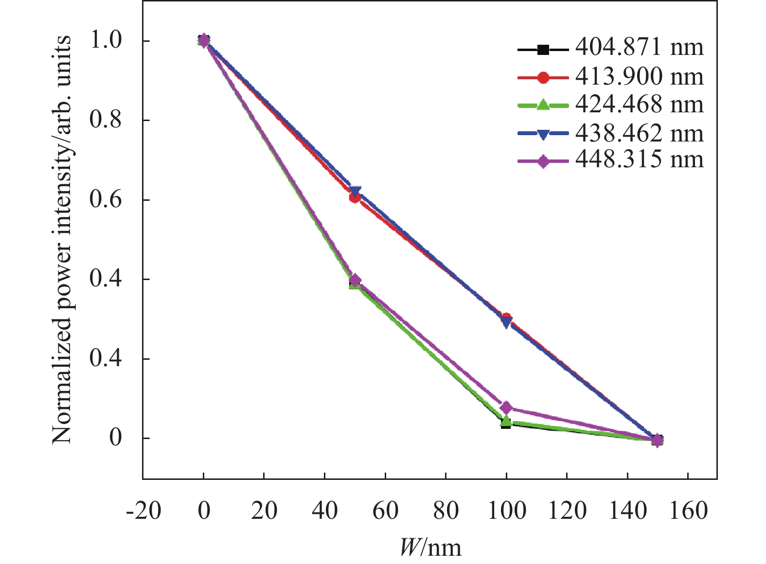
图8表示了图7中五个模式的峰值功率随$ W $取值不同的归一化曲线。从图中可以看出,随着$ W $的取值越来越大,一阶模式功率下降的速度比二阶模式快。这是由于一阶模式更加靠近微盘腔的边缘,其与边缘无增益区域重合率更大,从而导致一阶模式的损耗增加更大,因此一阶模式峰值的功率会下降得较快。综上所述,在实际制备中,应该尽量减小微盘侧壁的缺陷厚度,以提高微盘激光器的一阶模式的激射,如果缺陷区域超过50 nm,微盘中主要激射的将主要是二阶模式。

图 8 五个模式的峰值功率随无增益外环宽度变化的归一化曲线
Figure 8. Normalized peak power of the five modes as a function of the width of no-gain outer ring
-
文中利用FDTD从三个方面分析增益分布对蓝光微盘激光器性能的影响,并且得出电流阻挡层的边缘与微盘边缘距离为0.6 μm是最好的,如果距离太大,其中间注入的电流引起的增益对整个激光器的功率没有贡献;反之,如果距离太小,其将增加微盘激光器的吸收,从而增加激光器的阈值,减少激光的功率。其次,如果由于光刻精度导致电流阻挡层偏移时,其将增加激光器的吸收,减少激光器功率,尤其是对二阶模式的功率有重要影响;而如果是由于刻蚀缺陷引起边缘无增益区域增加,其也将明显降低激光功率,而且一阶模式的峰值功率比二阶模式减小得更加迅速。文中所得到的一系列研究结果对于微盘激光器的制备和设计有着重要的参考意义。
Effect of gain distribution on mode distribution and luminescence power of GaN-based blue microdisk lasers
-
摘要: 通过FDTD仿真模拟计算,文中系统地研究了电流阻挡作用对GaN基蓝光激光器增益分布和光学性能的影响,发现回音壁激光模式主要在靠近微盘边缘1.5个波长范围谐振,因此,如果电流阻挡层面积太小,无法最大化减小激光器电流阈值;如果面积太大,回音壁激光模式与无增益区存在耦合效应,从而减少激光功率。另外,随着无增益区域向微盘边缘发生偏移,各个激光模式输出的峰值功率均下降,其中二阶模式峰值功率比一阶模式下降得更加显著,这主要是由于二阶模式分布范围更接近微盘中心区域。同时,进一步发现如果在微盘激光器的仿真模型中引入侧壁缺陷,则将导致边缘无法形成增益区,相比于二阶模式而言,一阶模式的发光功率随侧壁缺陷区域增加而下降的幅度更为显著,这主要是由于一阶模式分布范围更接近微盘边缘。Abstract:
Objective The GaN-based microdisk laser based on whispering-gallery modes (WGMs) has the characteristics of high power, low threshold and small size. It has a wide-ranging application prospects and is needed in many fields such as optoelectronic integration, biomedicine and data transmission. However, due to the lack of conductive substrates and poor material grown quality, GaN-based microdisk lasers have long been dominated by light-injected microdisk devices. To achieve an electrically-driven GaN-based microdisk laser, a current block layer is typically introduced in the central region of the microdisk laser. This allows for injection of current only at the edge of the microdisk, resulting in that the low threshold laser output can be achieved, and the heat generation in the central region can be well suppressed. Although the effect of the central current block layer has been reported, there is a lack of sufficient reports on the effect of current block layer size on the microdisk laser and its design guidelines. In this paper, the effect of the gain distribution affected by the current block layer design on the performance of blue laser is systematically investigated. Methods According to the structure of the reported blue microdisk laser, the device structure of this study is designed (Fig.1(a)). The gain material in the active region is set as the Lorentz gain material, the real and imaginary part curves of the refractive index are obtained by setting the material parameters (Fig.1(b)-(c)). The Finite-Difference Time-Domain simulation (FDTD) is used to analyze the effect of the gain distribution on the performance of the blue laser. The no-gain circle region represents the area where current is unable to inject due to the presence of current block layer Results and Discussions Firstly, the performance of the microdisk laser is studied by changing the diameter of no-gain circle region, and the resonance of the device is simulated by FDTD (Fig.3). The results show that there are five distinct modes, all of which exhibit a gradually decrease in power as the diameter of the no-gain circle increases. In addition, the total power output exhibits a decreasing trend with the increase of the diameter of the no-gain circle region. Specifically, the total power first decreases slowly from 0 μm to 0.4 μm, followed by a sharp decrease beyond 0.4 μm (Fig.4). Therefore, when the diameter of no-gain circle is less than 0.4 μm, it will not significantly affect the output power and threshold gain of the laser. Secondly, by adjusting the offset of no-gain circle to align with device edge, the effect of space between no-gain circle and device edge on the performance of the microdisk laser is analyzed. The analysis results show that the powers of the five modes decrease as the no-gain circle gradually approaches to the edge of the device (Fig.5). And compared with the first-order mode, the peak power of the second-order mode decreases faster (Fig.6). Finally, the effect of edge defects on the performance of GaN-based micro laser is analyzed. The peripheral no-gain ring region represents the device sidewall defect area from the dry-etched process. The results show that the peak power of the five modes decreases rapidly with the increase of no-gain ring width (Fig.7). Moreover, when the no-gain ring width increases, the power of the first-order mode decreases faster than that of the second-order mode (Fig.8). This is due to the fact that the distribution range of the first-order mode is closer to the edge of the microdisk. Conclusions In this paper, FDTD is employed to investigate the effect of different gain distributions on the performance of blue microdisk lasers. The optimal distance between the edge of the current block layer and the edge of the microdisk is determined to be 0.6 μm. Too large distance will make some current injected in the middle not contribute to the power of the laser, resulting in increased threshold current and heat effects. Conversely, if it is too small, it will increase the absorption of the microdisk laser, thereby reducing the power of the laser. Moreover, if the current block layer is offset due to lithography, it will result in an increase in absorption in device and a reduction in the laser power, especially for the second-order mode. If the edge no-gain region expands due to the increased sidewall defects, the laser power will be significantly reduced, and the power of the first-order mode decreases more rapidly than that of the second-order mode. The results in this paper have significant reference value for the fabrication and design of microdisk lasers. -
图 1 (a) 蓝光微盘激光器仿真模型图;(b) 洛伦兹材料折射率实部曲线图;(c) 洛伦兹材料折射率虚部曲线图
Figure 1. (a) Simulation model of blue microdisk laser diode; (b) Real part of the refractive index; (c) Imaginary part of the refractive index of a Lorentz material
图 2 (a) 多量子阱层的侧视图;(b) 沿(a)图虚线处的截面图 (红色区域材料为洛伦兹增益材料,蓝色区域材料为无增益材料)
Figure 2. (a) Side view of QWs;(b) Top view for one QW (The Lorentz gain material and no gain material are set in the red and blue region in figure (b))
图 3 (a) 内圆直径不同时,FDTD模拟了器件的共振 (插入图为增益设置示意图,红色区域材料为洛伦兹增益材料,蓝色区域材料为无增益材料);激射波长为(b) 404.871 nm、(c) 413.9 nm、(d) 424.468 nm、(e) 438.462 nm、(f) 448.315 nm处的XY面强场分布图
Figure 3. (a) The FDTD simulation resonance of devices with different diameter for the inner circle (The inset figure: a schematic of the gain setting. The Lorentz gain material and no gain material are set in the red and blue region in figure (a)); The XY-cross section electrical field intensity distributions at (b) 404.871 nm, (c) 413.9 nm, (d) 424.468 nm, (e) 438.462 nm and (f) 448.315 nm
图 4 总功率随内圆直径的变化规律
Figure 4. The total output power as a function of diameter of inner circle
图 5 在直径为0.4 μm的内圆的偏移量不同时,FDTD模拟了器件的共振 (插入图为增益设置示意图,红色区域材料为洛伦兹增益材料,蓝色区域材料为无增益材料)
Figure 5. The FDTD simulation resonances of devices with 0.4 μm diameter inner circle and different offset (The inset figure: a schematic of the gain setting. The Lorentz gain material and no gain material are set in the red and blue region)
图 6 五个模式的峰值功率随内圆偏移量的变化的归一化曲线
Figure 6. The normalized peak power of the five modes as a function of the offset of the inner circle
图 7 外圆与微盘边缘距离增加时,FDTD模拟了器件的共振 (插入图为增益设置示意图,红色区域材料为洛伦兹增益材料,蓝色区域材料为无增益材料)
Figure 7. Optical resonances for devices with different no-gain outer ring (The inset figure: a schematic diagram of the gain setting. The Lorentz gain material and no gain material are set in the red and blue region)
图 8 五个模式的峰值功率随无增益外环宽度变化的归一化曲线
Figure 8. Normalized peak power of the five modes as a function of the width of no-gain outer ring
表 1 材料的折射率和吸收系数
Table 1. Index and absorption coefficient of the material
Material Index Absorption/m−1 n-GaN 2.471 1.0964×10⁻⁸ n-Al0.08Ga0.92N 2.49 9.6687×10⁻⁸ u-GaN 2.471 3.65467×10⁻⁹ In0.02Ga0.88N 2.53 2.6548×10⁻⁹ p-Al0.2Ga0.8N 2.44 1.0964×10⁻⁶ p-Al0.07Ga0.93N 2.496 9.6687×10⁻⁷ P-GaN 2.471 3.6547×10⁻⁸  下载: 导出CSV
-
[1] Alexander K, van Vaerenbergh T, Fiers M, et al. Excitability in optically injected microdisk lasers with phase controlled excitatory and inhibitory response [J]. Opt Express, 2013, 21(22): 26182-26191. doi: 10.1364/OE.21.026182 [2] Peter E, Senellart P, Martrou D, et al. Exciton-photon strong-coupling regime for a single quantum dot embedded in a microcavity [J]. Phys Rev Lett, 2005, 95(6): 067401. doi: 10.1103/PhysRevLett.95.067401 [3] Gil-santos E, Baker C, Nguyen D T, et al. High-frequency nano-optomechanical disk resonators in liquids [J]. Nat Nanotechnol, 2015, 10(9): 810-816. doi: 10.1038/nnano.2015.160 [4] Wang D, Zhu T, Oliver R A, et al. Ultra-low-threshold InGaN/GaN quantum dot micro-ring lasers [J]. Opt Lett, 2018, 43(4): 799-802. doi: 10.1364/OL.43.000799 [5] Xu X, Chen W, Zhao G, et al. Wireless whispering-gallery-mode sensor for thermal sensing and aerial mapping [J]. Light Sci Appl, 2018, 7(1): 62. doi: 10.1038/s41377-018-0063-4 [6] Mccall S L, Levi A F J, Slusher R E, et al. Whispering-gallery mode microdisk lasers [J]. Applied Physics Letters, 1992, 60(3): 289-291. doi: 10.1063/1.106688 [7] Feng M, He J, Sun Q, et al. Room-temperature electrically pumped InGaN-based microdisk laser grown on Si [J]. Opt Express, 2018, 26(4): 5043-5051. doi: 10.1364/OE.26.005043 [8] Wang J, Feng M, Zhou R, et al. GaN-based ultraviolet microdisk laser diode grown on Si [J]. Photonics Research, 2019, 7(6): B32-B35. doi: 10.1364/PRJ.7.000B32 [9] Wang J, Feng M, Zhou R, et al. Continuous-wave electrically injected GaN-on-Si microdisk laser diodes [J]. Opt Express, 2020, 28(8): 12201-12208. doi: 10.1364/OE.391851 [10] Wang J, Feng M, Zhou R, et al. Thermal characterization of electrically injected GaN-based microdisk lasers on Si [J]. Applied Physics Express, 2020, 13(7): 074002. doi: 10.35848/1882-0786/ab95f0 [11] Tang Y, Feng M, Zhao H, et al. Electrically injected GaN-on-Si blue microdisk laser diodes [J]. Opt Express, 2022, 30(8): 13039-13046. doi: 10.1364/OE.455620 [12] Feng M, Zhao H, Zhou R, et al. Continuous-wave current injected InGaN/GaN microdisk laser on Si (100) [J]. ACS Photonics, 2022, 28(8): 2208-2215. [13] Zhao H, Feng M, Liu J, et al. Performance improvement of GaN-based microdisk lasers by using a PEALD-SiO2 passivation layer [J]. Optics Express, 2023, 31(12): 20212-20220. doi: 10.1364/OE.493849 [14] Kuramoto M, Sasaoka C, Futagawa N, et al. Reduction of Internal loss and threshold current in a laser diode with a ridge by selective re-growth (RiS-LD) [J]. Phys Status Solidi, 2002, 192(2): 329-334. doi: 10.1002/1521-396X(200208)192:2<329::AID-PSSA329>3.0.CO;2-A [15] Efremov A A, Tarkhin D V, Bochkareva N I, et al. Determination of the coefficient of light attenuation in thin layers of light-emitting diodes [J]. Semiconductors, 2006, 40(3): 375-378. doi: 10.1134/S1063782606030225 [16] 王瑾. 硅衬底GaN基微盘激光器的设计与制备研究 [D]. 北京; 北京科技大学, 2020. Wang Jin. Design and fabrication of GaN-based microdisk lasers on Si substrate [D]. Beijing: University of Science and Technology Beijing, 2020. (in Chinese) [17] Zhu G, Li J, Li J, et al. Single-mode ultraviolet whispering gallery mode lasing from a floating GaN microdisk [J]. Opt Lett, 2018, 43(4): 647-650. doi: 10.1364/OL.43.000647 [18] Zhang Y, Li H, Li P, et al. Optically-pumped single-mode deep-ultraviolet microdisk lasers with algan-based multiple quantum wells on Si substrate [J]. IEEE Photonics Journal, 2017, 9(5): 1-8. [19] Tamboli A C, Haberer E D, Sharma R, et al. Room-temperature continuous-wave lasing in GaN/InGaN microdisks [J]. Nature Photonics, 2006, 1(1): 61-64. -

 点击查看大图

计量
- 文章访问数: 50
- HTML全文浏览量: 10
- PDF下载量: 12
- 被引次数: 0

