


-
作为信息化时代的新“视窗”,柔性显示已成为显示技术中革命性的新领域。柔性显示的实现能够使可折叠的电子报刊、画轴一样的电视和可穿戴的智能终端等有望成为现实。相比OLED有机材料体系,无机半导体具有更稳定的物理化学性质。然而晶态的无机薄膜并不具有良好的柔韧性,弯折后容易龟裂。因此,生长温度较低、具有较好柔韧性的非晶薄膜和纳米结构阵列成为无机柔性器件的合适选择。其中,基于纳米线阵列的柔性器件吸引了研究人员的广泛关注。纳米线的高单晶性有益于提高光发射器件中的载流子输运和复合效率,而且合成方法多样而柔和,可以直接生长在多种衬底上[1]。纳米线的微小尺寸极大降低了弯折状态下的应力,而阵列空隙可以一定程度上释放纳米线的应力,成为柔性器件研究新的突破方向[2-3]。
宽禁带半导体氧化锌(ZnO)是发展短波长发光和激光器件的理想材料[4-5],其激子束缚能高达60 meV,在室温下能够获得高效的激子发射,可以实现低阈值的激子激光器件。缺少成熟的p型掺杂技术限制了ZnO基发光器件的研究开发。目前大部分研究都关注于构建以ZnO作为有源层的异质结光发射器件。例如,与其他替代的成熟的p型半导体材料(如GaN等)结合构建p-n异质结。但这些p-n异质结器件的电致发光往往是来源于p型区一侧的发光或界面跃迁复合,ZnO高激子束缚能的优异特性并没有得到充分利用,更难以获得ZnO的激子属性的电泵浦激射。于是,另一种异质结器件,即金属-绝缘体-半导体(MIS)结构,吸引了更多研究人员的关注[5-6]。MIS异质结的势垒层可以有效限制半导体有源层中的载流子,避免了p-n异质结器件对发光来源的争议。早在20世纪70年代,研究人员就构建了氧化锌MIS结发光器件,在室温脉冲泵浦下,获得了ZnO的紫外电致发光。
另一方面,ZnO也是当下研究最多的纳米材料之一,尤其关于ZnO纳米线的合成与物性的研究不胜枚举。其中,低温水热合成方法应用最为广泛,通过优化生长条件可以实现纳米线阵列的可控生长[7-8]。在光电器件应用方面,ZnO纳米线具有许多得天独厚的优势。纳米ZnO的光学增益远大于体相和薄膜材料,纳米线异质结具有更高的注入效率和光萃取效率,因而ZnO纳米线光发射器件成为当下的研究热点[6,9]。ZnO的荧光光谱主要分为紫外波段的本征近带边发射和可见光波段的缺陷相关的深能级复合两部分。相比于体相材料,纳米线的高表面积体积比值容易产生更多的表面缺陷态。对于氧化锌材料来说,这些表面缺陷态(通常为深能级缺陷)对其发光性质的影响主要是会抑制紫外本征发射、增强可见区发光和非辐射复合。比如,ZnO纳米线长径比越大,表面效应越显著,可见区的深能级发射通常占据荧光谱主导。如果采用ZnO薄膜作为激活层,可以有效减少表面缺陷的影响,有利于提高器件稳定性。但晶态的ZnO薄膜并不具有良好的柔韧性,弯折状态下会在器件各膜层中产生不同的应力积累甚至断裂。为了提高一维纳米ZnO的光学性质,获得高效的紫外本征发射,最常用和有效的方法就是在纳米ZnO包覆一层钝化层,形成纳米异质结构。常用的包覆层材料有MgO、Al2O3、ZnS、TiO2、SiO2等氧化物和高分子聚合物(如聚乙烯等),其中氧化镁 (MgO)是应用较多的一种包覆层材料,通过构建ZnO/MgO异质结构,可以钝化ZnO纳米线表面的缺陷态,抑制深能级发射。此外,MgO具有良好的介电性质和更宽的带隙,可以直接作为MIS异质结器件的势垒层。
近年来,全无机铯铅卤化物钙钛矿材料(CsPbX3(X = I,Br,Cl)),因其优异的光学性质掀起了新的研究热潮[10]。CsPbX3纳米晶不仅可以通过控制量子点尺寸来实现带隙调制,还可以通过卤族元素组分调节(Cl/Br和Br/I的比例)获得不同的发射波长。即使纳米晶尺寸较大(9~10 nm)时量子限域效应变弱,仍能够获得蓝光发射,可以覆盖410~700 nm波长范围的整个可见光谱[11]。尤其出色的是,金属卤化物钙钛矿材料几乎没有带间缺陷态,CsPbX3纳米晶的发光量子产率可高达90%[12],而且由于合成中使用油胺和油酸作为表面活性剂,其中的烃基和胺类官能团可能会吸附在表面,CsPbX3量子点易于分散到各种非极性溶剂中,可以作为制备光电器件的特殊墨水;也可以沉积到任意基底上,容易与各种光电材料相溶混,有利于实现柔性器件。然而,目前基于钙钛矿量子点材料作为发光激活层的量子点LED器,均难以实现较高的电致发光效率,远远低于其荧光量子产率。因此,如果将钙钛矿量子点作为荧光层分散在纳米线阵列中,不仅可以实现可见波段的柔性发光器件,而且可以有效利用钙钛矿材料荧光效率的优异性质。
文中首先使用水热法可控合成了ZnO纳米线阵列,而后溅射沉积MgO包覆层,构建了ZnO/MgO纳米线阵列异质结构。在柔性锌箔衬底上构建了纳米线阵列MIS异质结原型发光器件,实现了源自ZnO纳米线的本征紫外电致发光和电泵浦激射。随后使用热注入法合成CsPbBr3&CsPbI3量子点,将钙钛矿量子点/PMMA饱和溶液旋涂分散到纳米线阵列中。采用MIS异质结作为短波长激发源、钙钛矿量子点作为荧光层,实现了柔性荧光型暖白光LED原型器件。
-
ZnO纳米线的合成工艺丰富多样,可以通过多种物理化学方法制备获得。水热法是一种低成本的绿色湿化学方法,通过前驱体浓度、反应时间、反应温度、活性剂和pH值等多种实验参数,可以实现对纳米线微观形貌的精细调控。实验研究了前驱体溶液浓度对于纳米线的表面形貌和光学性质等物性的影响。
-
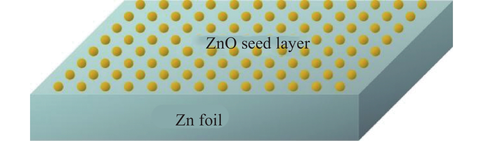
在水热制备ZnO纳米线阵列的过程中,在基片上预先沉积一层晶种层,有助于获得取向排列的纳米线,并且提高纳米线与基片之间连接的牢固度。同时,通过调控晶种的排布可以控制纳米线阵列的面密度。实验中采用锌箔作为柔性衬底,由于锌箔基片是多晶的,表面Zn晶粒的取向随机,因此,通过溅射方法在预清洗的基片表面沉积了一层ZnO纳米晶作为纳米线生长的晶种层,如图1所示。
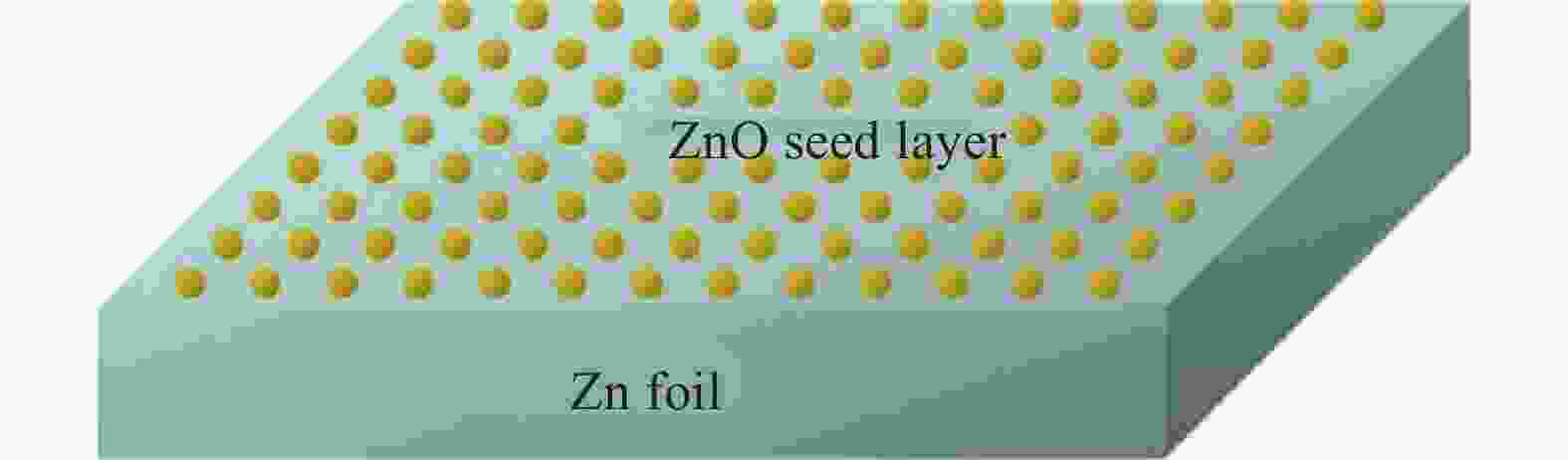
图 1 在锌箔上溅射沉积生长ZnO纳米晶种层的示意图
Figure 1. Schematic diagram of nano-ZnO seed layer grown by sputtering deposition on zinc foil
图2为锌箔上ZnO纳米晶种层的X射线衍射(XRD)图谱。从图中可以观察到一个明显的、尖锐的衍射峰,通过与标准JCPDS卡片对比,可知为ZnO纳米晶种层的(002)衍射峰,证实了ZnO晶种层为六角纤锌矿结构,并沿着c轴方向取向生长。

图 2 锌箔上ZnO纳米晶种层的X射线衍射谱
Figure 2. X-ray diffraction pattern of nano-ZnO seed layer on zinc foil
-
水热法合成ZnO纳米线是用Zn盐与碱性物质作为前驱体,在高温高压条件下完成化合反应。水热反应中,ZnO的锌离子来自于前驱体中锌盐,氧离子由前驱体碱性物质提供。实验中,选择二水乙酸锌和六次甲基四胺作为前驱体。将沉积了ZnO晶种层的锌箔基片放入反应釜内,随后将混合的前驱体溶液加入到反应釜中。前驱体溶液液面高度大约为反应釜内深度的2/3。水热反应温度为95 ℃,反应时间为150 min。反应完成取出基片后,用去离子水清洗样品表面,去除杂质残留。随后在450 ℃下烘烤30 min,去除样品中的有机杂质残留。
首先使用射频磁控溅射,在锌箔衬底上沉积了一层ZnO纳米晶作为纳米线的晶种层。如表1所示,实验中采用前驱体浓度分别为10 mmol/L、15 mmol/L和20 mmol/L,水热合成了ZnO纳米线阵列。采用扫描电子显微镜在不同放大倍率下表征了ZnO纳米线阵列的微观形貌,如图3所示。当前驱体溶液浓度为10 mmol/L时,纳米线的长径比更高、直径较细,而且纳米线顶部区域相比根部变得尖锐。随着前驱体浓度的增加,纳米线的直径明显随之增加,而长径比则相对减少。当前驱体溶液浓度为20 mmol/L时,纳米线顶端根部尺寸均匀,呈现出垂直基片方向的高度取向排列生长,并且具有更高的纳米线面密度,有利于在纳米线阵列表面沉积获得连续的介质包覆层构建异质结器件。
表 1 水热合成制备ZnO纳米线阵列的工艺参数
Table 1. Process parameters for hydrothermal synthesis of ZnO nanowire arrays
Temperature/℃ HMTA/mmol·L–1 Zinc acetate dihydrate/mmol·L–1 Time/h 95 10 10 2.5 95
9515
2015
202.5
2.5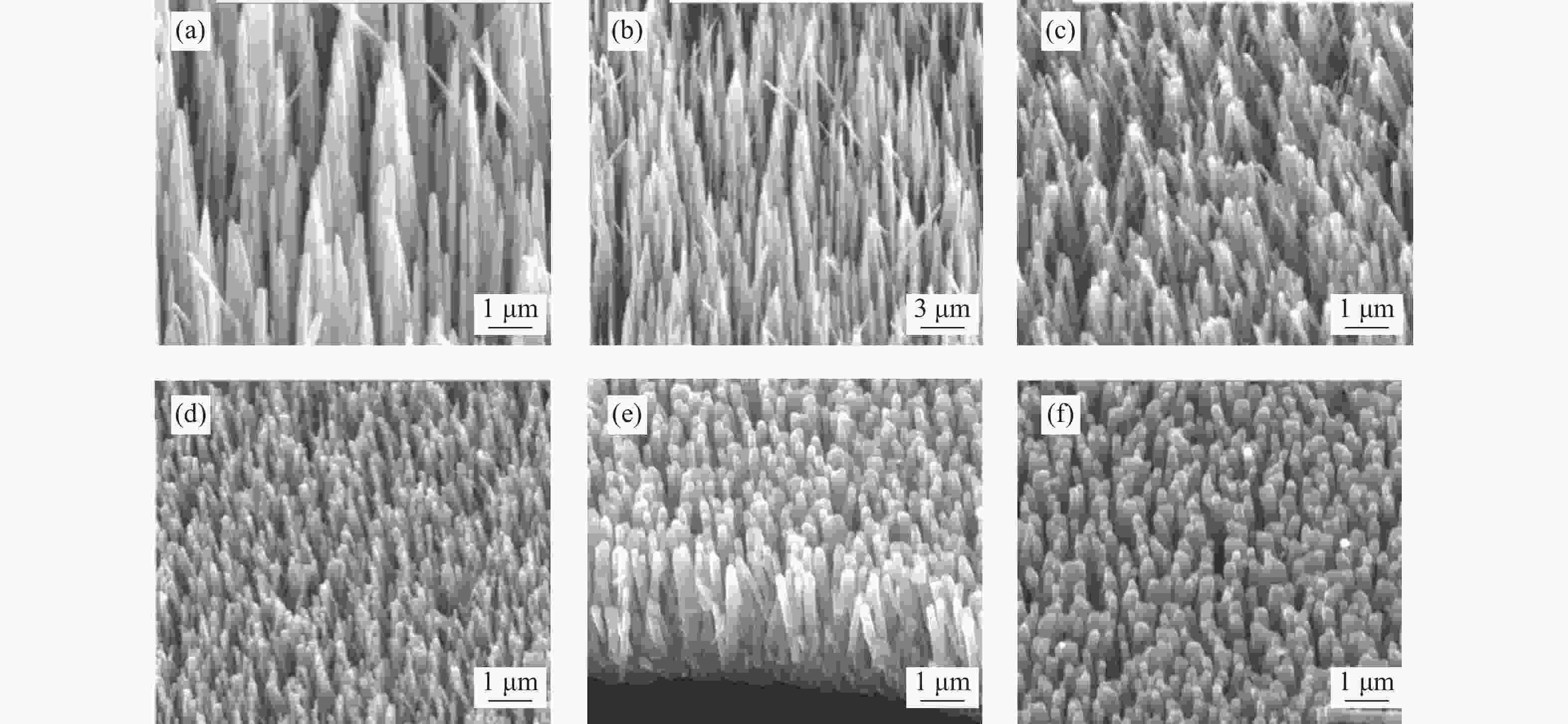
图 3 前驱体六次甲基四胺和二水醋酸锌浓度分别为10 mmol/L ((a)~(b))、15 mmol/L ((c)~(d))和20 mmol/L ((e)~(f))水热合成的ZnO纳米线阵列的扫描电子显微图像
Figure 3. Scanning electron microscope images of hydrothermal synthesized ZnO nanowire arrays with the concentrations of the precursor hexa methine group tetramine and zinc acetate dihydrate are 10 mmol/L ((a)-(b)), 15 mmol/L ((c)-(d)) and 20 mmol/L ((e)-(f))
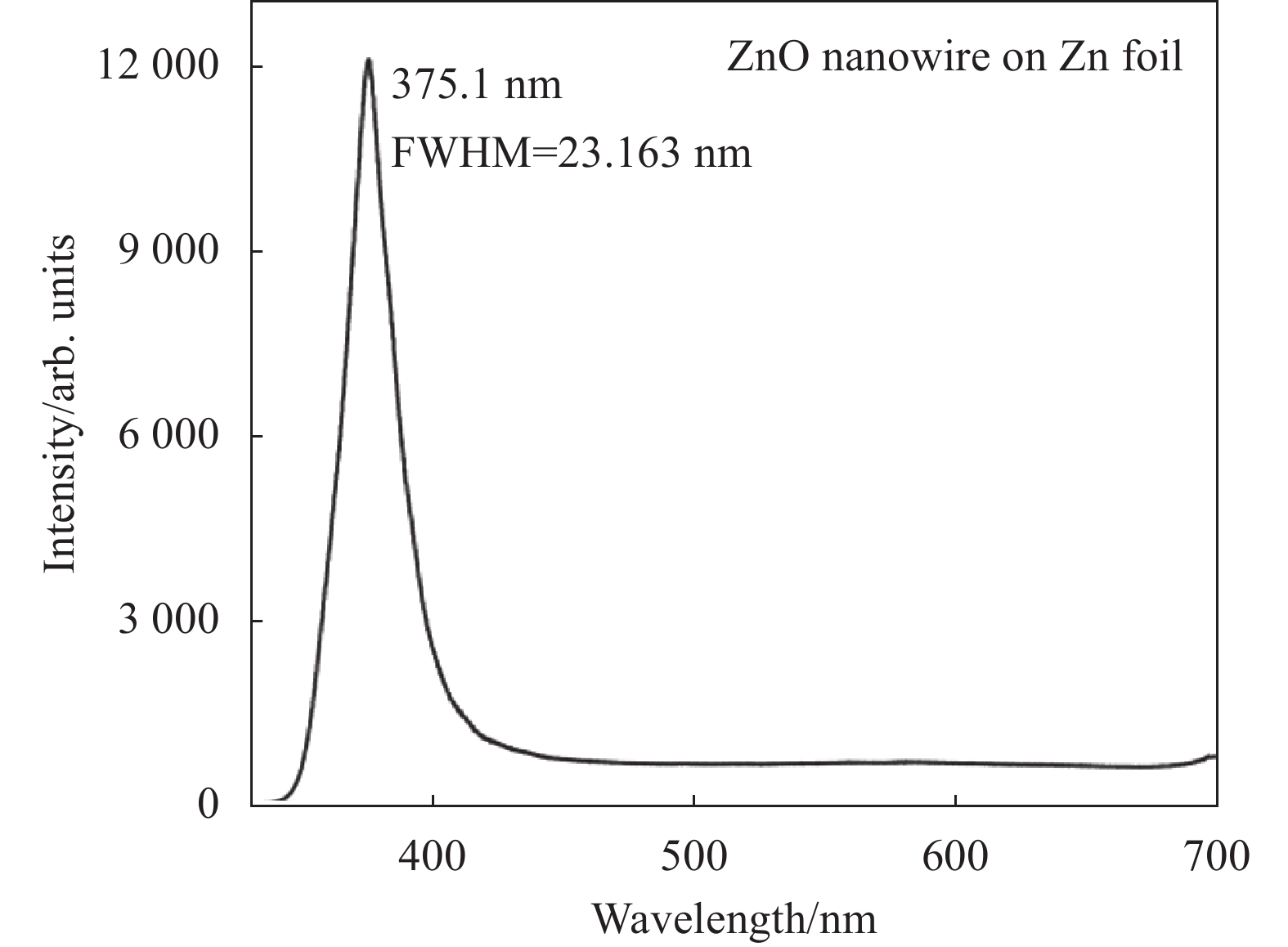
继续表征前驱体溶液浓度为20 mmol/L的ZnO纳米线阵列的光学性质,室温光致发光光谱如图4所示。在325 nm He-Cd激光器激发下,ZnO纳米线在375 nm附近呈现出较强的紫外发光峰,并且半高宽较窄,仅有~23 nm。这一紫外发光来自于ZnO的本征带边发射,可以归结为激子相关的跃迁复合。而在450~700 nm的可见波段,几乎观察不到ZnO惯常呈现的深能级缺陷相关的发射。ZnO纳米线阵列的光致发光光谱呈现出极高的紫外可见发光比,说明制备的纳米线具有很高的结晶质量和光学品质,进一步体现出纳米线的高单晶性。

图 4 锌箔上生长的ZnO纳米线阵列的光致发光光谱
Figure 4. Photoluminescence spectrum of ZnO nanowire arrays grown on zinc foil substrates
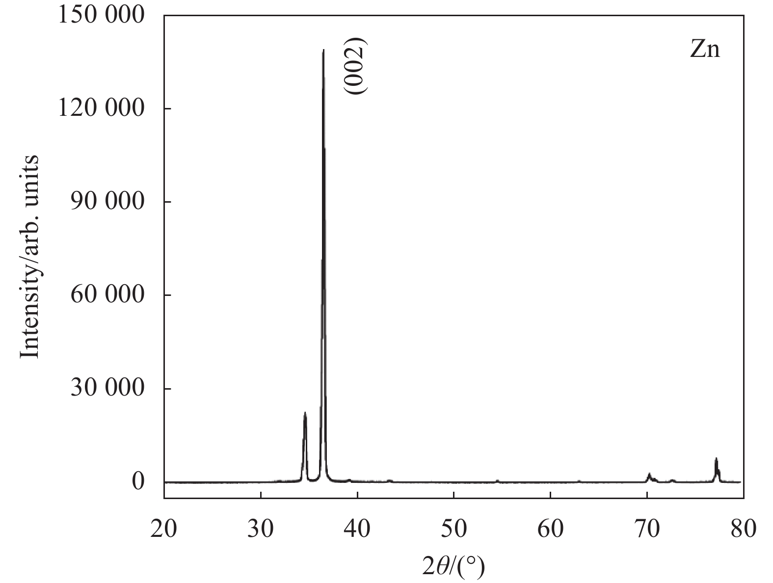
为了表征ZnO纳米线的结晶性质,对锌箔基片上水热合成的纳米线阵列进行X射线衍射测试。测试中采用2θ连续扫描模式,X射线功率为40 kV/100 mA,发散狭缝和防散射狭缝均为1°,限高狭缝为10 mm,接收狭缝为0.3 mm。扫描角度范围为30°~80°,扫描步长为0.02°。锌箔衬底上ZnO纳米线阵列的XRD图谱如图5所示。从图中可以观察到ZnO纳米线和锌箔基片的多个衍射峰,其中(002)峰明显居于主导,这与前文扫描电镜的表征结果相符,证实ZnO纳米线是垂直衬底表面择优取向生长。
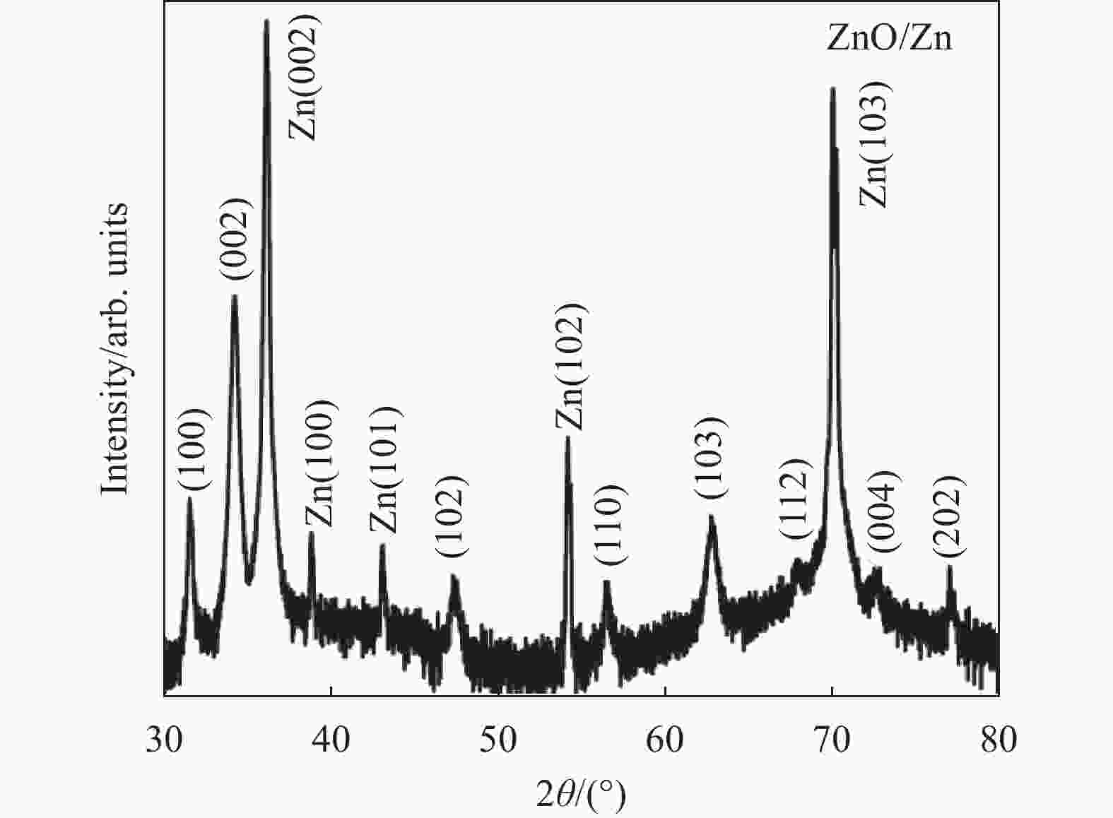
图 5 锌箔衬底上ZnO纳米线阵列的X射线衍射谱
Figure 5. X-ray diffraction pattern of ZnO nanowire arrays on zinc foil substrate
-
为构建MIS异质结器件,采用磁控溅射技术在ZnO纳米线阵列表面沉积了MgO膜层。MgO膜层的生长参数:靶基距为80 mm,反应温度为300 ℃,MgO靶功率为75 W,氧氩比值为2∶1,生长时间为2 h,压强为2 Pa。扫描电镜照片如图6所示,可以看出,ZnO纳米线阵列面密度较高,有利于在阵列顶端表面形成连续的膜层,而由于纳米线间的遮蔽效应,溅射到纳米线阵列的MgO粒子无法包覆纳米线根部的表面,因此,仅在纳米线的顶部区域形成了共轴生长包覆。
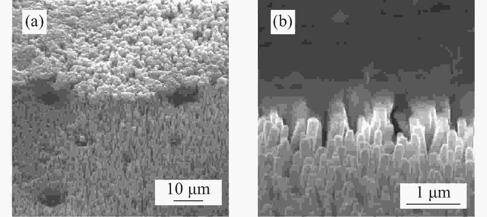
图 6 沉积MgO膜层的ZnO纳米线阵列的扫描电镜照片
Figure 6. Scanning electron microscopy photos of ZnO nanowire arrays deposited with MgO film layers
在ZnO纳米线阵列顶端沉积包覆了MgO介电层后,表征了ZnO/MgO纳米线阵列异质结构的结晶性质,如图7所示。XRD测试的过程和条件与之前完全相同。与标准 JCPDS卡片对比,不仅可以观察到ZnO纳米线和锌箔基片的衍射峰,同时观察到了立方相MgO的(200)衍射峰,溅射沉积的MgO膜层具有较好的结晶性质。

图 7 ZnO/MgO纳米线阵列异质结构的X射线衍射谱
Figure 7. X-ray diffraction pattern of ZnO/MgO nanowire arrays heterostructure
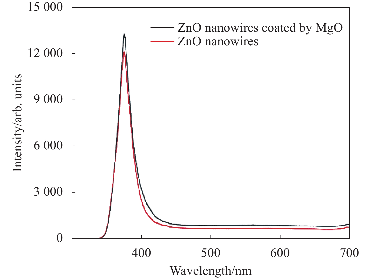
考虑到激发光源的透射深度,光致发光光谱的表征探测区域主要在纳米线阵列的顶端,与MIS异质结器件电致发光区域一致,均集中在ZnO/MgO界面区域附近。该器件结构中对ZnO纳米线阵列光致发光光谱的表征可以较大程度上反映表面和界面缺陷态对器件发光性能的影响。因此,继续对比表征了未包覆和包覆了MgO膜层的ZnO纳米线阵列的发光性质。实验中,发光光谱采用激光显微共聚焦光谱仪测试,在光致发光测试之前,先通过显微镜放大观察选定样品表面微米级区域。两次光谱在完全相同的条件下测试,激发光源入射光的波长、光斑尺寸和激发功率等所有配置均保持一致。因此,两次发光光谱中对发光强度的对比在一定程度上可以反映样品发光的强弱。如图8所示,沉积了MgO膜层后,ZnO纳米线阵列的紫外发光峰位和线宽以及深能级发射几乎没有变化。相比未包覆的纳米线阵列,沉积MgO膜层后,ZnO的紫外本征发射提高了~10.3%。考虑到包覆了MgO膜层的样品,激发光源入射光和纳米线阵列荧光均会受到MgO层的反射逸散损耗,因此,沉积MgO膜层后纳米线阵列的实际发光强度应比测试值更高,说明MgO膜层的包覆有效钝化了ZnO纳米线的表面缺陷和非辐射复合中心,进而提高了纳米线的辐射复合效率。

图 8 未包覆和包覆了MgO膜层的ZnO纳米线阵列的光致发光光谱
Figure 8. Photoluminescence spectra of ZnO nanowire arrays uncoated and coated with MgO film layers
-
采用热蒸发方法,利用掩膜技术,在 MgO膜层表面沉积了直径1 mm的 Au电极。构建了基于ZnO/MgO纳米线阵列异质结构的 MIS结光发射原型器件。纳米线阵列MIS异质结器件的结构示意图及实物照片如图9所示。

图 9 ZnO/MgO纳米线阵列MIS结光发射器件结构示意图 (a)和实物照片 (b)
Figure 9. Structural schematic diagram (a) and photo (b) of ZnO/MgO nanowire array MIS junction light emitting devices
测试了不同正向偏压下ZnO纳米线异质结柔性器件的电致发光光谱,如图10 (a)所示,与光致发光光谱相一致,纳米线发光器件在不同偏压下均展现出纯净的紫外发射,未观察到可见区的深能级缺陷相关的发射。在2.1 V偏压60 mA的低注入下,器件的电致发光主要表现为较弱的自发辐射。而随着电注入的增加,在自发辐射的发光峰上叠加出现了尖锐的窄缝,表明出现了受激辐射。从图10(b)中可以看到,当正向偏压增加时,MIS结器件的发光强度呈现出明显的超线性变化,体现出激光发射的阈值特性,进一步证实ZnO纳米线器件实现了电泵浦激光。而不同电注入下,电致发光光谱中激光谐振峰的峰位表现出随机变化,表明ZnO纳米线器件的电泵浦激射为随机模式的激光[5-6]。由于锌箔衬底和ZnO之间可以形成良好的欧姆接触,进一步提高了纳米线器件的载流子注入效率,因此,柔性发光器件在很低的正向偏压下获得了高效的电泵浦紫外随机激光。

图 10 (a) 纳米线异质结柔性器件的电致发光光谱及(b) 电致发光强度随正向偏压的变化关系
Figure 10. (a) Electroluminescence spectra of nanowire heterojunction flexible devices and (b) the relationship between the intensity of electroluminescence and the forward bias voltage
-
实验中,使用PbBr2、PbI2、Cs2CO3、油酸和十八烯醇作为前驱体,采用热注入法制备了CsPbBr3和CsPbI3钙钛矿量子点。
CsPbBr3和CsPbI3量子点的透射电镜照片和光致发光光谱分别如图11和图12所示。可以看出,钙钛矿量子点均为立方体结构,表现出良好的尺寸均一性和高度的单分散性;CsPbBr3和CsPbI3量子点均表现出单一的接近高斯线形的荧光峰。两种量子点荧光分别位于绿光波段(峰值波长为531.4 nm)和红光波段(峰值波长为619 nm),并且量子点的荧光均体现出较好的单色性,线宽仅为~19 nm。
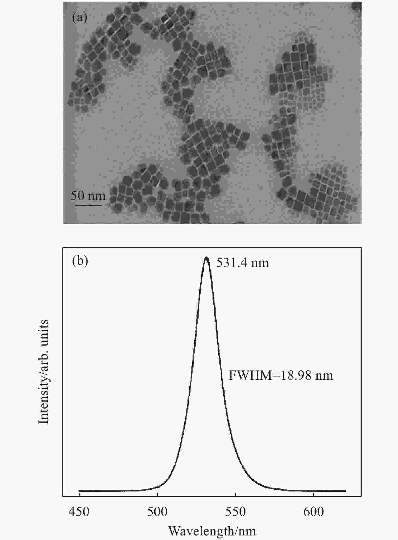
图 11 (a) CsPbBr3量子点的透射电镜照片及(b) CsPbBr3量子点的光致发光光谱
Figure 11. (a) Transmission electron microscopy photos of CsPbBr3 quantum dots and (b) photoluminescence spectrum of CsPbBr3 quantum dots
-
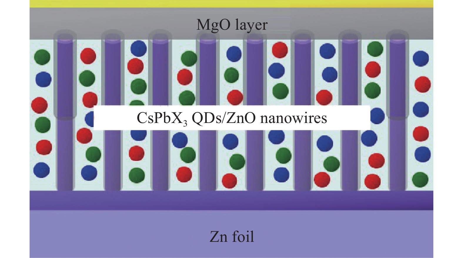
将CsPbBr3&CsPbI3量子点/PMMA饱和溶液旋涂分散到ZnO纳米线阵列中,形成封装膜层。采用MIS异质结作为短波长激发源,钙钛矿量子点作为荧光层,构建实现柔性荧光型LED原型器件,如图13所示。
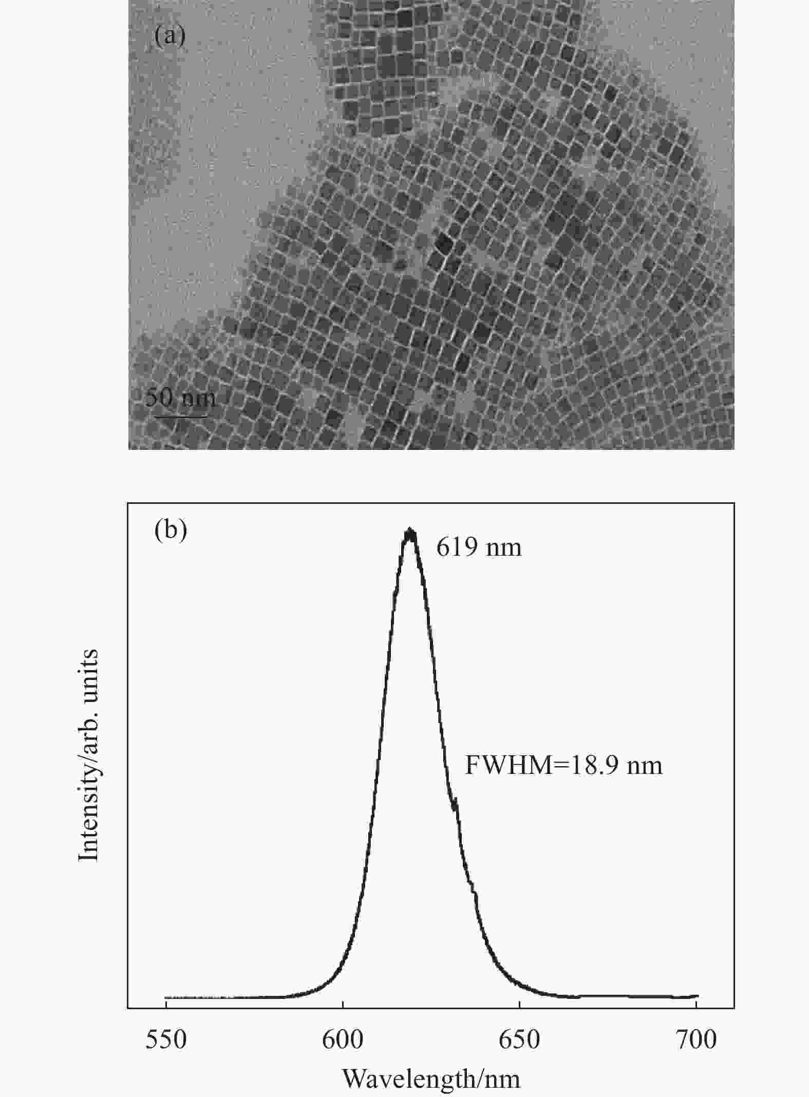
图 12 (a) CsPbI3量子点的透射电镜照片及(b) CsPbI3量子点的光致发光光谱
Figure 12. (a) Transmission electron microscopy photos of CsPbI3 quantum dots and (b) photoluminescence spectrum of CsPbI3 quantum dots
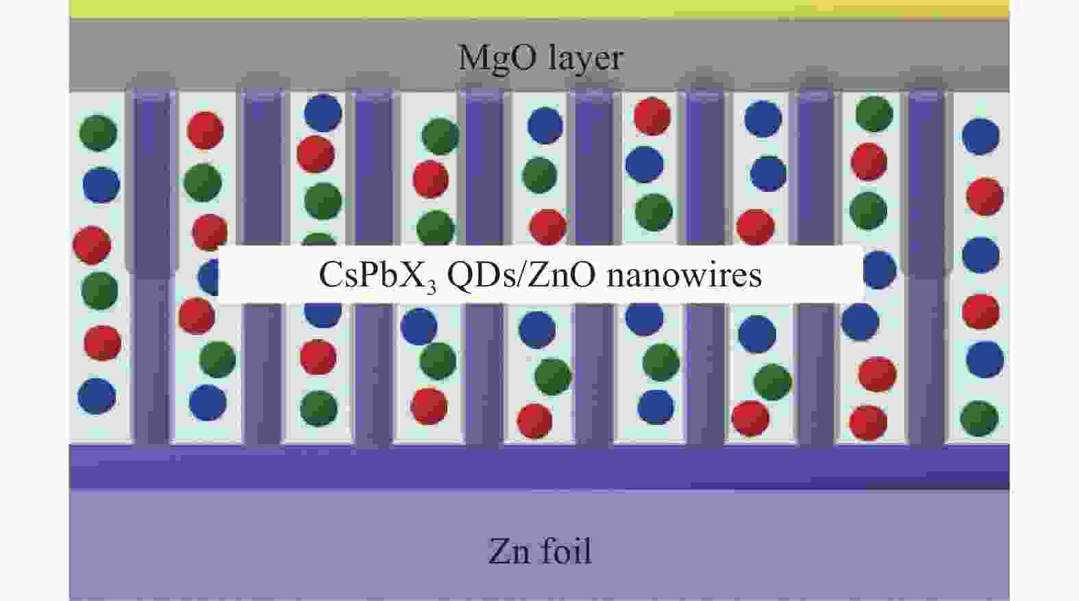
图 13 ZnO纳米线/CsPbX3量子点复合体系柔性发光器件示意图
Figure 13. Schematic diagram of ZnO nanowire/CsPbX3 quantum dots composite flexible light-emitting device
在室温大气压环境中,测试了6.2 V正向偏压下ZnO纳米线/钙钛矿量子点复合体系柔性光发射器件的电致发光。纳米线/量子点复合体系柔性光发射器件的电致发光光谱和CIExy色坐标图如图14所示。器件的电致发光光谱主要呈现出紫外和可见区两个包络,其中紫外波段发光是来自于ZnO纳米线MIS异质结的电致发光。而可见区较宽的发光包络(FWHM~123.8 nm)可以归结为纳米线异质结激发CsPbBr3&CsPbI3量子点产生的荧光。通过分峰拟合,可以得到三个子峰的峰值波长分别位于389.8 nm、531.4 nm和619 nm,与前文纳米线MIS结电致发光和量子点光致发光峰位高度契合。进一步分析了各发光子峰的积分强度比例分别为12.30%、63.98%和23.72%。由此可知,纳米线/量子点复合体系柔性发光器件中绿光占比最多,红光和蓝紫光比例较少。将电致发光光谱转换色坐标为(0.3498,0.4245),换算色温为5060 K,器件呈现出偏暖白光。后续研究中可以进一步调控量子点和纳米线的浓度比例,以及加入CsPbCl3蓝光量子点,实现高显色性白光器件。

图 14 纳米线/量子点复合体系柔性光发射器件的电致发光光谱和CIExy色坐标图
Figure 14. Electroluminescence spectra of nanowire/quantum dots composite flexible light-emitting device and CIExy chromatic coordinate diagram
-
在锌箔柔性衬底上制备合成了ZnO/MgO纳米线阵列异质结构,并构建了MIS结光发射原型器件。通过改变水热合成的前驱体浓度,实现了面密度合适的ZnO纳米线阵列的可控合成。MgO膜层的沉积包覆不仅形成了连续膜层,而且有效钝化了纳米线表面的非辐射复合中心,进一步提高了ZnO纳米线的紫外本征发射。在纳米线阵列柔性异质结器件中,实现了源自ZnO纳米线的紫外电致发光和电泵浦激射。随后采用热注入法制备合成了CsPbBr3&CsPbI3钙钛矿量子点,将量子点/PMMA饱和溶液旋涂分散到ZnO纳米线阵列中。采用MIS异质结作为短波长激发源、钙钛矿量子点作为荧光层,构建实现了柔性荧光型暖白光LED原型器件。该研究为柔性发光和显示探索了全新的发展思路。
Low-dimensional flexible light-emitting device based on quantum dots & nanowire composite
-
摘要: 柔性自发光器件是当前照明和显示领域的前沿课题。相比有机发光二极管,无机半导体具有更稳定的物理化学性质,但晶态无机薄膜不具有良好柔韧性,因此,低维纳米线阵列结构成为柔性器件研究新的突破方向。铯铅卤化物钙钛矿量子点具有高发光量子产率,将钙钛矿量子点作为荧光层分散在纳米线阵列中,可以利用钙钛矿材料的高荧光效率,实现可见波段柔性器件。首先制备了氧化锌 (ZnO)/氧化镁 (MgO)纳米线阵列异质结构,在柔性锌箔基片上构建了金属/绝缘体/半导体异质结光发射器件,实现了源自ZnO纳米线的本征紫外发射和电泵浦紫外随机激光。进而采用纳米线异质结作为短波长激发源、钙钛矿量子点作为荧光层,实现了柔性荧光型暖白光原型器件。Abstract:
Objective Flexible self-luminescent devices are the frontier subject in the field of illumination and display. Compared to organic light-emitting diodes, inorganic semiconductors offer more stable physical and chemical properties. However, crystalline inorganic films do not have good flexibility and are easy to crack after bending. Low-dimensional nanowire array structures have become a new breakthrough in the research of flexible devices. Wide bandgap semiconductor zinc oxide (ZnO) is an ideal material for developing short wavelength luminescence and laser devices. ZnO is also one of the most researched nanomaterials currently. Recently, all inorganic cesium lead halide perovskite materials (CsPbX3 (X=I, Br, Cl)) have sparked a new research boom due to their excellent optical properties. Cesium lead halide perovskite quantum dots have high luminescent quantum yields. By dispersing perovskite quantum dots as fluorescent layers in nanowire arrays, the high fluorescence efficiency of perovskite materials can be utilized to achieve visible band flexible devices. Methods ZnO nanowire array was prepared by hydrothermal synthesis method. Zinc foil was used as a flexible substrate. Due to the polycrystalline nature of the zinc foil substrate and the random orientation of surface Zn grains, nano ZnO layer was deposited on the pre-cleaned substrate surface by sputtering method as the seed layer for nanowire growth (Fig.1). In order to construct MIS heterojunction devices, MgO layer was deposited on the surface of ZnO nanowire arrays by magnetron sputtering. Au electrode with a diameter of 1 mm was deposited on the surface of MgO layer using thermal evaporation method and mask technology. The MIS junction light emitting device based on ZnO/MgO nanowire array heterostructure was constructed (Fig.9). Then, CsPbBr3&CsPbI3 perovskite quantum dots were prepared by thermal injection method. Lastly, CsPbBr3&CsPbI3 quantum dots/PMMA saturated solution were spin coated and dispersed into the ZnO nanowire array to form a packaging layer. Using MIS heterojunction as a short wavelength excitation source and perovskite quantum dots as a fluorescent layer, a flexible fluorescent LED prototype device is constructed (Fig.13). Results and Discussions As the concentration of precursor solution is 20 millimoles per liter, the size of the top and root of the nanowire is uniform, showing a highly oriented growth perpendicular to the substrate direction (Fig.3). ZnO nanowires exhibit a strong ultraviolet emission peak near 375 nm with a narrow width of ~23 nm, which can be attributed to exciton related transition recombination (Fig.4). In the visible wavelength range of 450-700 nm, the emission related to deep level defects commonly observed in ZnO was almost invisible. The photoluminescence spectra of ZnO nanowire arrays exhibit a high UV visible luminescence ratio, indicating that the prepared nanowires have high crystal and optical quality, further reflecting the high crystallinity of the nanowires. After depositing the MgO film layer, the UV emission peak position, line width, and deep level emission of the ZnO nanowire array remained almost unchanged. Compared to the uncoated nanowire array, the UV intrinsic emission of ZnO increased by ~10.3% after depositing MgO layer (Fig.8). Nanowire light-emitting devices exhibit pure ultraviolet emission under different bias voltages, and no deep level defect related emission in the visible region is observed. Electrically pumped UV random lasing was realized under very low forward bias voltage from this flexible light-emitting device (Fig.10). As to the flexible light-emitting devices of nanowire/quantum dot composite system, the proportion of green light is larger than red light and blue light (Fig.14). Therefore, the device exhibits warm white light. Conclusions In this work, ZnO/MgO nanowire array heterostructures were prepared and synthesized on flexible zinc foil substrate, and MIS junction light-emitting prototype device was constructed. By changing the concentration of precursor in hydrothermal synthesis, controllable synthesis of ZnO nanowire arrays with appropriate surface density was achieved. The deposition of MgO not only formed a continuous coating layer, but also effectively passivated the non radiative recombination centers on the nanowire surface, further improving the UV intrinsic emission of ZnO nanowires. In this flexible heterojunction devices of nanowire arrays, ultraviolet electroluminescence and electrically pumped lasing from ZnO nanowires have been achieved. Subsequently, CsPbBr3&CsPbI3 perovskite quantum dots were synthesized using thermal injection method, and the quantum dots/PMMA saturated solution were spin coated and dispersed into ZnO nanowire arrays. A flexible fluorescent warm white LED prototype device was constructed using MIS heterojunction as a short wavelength excitation source and perovskite quantum dots as a fluorescence layer. This paper explores new development ideas for flexible luminescence and display. -
图 1 在锌箔上溅射沉积生长ZnO纳米晶种层的示意图
Figure 1. Schematic diagram of nano-ZnO seed layer grown by sputtering deposition on zinc foil
图 2 锌箔上ZnO纳米晶种层的X射线衍射谱
Figure 2. X-ray diffraction pattern of nano-ZnO seed layer on zinc foil
图 3 前驱体六次甲基四胺和二水醋酸锌浓度分别为10 mmol/L ((a)~(b))、15 mmol/L ((c)~(d))和20 mmol/L ((e)~(f))水热合成的ZnO纳米线阵列的扫描电子显微图像
Figure 3. Scanning electron microscope images of hydrothermal synthesized ZnO nanowire arrays with the concentrations of the precursor hexa methine group tetramine and zinc acetate dihydrate are 10 mmol/L ((a)-(b)), 15 mmol/L ((c)-(d)) and 20 mmol/L ((e)-(f))
图 4 锌箔上生长的ZnO纳米线阵列的光致发光光谱
Figure 4. Photoluminescence spectrum of ZnO nanowire arrays grown on zinc foil substrates
图 5 锌箔衬底上ZnO纳米线阵列的X射线衍射谱
Figure 5. X-ray diffraction pattern of ZnO nanowire arrays on zinc foil substrate
图 6 沉积MgO膜层的ZnO纳米线阵列的扫描电镜照片
Figure 6. Scanning electron microscopy photos of ZnO nanowire arrays deposited with MgO film layers
图 7 ZnO/MgO纳米线阵列异质结构的X射线衍射谱
Figure 7. X-ray diffraction pattern of ZnO/MgO nanowire arrays heterostructure
图 8 未包覆和包覆了MgO膜层的ZnO纳米线阵列的光致发光光谱
Figure 8. Photoluminescence spectra of ZnO nanowire arrays uncoated and coated with MgO film layers
图 9 ZnO/MgO纳米线阵列MIS结光发射器件结构示意图 (a)和实物照片 (b)
Figure 9. Structural schematic diagram (a) and photo (b) of ZnO/MgO nanowire array MIS junction light emitting devices
图 10 (a) 纳米线异质结柔性器件的电致发光光谱及(b) 电致发光强度随正向偏压的变化关系
Figure 10. (a) Electroluminescence spectra of nanowire heterojunction flexible devices and (b) the relationship between the intensity of electroluminescence and the forward bias voltage
图 11 (a) CsPbBr3量子点的透射电镜照片及(b) CsPbBr3量子点的光致发光光谱
Figure 11. (a) Transmission electron microscopy photos of CsPbBr3 quantum dots and (b) photoluminescence spectrum of CsPbBr3 quantum dots
图 12 (a) CsPbI3量子点的透射电镜照片及(b) CsPbI3量子点的光致发光光谱
Figure 12. (a) Transmission electron microscopy photos of CsPbI3 quantum dots and (b) photoluminescence spectrum of CsPbI3 quantum dots
图 13 ZnO纳米线/CsPbX3量子点复合体系柔性发光器件示意图
Figure 13. Schematic diagram of ZnO nanowire/CsPbX3 quantum dots composite flexible light-emitting device
图 14 纳米线/量子点复合体系柔性光发射器件的电致发光光谱和CIExy色坐标图
Figure 14. Electroluminescence spectra of nanowire/quantum dots composite flexible light-emitting device and CIExy chromatic coordinate diagram
表 1 水热合成制备ZnO纳米线阵列的工艺参数
Table 1. Process parameters for hydrothermal synthesis of ZnO nanowire arrays
Temperature/℃ HMTA/mmol·L–1 Zinc acetate dihydrate/mmol·L–1 Time/h 95 10 10 2.5 95
9515
2015
202.5
2.5 下载: 导出CSV
-
[1] Manekkathodi A, Lu M Y, Wang C W, et al. Direct growth of aligned zinc oxide nanorods on paper substrates for low-cost flexible electronics [J]. Advanced Materials, 2010, 22(36): 4059-4063. doi: 10.1002/adma.201001289 [2] Nadarajah A, Word R C, Meiss J, et al. Flexible inorganic nanowire light-emitting diode [J]. Nano Letter, 2008, 8(2): 534-537. doi: 10.1021/nl072784l [3] Lee C, Kim Y, Hong Y J, et al. Flexible inorganic nanostructure light-emitting diodes fabricated on graphene films [J]. Advanced Materials, 2011, 23(40): 4614-4619. doi: 10.1002/adma.201102407 [4] Fan Yu, Yuan Qianqian, Jiang Haitao, et al. Graphene quantum dots/ZnO nanowires composites for efficient ultraviolet sensing [J]. Infrared and Laser Engineering, 2021, 50(4): 20200447. (in Chinese) doi: 10.3788/IRLA20200447 [5] 刘春阳, 鞠莹, 王帅, 等. 基于岛状多晶氧化锌薄膜的电泵浦紫外随机激光[J]. 红外与激光工程, 2018, 47(12): 1220002-1220002(7). doi: 10.3788/IRLA201847.1220002 Liu Chunyang, Ju Ying, Wang Shuai, et al. Electrically pumped ultraviolet random lasing from island-like polycrystalline ZnO film [J]. Infrared and Laser Engineering, 2018, 47(12): 1220002. (in Chinese) doi: 10.3788/IRLA201847.1220002 [6] Ma Xiangyang, Pan Jingwei, Chen Peiliang, et al. Room temperature electrically pumped ultraviolet random lasing from ZnO nanorod arrays on Si [J]. Optics Express, 2009, 17(16): 14426-14433. doi: 10.1364/OE.17.014426 [7] Yang P, Yan H, Mao S, et al. Controlled growth of ZnO nanowires and their optical properties [J]. Advanced Materials, 2002, 12(5): 323-331. [8] Wang Xudong, Zhou Jun, Lao Changshi, et al. In situ field emission of density-controlled ZnO nanowire arrays [J]. Advanced Materials, 2007, 19(12): 1627-1631. doi: 10.1002/adma.200602467 [9] Park W I, Yi G C. Electroluminescence in n-ZnO Nanorod arrays vertically grown on p-GaN [J]. Advanced Materials, 2004, 16(1): 87-90. doi: 10.1002/adma.200305729 [10] 赵双易, 莫琼花, 汪百前, 等. 无机钙钛矿白光LED及可见光通信研究进展(特邀)[J]. 红外与激光工程, 2022, 51(1): 20210772. Zhao Shuangyi, Mo Qionghua, Wang Baiqian, et al. Research progress in inorganic perovskites white LEDs and visible light communication (invited) [J]. Infrared and Laser Engineering, 2022, 51(1): 20210772. (in Chinese) [11] Sergii Yakunin, Loredana Protesescu, Franziska Krieg, et al. Low-threshold amplified spontaneous emission and lasing from colloidal nanocrystals of caesium lead halide perovskites [J]. Nature Communications, 2015, 6: 8056. doi: 10.1038/ncomms9056 [12] Protesescu L, Yakunin S, Bodnarchuk M I, et al. Nanocrystals of cesium lead halide perovskites (CsPbX3, X=Cl, Br, and I): novel optoelectronic materials showing bright emission with wide color gamut [J]. Nano Letter, 2015, 15(6): 3692-3696. doi: 10.1021/nl5048779 -

 点击查看大图
计量
- 文章访问数: 108
- HTML全文浏览量: 59
- PDF下载量: 42
- 被引次数: 0

