


-
随着半导体工艺节点逐渐缩小,对半导体前道检测领域的要求也越来越高,为了获取晶圆表面缺陷信息,需要高分辨的物镜进行缺陷成像。
为了提高成像系统的分辨能力,如今的检测照明光源波长正在逐渐缩短,从可见光过渡到紫外波段,这就使得色差和二级光谱的校正更加困难。大数值孔径的物镜具有更高的分辨率,因此对物镜的数值孔径要求也尽可能的高,但更高的数值孔径意味着系统的口径增大,并且难以校正场曲[1]。目前国内的大数值孔径宽光谱物镜大多结构复杂,使用光学元件较多,甚至使用非球面透镜或者浸液等手段来实现物镜的高分辨,实际加工和装配的难度较大,成本较高;国外如科磊、奥林巴斯、尼康、蔡司等厂商的技术较为成熟[2-3]。对于宽光谱物镜,二级光谱的校正是十分必要的,文中设计的宽光谱大数值孔径物镜使用11片球面镜,采用折反结构压缩光路长度并提供大数值孔径。通过二级光谱理论计算,选择合适的光学玻璃材料进行复消色差,结合光学软件校正各种像差,尤其是场曲,实现了大数值孔径下的高分辨成像,并对该物镜进行公差分析以检验实际生产装配的成像效果。该物镜采用无限远共轭设计,使得出射光为平行光,可适配多种标准管透镜进行使用以实现不同的放大倍率,无限远校正的管透镜可以通过直接替换和一个物镜在科研相机上形成不同的有效放大倍率,如常见的规格有200 mm焦距标准管透镜,中间可加入其余光学元件,装调方便,可应用于缺陷检测等需要高分辨成像的多种领域[4-12]。
-
为了获得高质量的检测图像,需要在矫正像差的同时具有较高的分辨率,这就需要物镜具有较强的收光能力和较高的空间分辨率,根据公式:
$$ \sigma {\text{ = 0}}{\text{.61}}\lambda /NA $$ (1) 式中:$ \sigma $为最小分辨距离;$ \lambda $为波长;NA (Numerical Aperture)为数值孔径[13],数值上等于物镜收光锥角半角的正弦值与物方工作介质折射率的乘积。在使用的照明波长范围已知的情况下,物镜的分辨能力主要通过提高NA来进行提升。但NA也不能任意地增大,对于一般折射镜片组成的光学结构,NA最大可以达到0.75,当使用非球面或者浸液手段时,NA可以设计到0.95左右;但对于缺陷检测系统来说,浸液的方法是不现实的,非球面的制造成本又较高,故设计选择折反式结构。折反射式结构具有以下优点:反射镜面不产生色差;反射镜可以加大工作距离,换言之,可以缩短物镜长度;设计大数值孔径物镜时,防止元件口径过大,可获得大视野[14]。故为了保证检测效率,视场设计要尽可能的大。为了使物镜能有足够的操作空间,工作距离也不能设计的太小。设计时要约束以上参数以满足实际生产需要。对于无限远共轭物镜来说,一般需要搭配管透镜来使用,组合之后的放大倍率由下式确定:
$$ {{Magnification}} = \frac{{{{Focal\; lengt}}{{{h}}_{{\text{Tube lens}}}}}}{{{{Focal\; lengt}}{{{h}}_{{\text{Objective}}}}}} $$ (2) 一般用于无限远校正的管透镜常用焦距规格有160 mm、180 mm和200 mm三种,为了保证该物镜能和管透镜匹配使用,保证足够的放大倍率,物镜的焦距也应有一定的限制。综合以上考虑,具体设计指标如表1所示。
表 1 物镜设计指标
Table 1. Objective design specifications
Parameter Specification Spectral range/nm 360-520 FOV/mm ≥0.5 NA 0.9 Working distance/mm ≥0.6 Focal length ≤10 Total length/mm ≤60 -
对于宽光谱大数值孔径物镜,场曲和二级光谱的校正是要特别注意的问题。
根据薄透镜系统的初级像差理论,系统的初级场曲由下式给出:
$$ {S_{IV}} = - 2{n'}{u^{'2}}x_p' = {J^2}\sum {\mu \varphi } $$ (3) 其中,匹兹伐尔场曲为:
$$ x_p' = - \frac{{{J^2}}}{{2{n'}{u^{'2}}}}\sum {\mu \varphi } $$ (4) 式中:$ {n'} $为像方空间折射率;$ {u'} $为边缘光线与光轴的夹角;$ J $为拉赫不变量,前者均为常数;$ \;\mu = \displaystyle\sum {\dfrac{{{\varphi _i}}}{{{n_i}}}/\varphi } $,$\varphi $为透镜的光焦度,故场曲与光焦度有关。为了消除场曲,要使得
$$ \sum {\frac{{{\varphi _i}}}{{{n_i}}}} = 0 $$ (5) 即各个透镜的光焦度之和为零。故可以选择正负透镜组合的方法使公式(5)成立,或者使用弯月透镜来校正场曲[15-16],如光刻透镜就是通过多个正负透镜组合形成的凹凸“腰肚”结构来校正场曲[17]。
根据薄透镜的初级像差理论,轴向色差的表达式为:
$$ {S_{{{I}}C}} = - {n'}{u^{'2}}\Delta L_\lambda ' = \sum {{h^2}C} $$ (6) 式中:$ {n'} $、$ {u'} $、h均为常数;$ C = \displaystyle\sum {\dfrac{{{\varphi _i}}}{{{\nu _i}}}} = 0 $。对于双胶合透镜来说,二级光谱色差大小为:
$$ \Delta L_\lambda ' = - f{{ \times }}\frac{{{P_1} - {P_2}}}{{{V_1} - {V_2}}} $$ (7) 式中:f 为系统的的焦距;P为光学材料的部分色散;V为光学材料的阿贝数。具体数值由下式给出:
$$ P = \frac{{{n_{{\lambda _3}}} - {n_{{\lambda _2}}}}}{{{n_{{\lambda _3}}} - {n_{{\lambda _1}}}}} $$ (8) $$ V = \frac{{{n_{{\lambda _2}}} - 1}}{{{n_{{\lambda _3}}} - {n_{{\lambda _1}}}}} $$ (9) 由公式(7)可知,二级光谱色差的大小与光学结构无关,与光学系统的焦距成正比,主要通过选择具有不同色散性质的玻璃材料来消除。
物镜主要工作波段为360~520 nm,故校正波段也在该范围内,选择波长λ1=360 nm, λ2=450 nm,λ3=520 nm,考虑到玻璃材料在紫外波段的透过率,根据公式(8)、(9)计算玻璃的色散特性如表2所示。
表 2 玻璃色散特性
Table 2. Characteristics of glass dispersion
Materials P V F_SILICA 0.37012987 30.23 CaF2 0.36792453 41.39 H-K9 LAGT 0.36363636 28.09 5742 0.34375000 16.80 5859 0.36363636 26.01 P-SK60 0.37718924 26.56 I-FSL5Y 0.36708861 31.32 K10 0.35680751 23.99 S-FSL5 0.36708861 31.32 N-PK52A-2 0.36879433 35.71 F5 0.33653846 14.92 根据公式(7),当焦距确定时,二级光谱的大小与光学系统的结构无关,只受到玻璃的色散性质影响。为了校正二级光谱,需要使用部分色散相近但阿贝数相差较大的玻璃材料。例如:可使用CDGM的H-K9 LAGT玻璃材料和HIKARI的5742玻璃材料,根据设计要求,设光学系统的焦距为10 mm,可根据公式(7)和表2中的数据计算出二级光谱色差为0.01761 mm;或考虑OHARA的I-FSL5Y玻璃材料和SCHOTT的F5玻璃材料,可计算出二级光谱色差为0.01863 mm,都可以较好地实现复消色差。
对于紫外波段,常使用熔融石英与氟化钙材料,导致色差校正较为困难。为了更高效率地校正色差,有必要采用一组或多组胶合镜头来进行设计[18]。考虑到紫外波段透过率是否足够高、加工工艺是否复杂、粘合性能是否易对镜头性能造成影响等方面,如胶合材料可使用MasterBong生产的EP30粘合剂,其在工作波段的透过率可达85%以上,耐高温,可承受85 ℃/85% RH 1000 h;也可使用其他相关符合实际使用情况的材料。同时,考虑到其他多种像差的影响,仅使用双胶合透镜实现色差消除,在实际设计中是远远不够的,还需要正负透镜组合进行场曲校正,使用多透镜来平衡球差等,这就需要多透镜设计时进行平衡。
当光线通过折射镜组后,光线将以较大的角度入射折反镜组,此时主要对折反镜组的曲率和厚度进行优化,以实现对球差的补偿和大数值孔径的实现。折反镜组可以设计成多种结构,如施密特-卡塞格林(Schmit-Cassegrain)式、里奇克列基昂(Ritchey-Chretien)式等,文中的物镜参考曼金镜的设计,避免非球面反射镜复杂、昂贵的制造工艺,并且可以很好地弥补折射镜组的球差,一般由一个单面部分镀反射膜的具有较大曲率的弯月透镜和一个单面部分镀膜的曲率较小的弯月透镜组成,也可以把镀膜的反射面单独作为反射镜分离出来设计,由两个曼金镜组成的系统性能与里奇克列基昂系统性能相当,且像散贡献更少[19-21]。
-
通过上述分析后,在光学仿真软件ZEMAX中拟定系统的初始结构,约束视场、焦距、材料厚度等参数,得到总长为55.00 mm、工作距离为0.80 mm、焦距为5.65 mm的物镜。为了方便像质优化和分析,设计时将实际的物方与像方倒置进行设计,即实际的物方处于设计的像面,该物镜结构如图1所示。前折射透镜组通过正负透镜和弯月透镜组合以校正场曲,其中的双胶合物镜主要用于校正二级光谱色差,折反镜组主要用来补偿球差和彗差,折反镜组的净口径最大为12.70 mm。
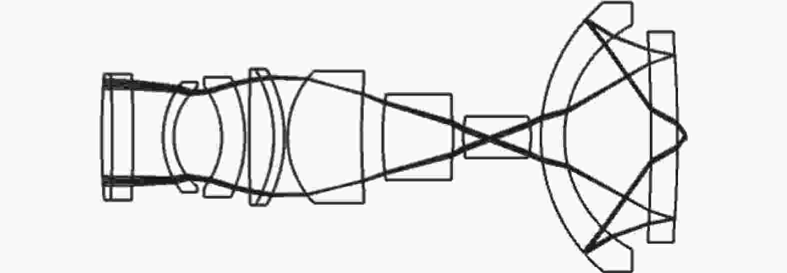
图 1 光学系统结构
Figure 1. Structure of optical system
通过查看在折反射镜面的光迹图可以确定折反射镜面具体的透射区域和反射区域,以便实际加工过程中在反射区域镀膜,尽可能让物体的光线全部进入光学系统。通过简单的计算可知,在靠近物体一侧的镜面透射区域约占该面全部面积的4.1%,在靠近像一侧的镜面透射区域约占该面全部面积的6.3%,故其余的面积可以镀反射膜。在多次反射的光学系统中,为了抑制杂散光,可以采用中心遮拦的方法对光学表面进行处理,尤其在一次成像的透镜表面,在表面喷涂特征消光图层来阻挡对成像没有贡献的光线[22]。
-
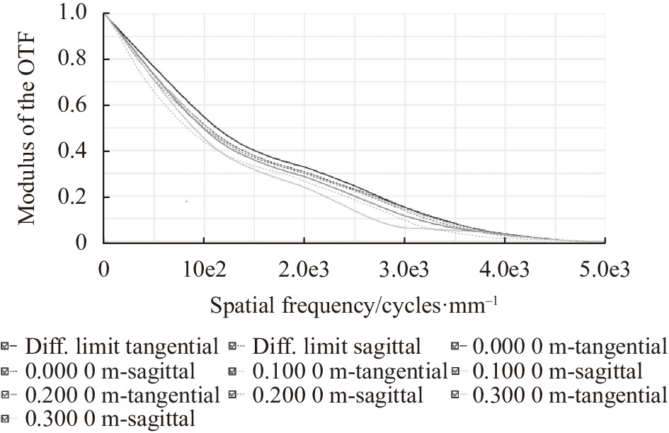
经过优化后,物镜的成像质量已满足像质要求。考虑到中心遮光部分,光学系统的像质评价曲线如图2所示。可以看出,系统全视场几乎已优化到衍射极限。

图 2 MTF曲线
Figure 2. MTF curves
图3为光学系统的轴向色差曲线,图4为色焦移曲线。可以看出,光学系统的轴向色差已得到了较好的校正,二级光谱色差大小约为0.18 μm,也已得到了较好的校正,满足系统的成像质量要求。

图 3 轴向色差曲线
Figure 3. Longitudinal aberration curves
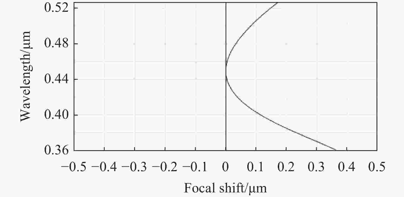
图 4 色焦移曲线
Figure 4. Focal shift curves
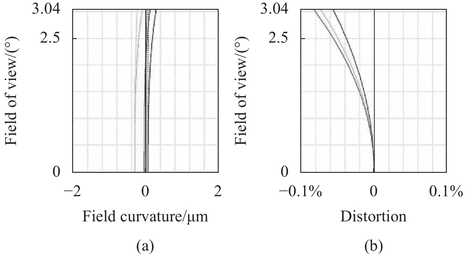
图5为光学系统场曲、畸变曲线,图6为RMS波前误差曲线,可以看出,场曲、畸变、像散均得到了较好的校正,最大畸变为520 nm波段最大视场处,仅为0.073%,且全视场波像差小于0.09λ,可认为光学系统成像质量较好,达到了设计要求。
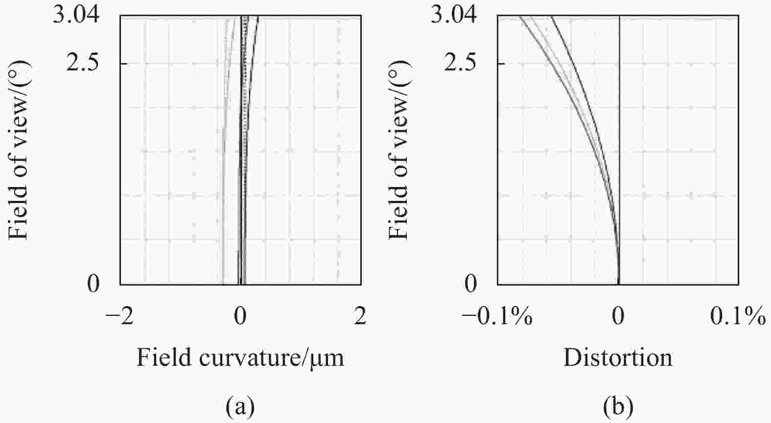
图 5 场曲、畸变曲线
Figure 5. Field curvature and distortion curves

图 6 RMS波前误差曲线
Figure 6. RMS wavefront error curve
物镜为无限远共轭,发出的平行光最大视场角小于3°,该角度可以匹配现有的大部分管透镜的视场角。考虑到与管透镜的光瞳匹配问题,在设计时光瞳预留了足够的距离适配市场上常见的管透镜,确定前后系统出入瞳位置后,以连接实现不同的放大倍率。如与200 mm标准焦距管透镜连接使用,根据公式(2)可实现约35×的放大倍率。
-
在实际生产装配过程中,由于材料自身加工的误差以及装配误差等因素,会导致光学系统成像质量下降,系统的公差要求决定着制造过程的难度和成本,故对系统进行公差分析[23]。
进行MTF公差敏感度分析,当各个表面厚度公差为±0.01 mm、各个表面的曲率半径公差为±0.01 mm、各个表面的偏心公差为±0.05 mm、各个表面的倾斜公差为±0.05°、元件表面的偏心公差为±0.05 mm、元件表面的倾斜公差为±0.05°、折射率公差为±3×10⁻⁴、阿贝数公差为0.01%时,在使用后焦补偿的情况下进行200组蒙特卡洛分析,得到的结果显示,此时较大的误差出现在两个反射面的倾斜公差,故将继续收紧折反射镜面的倾斜公差为±0.01°,在150 mm/lp程中,更应该注意折反镜组的生产和装配精度。
根据表3可以看出,仍有90%的装配情况较好,还能满足成像要求,可结合一定的方法进行实际装配[24]。根据公差分析结果可知,在实际生产装配过程中,更应该注意折反镜组的生产和装配精度。
表 3 蒙特卡洛分析结果
Table 3. Monte Carlo analysis result
Monte Carlo analysis MTF > 90% 0.61589318 > 80% 0.66301403 > 50% 0.73955057 > 20% 0.81336773 > 10% 0.87030525 -
针对半导体缺陷检测领域对光学系统的高分辨要求,文中设计了一种数值孔径为0.9、工作波段为360~520 nm的折反式物镜,仅使用11片镜片实现了高分辨的要求,较好地校正了场曲和二级光谱色差,全视场波像差小于0.09λ。利用折反射式结构压缩了光路路径,简化了光路的复杂程度。该物镜可搭配不同焦距的标准管透镜,实现不同的放大倍数,以满足检测成像的需求。该设计仅使用了球面透镜,未来该类透镜可进行进一步优化,在成本控制允许的条件内,若使用非球面透镜代替胶合透镜,可使结构更为简化。
Design of large numerical aperture and wide spectrum catadioptric objective lens (invited)
-
摘要: 为了满足半导体缺陷检测系统对成像系统高分辨的要求,依据系统的特点和设计指标,设计了一种近紫外-可见光大数值孔径折反式物镜。在近紫外-可见光波段对光学玻璃材料的色散特性进行分析,通过二级光谱理论计算,选择合适的玻璃材料,对光学系统的二级光谱进行了校正。该物镜使用11片球面透镜,结构紧凑。设计出一套光谱范围为360~520 nm、数值孔径为0.9、焦距为5.65 mm、视场大小为0.8 mm、工作距离为0.8 mm的物镜,采用无限远共轭折反式结构。设计结果表明:该物镜的MTF较好,全视场波像差小于0.09λ (λ=632.8 nm),各种几何像差均得到了较好的校正,满足复消色差条件,并且结构简单,具有较长的工作距离,为实际的生产装配和应用提供了便利。Abstract:
Objective To fulfill the stringent high-resolution prerequisites of the imaging system deployed for semiconductor defect detection, a catadioptric objective lens with a large numerical aperture, specialized for near-ultraviolet to visible light wavelengths, has been meticulously devised in accordance with the distinct characteristics and design parameters of the system. The dispersive traits of optical glass materials within the near-ultraviolet to visible light spectrum are subjected to comprehensive analysis. In order to ameliorate the secondary spectrum of the optical system, a judicious selection of appropriate glass material is undertaken based on rigorous theoretical calculations of the second-order spectrum. The constructed objective lens, comprising an assemblage of 11 spherical lenses, exhibits a compact architectural arrangement. Specifically engineered for spectral coverage spanning 360-520 nm, the objective lens boasts a numerical aperture of 0.9, a focal length of 5.65 mm, a field of view measuring 0.8 mm, and an operative distance of 0.8 mm. This innovative design embodies an infinite conjugate catadioptric configuration. The results of this design endeavor reveal a favorable Modulation Transfer Function (MTF) for the objective lens, with wave aberrations across the entire field of view quantified at less than 0.09λ (λ=632.8 nm). Furthermore, diverse geometric aberrations are effectively rectified, aligning with the stringent apochromatic prerequisites. The resultant objective lens configuration not only conforms to these demanding optical standards but also underscores simplicity in its architectural layout and an extensive operational working distance. This facilitates convenience in practical production assembly and application. Methods In the context of wide-spectrum large numerical aperture objectives, the mitigation of field curvature and secondary spectrum emerges as a focal point meriting dedicated consideration. Consequently, meticulous assessment of the field curvature and axial chromatic aberration within the system is conducted in accordance with foundational principles governing primary aberrations intrinsic to thin lens configurations. Subsequently, optimization of the objective lens ensues through a judicious amalgamation of suitable glass materials and structural arrangements, with a particular emphasis on addressing secondary spectrum intricacies. In the realm of catadioptric mirror assemblies, the formulation of the catadioptric mirror group is informed by the principles underlying the Mangin mirror. Results and Discussions Following optimization procedures, the imaging fidelity of the objective lens has satisfactorily adhered to the stipulated image quality criteria. The graphical representation illustrated in Figure 2 showcases the near-optimal alignment of the system's full field of view with the theoretical limits imposed. Evident in Figure 3, the intricate challenge of axial chromatic aberration within the optical system has been effectively ameliorated, with the secondary spectral chromatic aberration quantified at approximately 0.18 μm—this accomplishment aligns harmoniously with the prescriptive image quality prerequisites governing the system. According to Figure 4 and Figure 5, field curvature, distortion, and astigmatism are well corrected, the distortion is only 0.073% at 520 nm, and the all-encompassing wave aberration well below 0.09λ, it is judicious to assert that the optical system demonstrates commendable imaging fidelity. The objective lens, embracing an infinity-conjugate configuration, accommodates a maximal angular field of view for emitted parallel light of approximately 3°. To cater to various magnification needs, a tube lens, appropriately matched in parameters, can be affixed posteriorly to the objective lens. For instance, coupling the objective lens with a standard tube lens possessing a focal length of 200 mm, as delineated by the formula (2), facilitates the realization of a magnification factor of 35×. Conclusions In response to the high-resolution demands inherent to optical systems within the domain of semiconductor defect detection, this paper introduces a catadioptric objective lens featuring a numerical aperture of 0.9 and an operational wavelength range spanning 360 nm to 520 nm. With a remarkably streamlined configuration composed of just 11 lenses, the lens design effectively meets the stringent criteria for high-resolution output. By effectively addressing challenges related to field curvature and secondary spectral chromatic aberration, the lens achieves comprehensive correction. Wave aberration analysis demonstrates that the entire field of view remains well below 0.09λ. The integration of a catadioptric structure serves to condense the optical path while concurrently simplifying its intricacy. Notably, the designed objective lens can be seamlessly paired with commercially available standard tube lenses of varying focal lengths, thereby offering the flexibility to attain diverse magnification levels as required for inspection imaging purposes. -
表 1 物镜设计指标
Table 1. Objective design specifications
Parameter Specification Spectral range/nm 360-520 FOV/mm ≥0.5 NA 0.9 Working distance/mm ≥0.6 Focal length ≤10 Total length/mm ≤60  下载: 导出CSV
表 2 玻璃色散特性
Table 2. Characteristics of glass dispersion
Materials P V F_SILICA 0.37012987 30.23 CaF2 0.36792453 41.39 H-K9 LAGT 0.36363636 28.09 5742 0.34375000 16.80 5859 0.36363636 26.01 P-SK60 0.37718924 26.56 I-FSL5Y 0.36708861 31.32 K10 0.35680751 23.99 S-FSL5 0.36708861 31.32 N-PK52A-2 0.36879433 35.71 F5 0.33653846 14.92
下载: 导出CSV
表 3 蒙特卡洛分析结果
Table 3. Monte Carlo analysis result
Monte Carlo analysis MTF > 90% 0.61589318 > 80% 0.66301403 > 50% 0.73955057 > 20% 0.81336773 > 10% 0.87030525
下载: 导出CSV
-
[1] 苏朋. 365 nm光刻照明系统中变焦系统的设计及公差分析[J]. 红外与激光工程, 2022, 51(7): 20210524. doi: 10.3788/IRLA20210524. Su Peng. Design and tolerance analysis of the zoom system in 365 nm UV lithography illumination system [J]. Infrared and Laser Engineering, 2022, 51(7): 20210524. (in Chinese) doi: 10.3788/IRLA20210524 [2] Armstrong J J, Chuang Y, Shafer D R. Catadioptric imaging system employing immersion liquid for use in broad band microscopy: US, 20080247035A1 [P]. 2008-10-09. [3] Shafer D, Chuang Y, Armstrong J. High performance catadioptric imaging system: US, 20040165257A1 [P]. 2004-08-26. [4] 薛金来, 巩岩, 李佃蒙. N. A. 0.75平场复消色差显微物镜光学设计[J]. 中国光学, 2015, 8(06): 957-963. doi: 10.3788/CO.20150806.0957. Xue Jinlai, Gong Yan, Li Dianmeng. Optical design of the N. A. 0.75 plan-apochromatic microscope objective [J]. Chinese Optics, 2015, 8(6): 957-963. (in Chinese) doi: 10.3788/CO.20150806.0957 [5] 张新, 管海军, 王超, 等. 宽谱段大数值孔径的显微物镜: 中国, 201911335716.6[P]. 2019-12-23. [6] 黄木旺, 刘旭, 林法官. 大视场大数值孔径显微物镜光学设计[J]. 激光与光电子学进展, 2023, 60(5): 0518001. doi: 10.3788/LOP220458. Huang Muwang, Liu Xu, Lin Faguan. Design of large field of view and high numerical aperture microscope objective [J]. Laser & Optoelectronics Progress, 2023, 60(5): 0518001. (in Chinese) doi: 10.3788/LOP220458 [7] Williamson D M. Broadband catadioptric microscope objective with small central obscuration: US, 201615762423[P]. 2018-11-27. [8] Graeupner P, Kuerz P, Stammler T, et al. EUV optics: status, outlook and future [C]// Proceedings of SPIE, 2022, 12051: 1205102. [9] Yan X, Li Y Q, Li Y H, et al. Design of an extreme ultraviolet lithography projection objective with a grouping design method through forward and reverse real ray tracing [J]. Applied Optics, 2022, 61(25): 7449-7454. doi: 10.1364/AO.469274 [10] 崔志英, 王赟, 赵宇, 等. 一种20倍大数值孔径平场复消色差显微物镜: 中国, 202111524464.9[P]. 2023-09-01. [11] 王风超. 一种大视场, 长工作距的复消色差显微物镜: 中国, 202111104489.3[P]. 2023-09-01. [12] Mao Shanshan, Li Yanqiu, Liu Ke, et al. Optical design of high numerical aperture extreme ultraviolet lithography objective with freeform surfaces [J]. Infrared and Laser Engineering, 2019, 48(8): 0814002. doi: 10.3788/IRLA201948.0814002 [13] 周恩源, 刘丽辉, 刘岩, 等. 近红外大数值孔径平场显微物镜设计[J]. 红外与激光工程, 2017, 46(07): 188-194. doi: 10.3788/IRLA201746.0718006. Zhou Enyuan, Liu Lihui, Liu Yan, et al. Design of high NA flat-field microscope objective for near infrared [J]. Infrared and Laser Engineering, 2017, 46(7): 0718006. (in Chinese) doi: 10.3788/IRLA201746.0718006 [14] Matsuyama T, Ohmura Y, Fujishima Y, et al. Catadioptric projection lens for 1.3 NA scanner [C]//Optical Microlithography XX, Proceedings of SPIE, 2007, 6520: 652021. [15] 郁道银, 谈恒英. 工程光学[M]. 第3版. 北京: 机械工业出版社, 2011. [16] 郁晓晖. 宽光谱大数值孔径平场复消色差物镜设计[D]. 南京: 南京理工大学, 2018. [17] Kneer B, Flagello D G, Gräupner P, et al. Catadioptric lens design: the breakthrough to hyper-NA optics [C]//Proceedings of SPIE, 2006, 6154: 615420. [18] 黄翌敏, 龚海梅. 一种用于紫外探测器的大相对孔径宽波段紫外物镜: 中国, 100406951C[P]. 2008-07-30. [19] Li X, Wu M. Design of Compact space optical system with large relative aperture and large field of view based on mangin mirror [C]//6th International Symposium of Space Optical Instruments and Applications, 2021: 253-265. [20] 任志广, 李旭阳, 倪栋伟. 大相对孔径、大视场、紧凑型空间光学系统设计[J]. 光学学报, 2019, 39(9): 0922001. doi: 10.3788/AOS201939.0922001. Ren Zhiguang, Li Xuyang, Ni Dongwei. Compact space optical system design with large relative aperture and field of view [J]. Acta Optica Sinica, 2019, 39(9): 0922001. (in Chinese) doi: 10.3788/AOS201939.0922001 [21] 李景镇. 光学手册[M]. 西安: 陕西科学技术出版社, 2010. [22] 王虎, 陈钦芳, 马占鹏, 等. 杂散光抑制与评估技术发展与展望(特邀)[J]. 光子学报, 2022, 51(7): 0751406. doi: 10.3788/gzxb20225107.0751406. Wang Hu, Chen Qinfang, Ma Zhanpeng, et al. Development and prospect of stray light suppression and evaluation technology (Invited) [J]. Acta Photonica Sinica, 2022, 51(7): 0751406. (in Chinese) doi: 10.3788/gzxb20225107.0751406 [23] Xu Weicai. Optical design and imaging performance compensation for the lithographic lens [D]. Changchun: Chinese Academy of Sciences (Changchun Institute of Optics, Fine Mechanics and Physics, Chinese Academy of Sciences), 2011. (in Chinese) [24] 杜国军, 王春雨, 欧宗耀等. 多基准轴透射式系统装调方法[J]. 应用光学, 2021, 42(02): 247-254. doi: 10.5768/JAO202142.0201007. Du Guojun, Wang Chunyu, Ou Zongyao, et al. Assembly and adjustment method of multi-reference axis transmission optical system [J]. Journal of Applied Optics, 2021, 42(2): 247-254. (in Chinese) doi: 10.5768/JAO202142.0201007 -

 点击查看大图

图(6) / 表(3)
计量
- 文章访问数: 100
- HTML全文浏览量: 17
- PDF下载量: 48
- 被引次数: 0

