


-
金刚石是一种独特的材料,能在多种极端环境满足应用要求,如表1所示。它在室温下具有极高的导热系数、硬度[1]、声波速度和载流子迁移率[2]。金刚石在可见光谱范围内表现出高度的透明性,使其能被广泛应用于光学窗口[3]。同时,它还是优良的绝缘体,在进行硼元素掺杂后也可以作为高质量的p型半导体。此外,它还具有独特的辐照稳定性、化学惰性、生物相容性和许多其他重要特性,这决定了金刚石材料的诸多应用。
金刚石集多种优秀的性能于一身,使其成为世界上最理想的材料之一,但同时它也被称之为“最难加工”的材料,因为目前传统工艺下不存在能够同时满足加工精度和加工效率的有效加工方法。随着近年来化学气相沉积(Chemical Vapor Deposition, CVD)技术的快速发展,在推动人工培育钻石成本的迅速降低,促进CVD金刚石的广泛应用的同时,也对金刚石的精细加工也提出了迫切需求。
表 1 金刚石的性质和应用
Table 1. Properties and applications of diamond
Property Value Application Bandgap/eV 5.4 High-temperature electronics Carrier mobility/(cm2·V−1·s−1) Holes 3 800; electrons 4 500 Radiation-hard detectors Optoelectronic switches Resistivity/Ω·cm 1013-1015 Thermal conductivity
/(W·m−1·K−1)2 000-2 400 Heat sinks Dielectric constant 5.7 Optical transmission range 225 nm- radio frequency Photonics and MW devices Hardness/GPa (81±18) Tools, surgery blades Acoustic wave velocity/(km·s−1) 18.4 along <100> Surface acoustic wave devices Thermal expansion coefficient
/(10−6 ·K−1)0.8(293 K) Photonics and MW devices Corrosion resistance Stable in HF Electrochemistry Negative electron affinity Electron emitters Biocompatibility Biomedicine 针对金刚石的加工,目前研究人员已经应用了多种加工方法,包括电火花加工[4],磨料水射流加工[5-6],机械加工[7-8]以及激光加工[9]等。在这些方法中,激光加工加工成本低,可重复性好,是一种高效可控的加工金刚石的方法[10]。早在20世纪60年代初就有关于激光加工金刚石的报道。目前在金刚石材料的激光加工研究中,主要用到的激光类型如表2所示。其脉冲频率大多在0.1 Hz~100 kHz之间,最短的脉宽为飞秒尺度。在实际加工过程中通过选择合适的激光波长、脉宽和功率等参数可以进行金刚石的高质量及特殊形状加工,其加工精度可以达到微米级别甚至纳米尺度[11−13]。
表 2 用于金刚石加工的激光种类
Table 2. Types of laser used in diamond processing
Type Nd:YAG Ti:Al2O3 Cu Ar+ KrF ArF CO2 Wavelength/nm 1 064 532 800 510.5 488 248 193 10 600 Energy/eV 1.17 2.33 1.55 2.42 2.54 5.0 6.42 0.12 Mode Pulse/continuous Pulse Pulse Continuous Pulse Pulse Pulse 针对金刚石难加工、难成型的特点,结合激光先进加工技术,文中综述了金刚石激光加工机理,对比不同类型的激光加工效果,同时对激光在金刚石切割、打孔、微槽道成型、激光平整化、激光剥离等方面的应用研究进行总结,介绍了新型的激光加工技术,对金刚石激光加工技术未来的研究方向提出了设想。
-
金刚石在激光加工过程中发生的升华或化学刻蚀均不是直接发生的,而是首先要经历金刚石向石墨相的转变过程,这种碳相的转变是金刚石激光加工过程中的关键点之一,金刚石材料的石墨化行为降低了其加工难度[14]。
-
1917年,基于量子理论爱因斯坦提出了一个崭新的概念:在物质与辐射场的相互作用中,构成物质的原子或分子可以在光子的激励下产生光子的受激发射或吸收[15],这为后续激光器的出现奠定了基础。当外来光子的频率满足能级跃迁要求,就会使原子中处于高能级的电子在外来光子的激发下向低能级跃迁,并释放与入射光子频率、传播方向、相位及偏振均相同的受激辐射光子[16]。Nd:YAG晶体是典型的激光晶体,其结构能级简图如图1所示。
受激辐射光放大、集居数反转以及满足激光振荡的临界状态是激光产生的三大条件[17],而这对应了激光器泵浦源、激光工作介质和谐振腔三个基本组成结构。基于上述激光产生原理,激光是一种受激辐射相干光源,具有高亮度、高方向性、高单色性和高相干性的特点,具有极好的时间和空间控制性能。
-
激光烧蚀(又称激光加工)是通过激光束照射固体表面从而去除表面材料的过程。在低激光通量下,材料吸收激光能量而加热并蒸发(或升华)。影响激光与固体材料相互作用的因素较多,包括脉冲长度、波长、激光功率、重复频率、光束特征以及固体材料的物理性质等。在固体内部,光可发生透射、反射和吸收,只有吸收的能量才能在固体内部产生烧蚀作用,而反射和透射光影响烧蚀区域预热体积的形状及位置。激光能量在固体材料中的吸收受材料吸收系数影响,短脉冲和超短脉冲激光辐照在金刚石材料中的吸收特征存在巨大差异,见图2。对于无杂质的单晶金刚石而言,仅对光子能量超过能带间隙(5.4 eV)存在有效吸收(对应波长为229 nm[19])。然而,在实际的加工过程中,常使用532 nm(绿光)和1064 nm(近红外)激光进行加工,在理想情况下,这些波长的激光并不能被无杂质的金刚石吸收,而金刚石的能带结构受其本征和非本征缺陷的强烈影响,包括晶界、晶体缺陷、非金刚石相以及掺杂原子等[20]。这些缺陷还会使金刚石的激光烧蚀阈值(ablation threshold)降低,高浓度的缺陷对应于低的烧蚀阈值,这有利于激光加工。
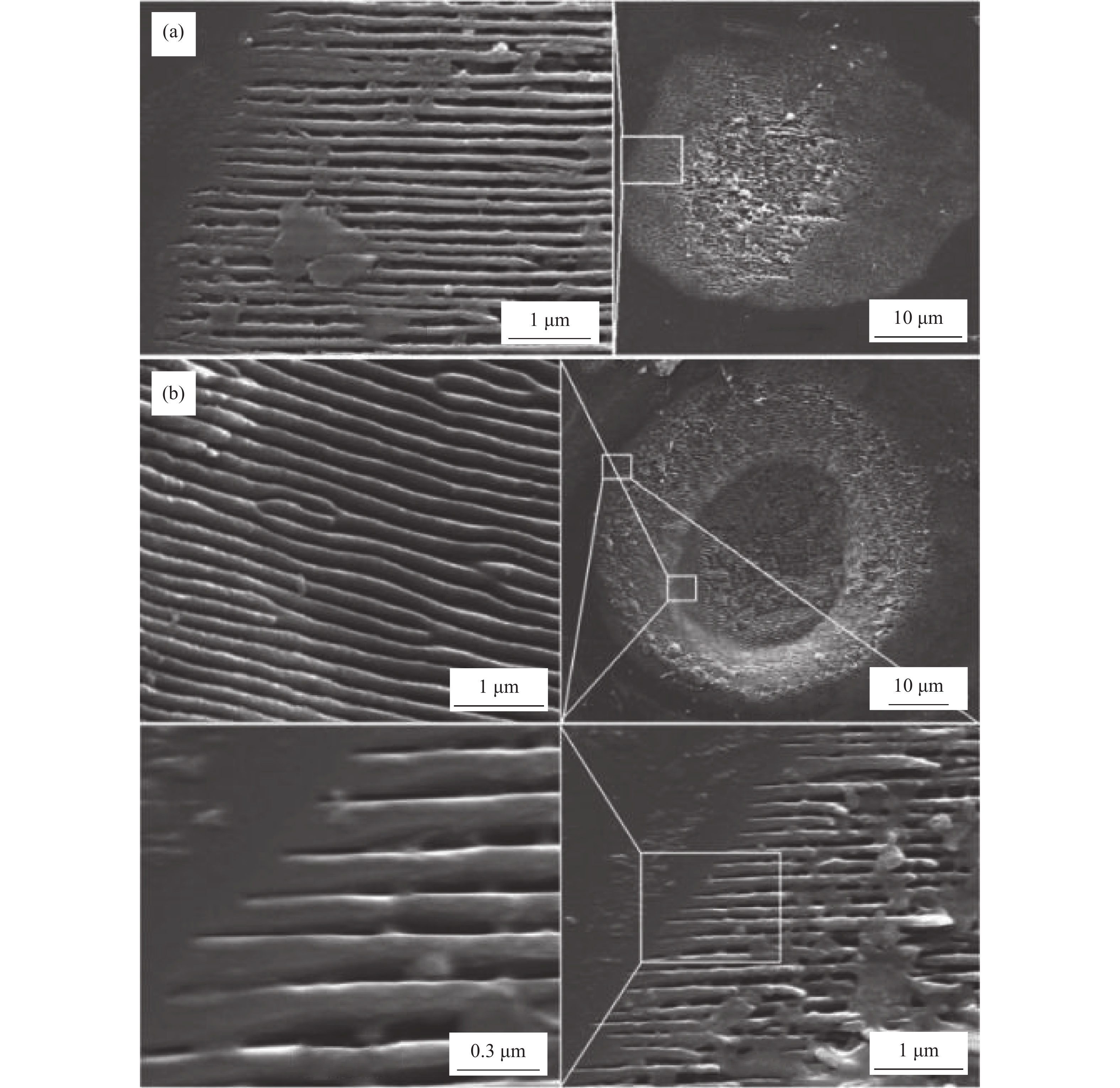
而对于超短脉冲激光辐照过程中发生的多光子吸收情况而言,电子可以吸收多个光子从而被激发,此过程要求聚焦光束有高的时间光子密度和空间光子密度[22]。因束缚电子的电离势远大于激光单光子的能量,所以一般情况下不会释放束缚电子,在激光强度高于1012 W/cm2时可以产生多光子电离,多光子电离可以释放束缚电子,电子可以同时吸收多个光子的能量产生激发电子,激发电子与声子的耦合导致晶格加热,从而发生相爆炸[23]。湖南大学熊彪[24]等于2019年有过飞秒激光加工单晶金刚石锥形阵列的报道,如图3所示,尽管金刚石对实验使用的波长为1030 nm激光有较好的透过性,但仍能通过多光子电离和缺陷增强等实现对高峰值功率的吸收。

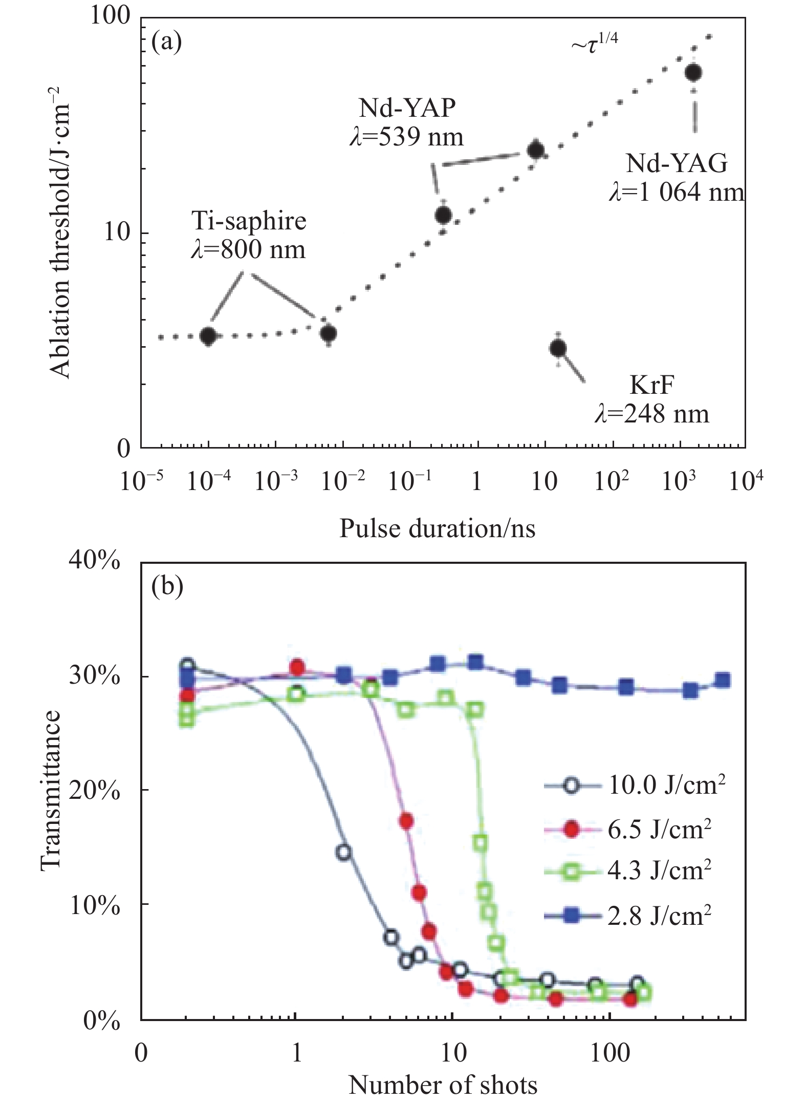
烧蚀阈值还会随着脉冲宽度和脉冲数变化,M.S. Komlenok[25]对其进行了总结,如图4所示。通常而言,更短的脉冲持续时间总会对应着更小的烧蚀阈值。在激光加工过程中通常采用多个脉冲降低烧蚀表面区域处的烧蚀阈值,在长时间的多脉冲激光照射下,多脉冲的累积作用使得材料的光吸收系数逐渐增大,直到一次激光脉冲吸收的能量就足以将该类石墨状缺陷的晶格键破坏,进而产生烧蚀效果[26]。同时,要使金刚石在低能量密度的激光照射下出现石墨化,需要增大脉冲数量,且单道脉冲能量越低,所需要的脉冲数量越多。基于此,当前金刚石激光加工向着短波长、窄脉冲持续时间的方向努力发展。
-
金刚石是共价晶体,其一个s轨道和三个p轨道杂化形成四个能量相等且按正四面体排列的sp3杂化轨道,使电子承受最小的排斥力。在短脉冲激光照射下,金刚石温度急剧升高,使得C-C共价键断键重连,每个碳原子四个外层价电子中的三个2s,2px,2py以sp2杂化轨道形式在同一平面内通过σ键与三个碳原子形成共价单键,各轨道中心轴间成120°夹角。另一个未参与杂化的2 pz轨道电子与此平面垂直,在pπ轨道上形成不饱和的π键[27],即发生了金刚石石墨化转变。
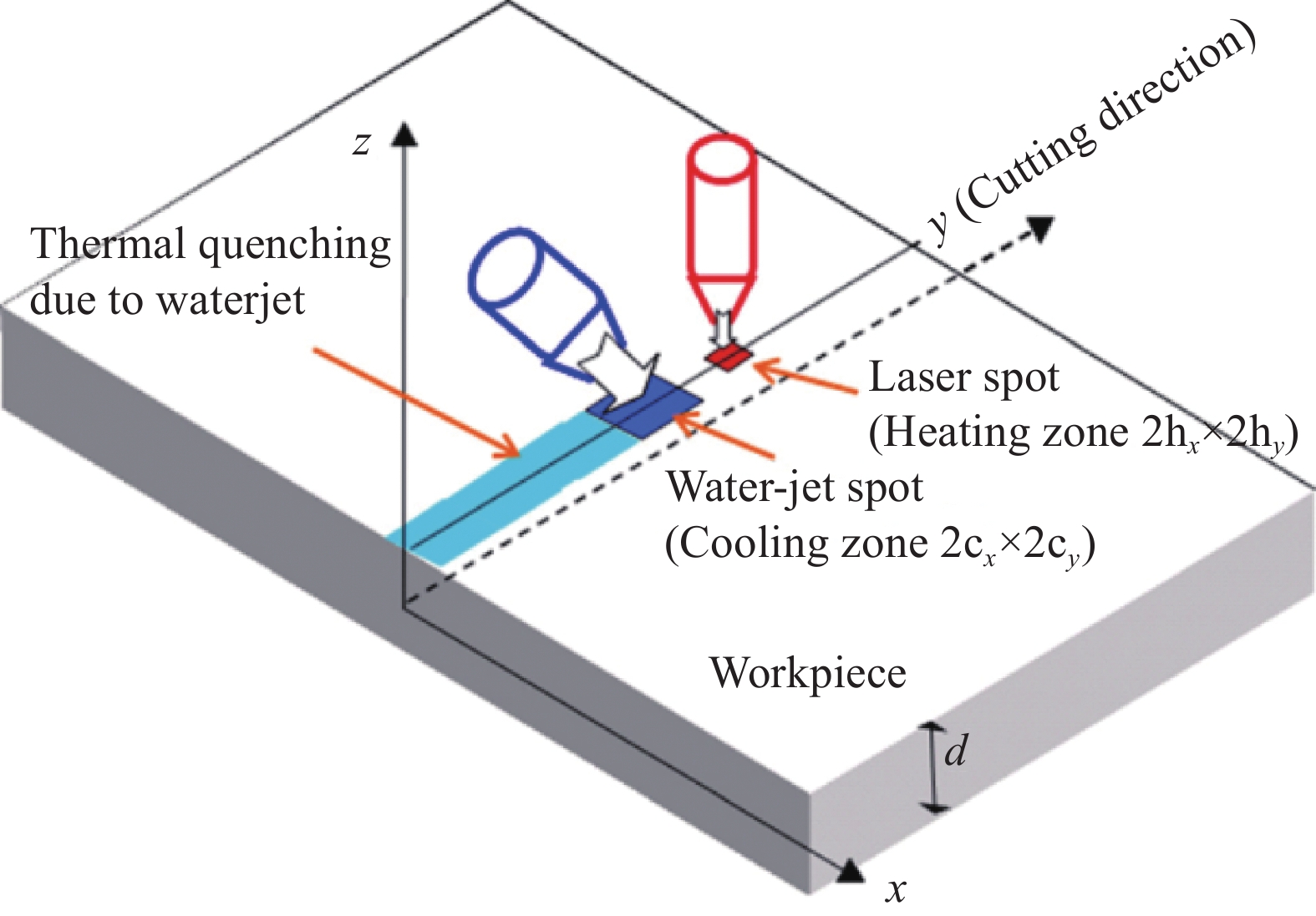
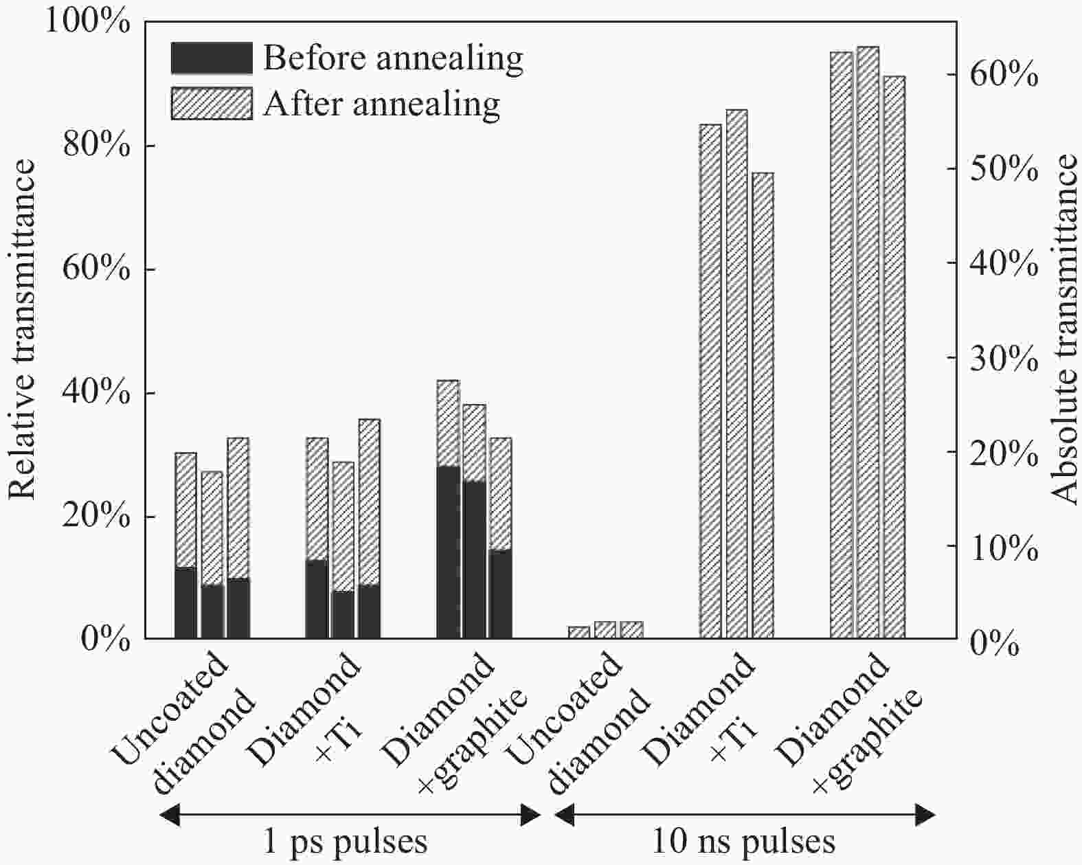
激光加工金刚石时往往会引起金刚石透过率的降低,这种情况在使用长波长激光加工时更为明显。激光造成的内部损伤是造成此种情况的主要原因,不同脉冲持续时间的激光均能引起金刚石表面的光击穿。John Smedley[28]等在使用266 nm的皮秒激光器对多晶金刚石进行加工时能明显观察到内部存在不透明缺陷,且在长脉冲宽度(10 ns)以及波长(532 nm)条件下,多晶金刚石中激光诱导缺陷的尺寸和数量增加。T.V. Kononenko[29]等对近红外皮秒激光(1030 nm;1 ps)加工多晶金刚石进行研究,认为在金刚石表面石墨化和烧蚀开始之前,在金刚石的亚表层位置会发生单次或者多次的光击穿,每次的击穿效应均会产生微米级别的石墨包裹体[30]。在此基础上,他们提出了在加工之前预先于表面镀制吸收层(Ti或者石墨)以减少亚表面光击穿的方法(如图5所示),发现对于脉冲持续时间较长(10 ns)的激光加工过程而言,吸收层的存在能有效避免金刚石内部加工损伤的出现,而对于短脉冲持续时间的激光加工过程则没有明显的效果。
金刚石的光电性质,包括光吸收和光子对电子的量子效率,在很大程度上取决于其固有的晶体结构和杂质的存在。无杂质的纯金刚石晶体中的光电流可由紫外光辐照下的光子吸收引起,但由于实际金刚石内部杂质和缺陷的存在使得可见光也能造成光子吸收。这表明金刚石内存在的缺陷能引起低能光吸收效应,从而增加材料的光电导。
激光与金刚石作用会带来NV色心(Nitrogen- Vacancy color center, NV center)的改变,近年来,利用超快激光诱导产生色心受到了越来越多的关注。华东师范大学Yan Liu[32]等利用高能飞秒激光辐照高氮含量的人造金刚石,并在激光辐照位置探测到了NV色心的产生。Vitali V. Kononenko[33]等人于2017年提出了表面纳米烧蚀制备NV色心的概念,其通过飞秒激光照射金刚石表面从而实现NV色心的有效可控产生,如图6所示。飞秒激光诱导的单NV色心与波导等光学元件进行集成应用的相关工作也是目前激光加工研究的重要方向。
-
激光加工金刚石时,由于入射激光束的形状、强度及偏振不同造成加工表面形貌的差异。当激光以较低能量密度入射时会立即在热影响区内出现sp2石墨化现象,而在激光密度较高的入射激光作用下,根据入射激光束的脉宽该区域会迅速升华[34]。金刚石在线偏振激光辐照作用下,表面会产生周期性的表面结构,Magdalena Forster[35]等使用飞秒激光(800 nm;60 fs)加工氮掺杂的Ib型金刚石,在垂直于电场极化方向的高空间频率激光诱导下,形成了周期为50 nm和200 nm的周期性表面结构。其中50 nm的周期性结构来自金刚石的石墨化转变,而200 nm周期性结构仍由晶态金刚石组成。需要指出的是:激光加工金刚石表面产生的周期性结构比入射激光波长小得多,相较于脉冲持续时间更长的纳秒和皮秒激光而言,飞秒激光产生的周期性特征更小从而更适合用于纳米光栅的加工。激光能量密度和脉冲数量也会对产生的纳米周期性结构产生影响,图7是线偏振飞秒激光(800 nm;125 fs)在接近金刚石烧蚀阈值(1.9 J/cm2)的激光能量密度以及脉冲数为3000下照射金刚石样品的表面形貌,在加工区域的边缘存在规则的170 nm的周期性纳米尺度光栅,当脉冲数量为8000激光能量密度为2.8 J/cm2时加工区域处的周期性结构增大至190 nm[36]。2021年,Mastellone[37]等利用延时交叉偏振飞秒激光脉冲序列在金刚石表面获得了两个超高频结构周期(Λ≈λ/10≈80 nm)的微纳结构,并探究了该结构的形成机理,如图8所示。

图 7 800 nm飞秒激光辐照金刚石表面扫描电镜图片。(a)于3000脉冲激光能量密度1.9 J/cm2形成的170 nm周期性结构;(b)于8000脉冲激光能量密度2.8 J/cm2形成的190 nm周期性结构[36]
Figure 7. Scanning electron microscope images of diamond surface irradiated by 800 nm femtosecond laser. (a) 170 nm periodic structure formed at 3000 pulse laser energy density of 1.9 J/cm2; (b) 190 nm periodic structure formed at 8000 pulse laser energy density of 2.8 J/cm2 [36]
-
激光加工可以结合计算机数控系统、先进的光学系统以及高精度和自动化的工件定位,从而形成研制和生产加工中心[38]。将激光加工技术应用于金刚石加工,可实现金刚石的高效、高精度加工。不同激光束类型作用于金刚石表面达到的加工效果存在巨大差异。
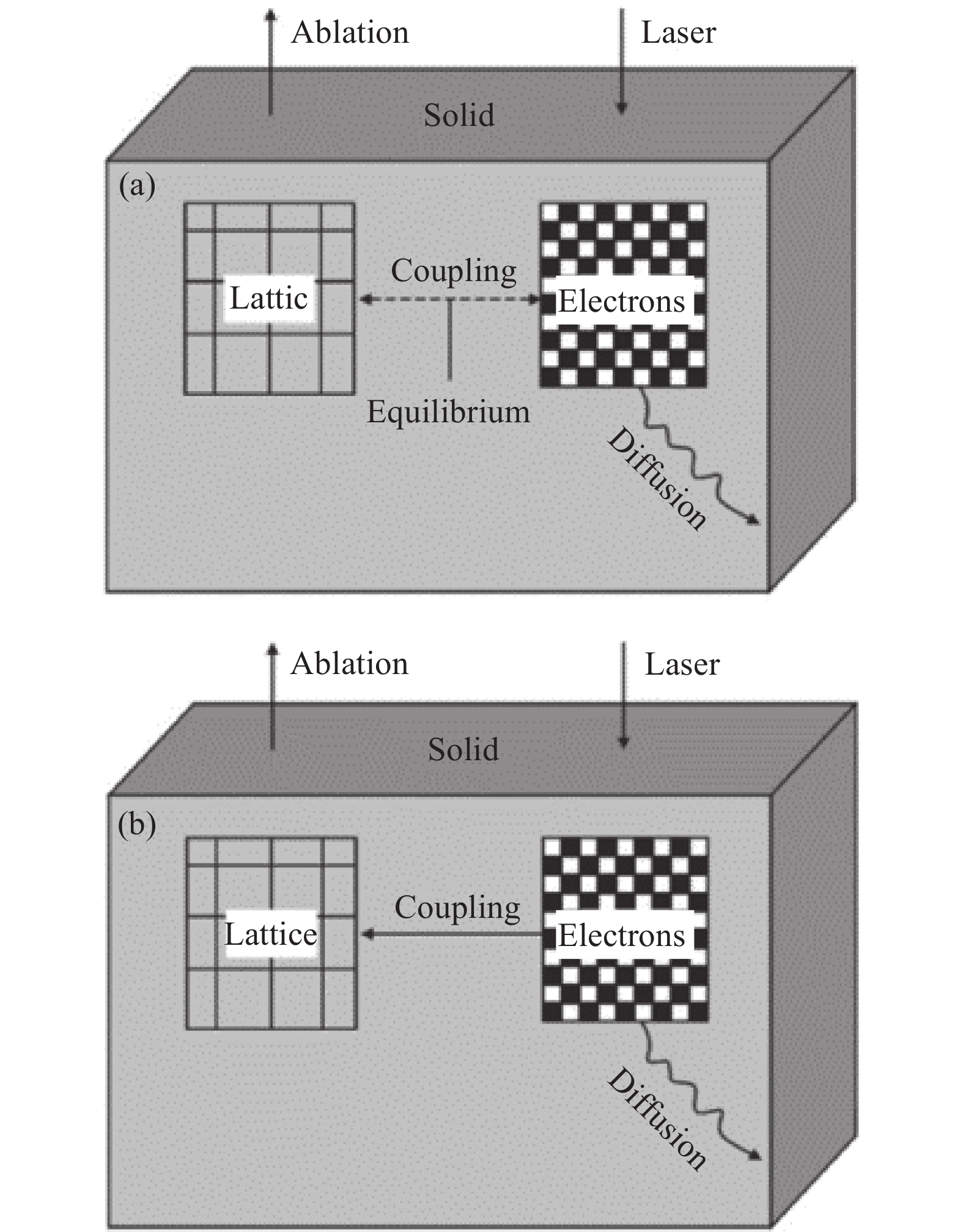
用于金刚石加工的激光可依据激光脉冲长度和原子晶格碰撞之间的大小关系分为“热加工”和“冷加工”两类[39],最具代表性的为纳秒激光和飞秒激光,两种典型激光与电子、晶格的相互作用模型如图9所示。对于金刚石而言,其电子和空穴的弛豫时间分别为1.5 ps和1.4 ps[40],激光与金刚石作用时电子和晶格之间发生热传递,对于脉冲持续时间较长的纳秒激光而言,其电子中沉积的激光能量在激光脉冲照射材料的时间内就传给晶格,从而引起材料的加热并达到热平衡状态,见图9(a),该过程中存在明显的热效应,故称其为“热加工”;而对于飞秒激光而言,其激光脉冲宽度小于电子声子相互作用的时间尺度,电子中沉积的激光能量来不及传给离子,激光脉冲辐照就已经结束。此时离子的温度比较低,故将其称为“冷加工”,见图9(b)。
-
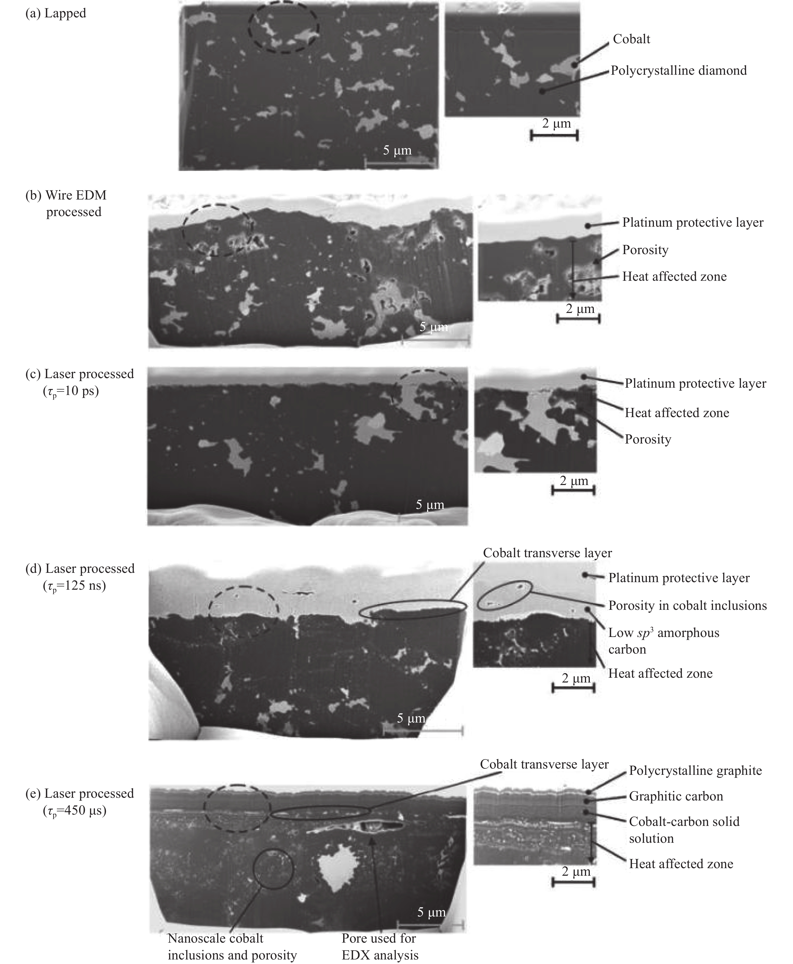
微秒激光的脉宽较宽,通常适用于粗加工,在锁模技术出现之前,激光脉冲大多在微秒与纳秒量级,当前关于微秒激光直接加工金刚石的报道较少且大多关注后端的加工应用领域。笔者课题组使用波长为1064 nm的Nd:YAG型微秒精密激光切割机完成了金刚石微槽道,冷板等金刚石热沉结构的加工并多次在学术期刊上有过发表[9, 41-42]。长脉宽的微秒激光在加工时伴随着较为强烈的热损伤,Gregory Eberlea[43]等将微秒激光加工得到的聚晶金刚石(poly-crystalline diamond, PCD)复合材料与其它加工方法得到的结果进行了表征对比,如图10所示。从图10(e)中可以看出当使用微秒激光进行加工时,PCD复合材料中存在明显的热交换,与纳秒激光不同,微秒激光的峰值功率在几千瓦且脉冲持续时间长,导致存在较深的热影响区,如图热影响区达到6.8 μm。

图 10 不同加工方式得到PCD复合材料的聚焦离子束(Focused ions beam, FIB)截面图。(a)研磨;(b)电火花加工;(c)脉宽10 ps激光;(d) 脉宽125 ns激光;(e) 脉宽450 μs激光
Figure 10. FIB cross sections of PCD composites obtained by: (a) Lapping; (b) Wire EDM; (c) Laser when pulse width =10 ps; (d) Laser when pulse width =125 ns; (e) Laser when pulse width =450 μs
-
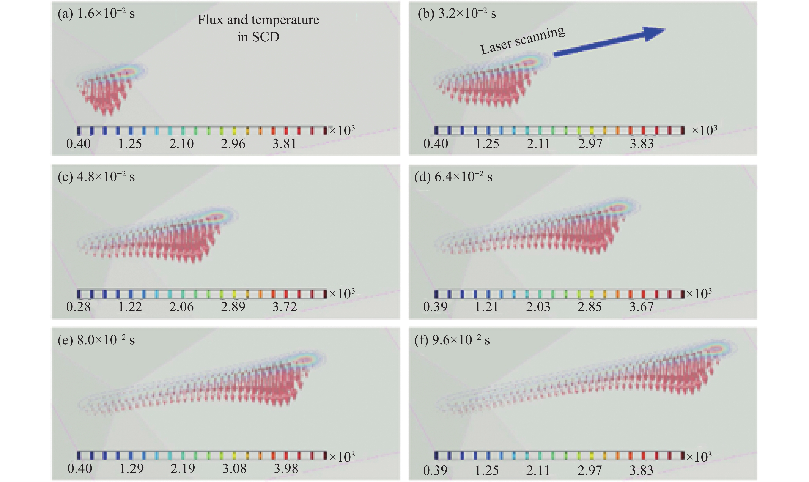
目前纳秒激光占据了较大的市场分额,同时其具有稳定性好,成本低,加工时间短等优点,在企业生产中广泛应用[44]。通常而言,纳秒激光烧蚀过程对样品具有热破坏性,宏观上表现为加工产生较大的热影响区。南京航空航天大学Zhen Zhang[45]等人建立了三维移动纳秒脉冲高斯激光烧蚀单晶金刚石的有限元模拟模型,并得到了不同扫描时间下单晶金刚石内热传导及温度分布,如图11所示,该模型与实际结果有较好的匹配关系,模型具有良好的预测能力。

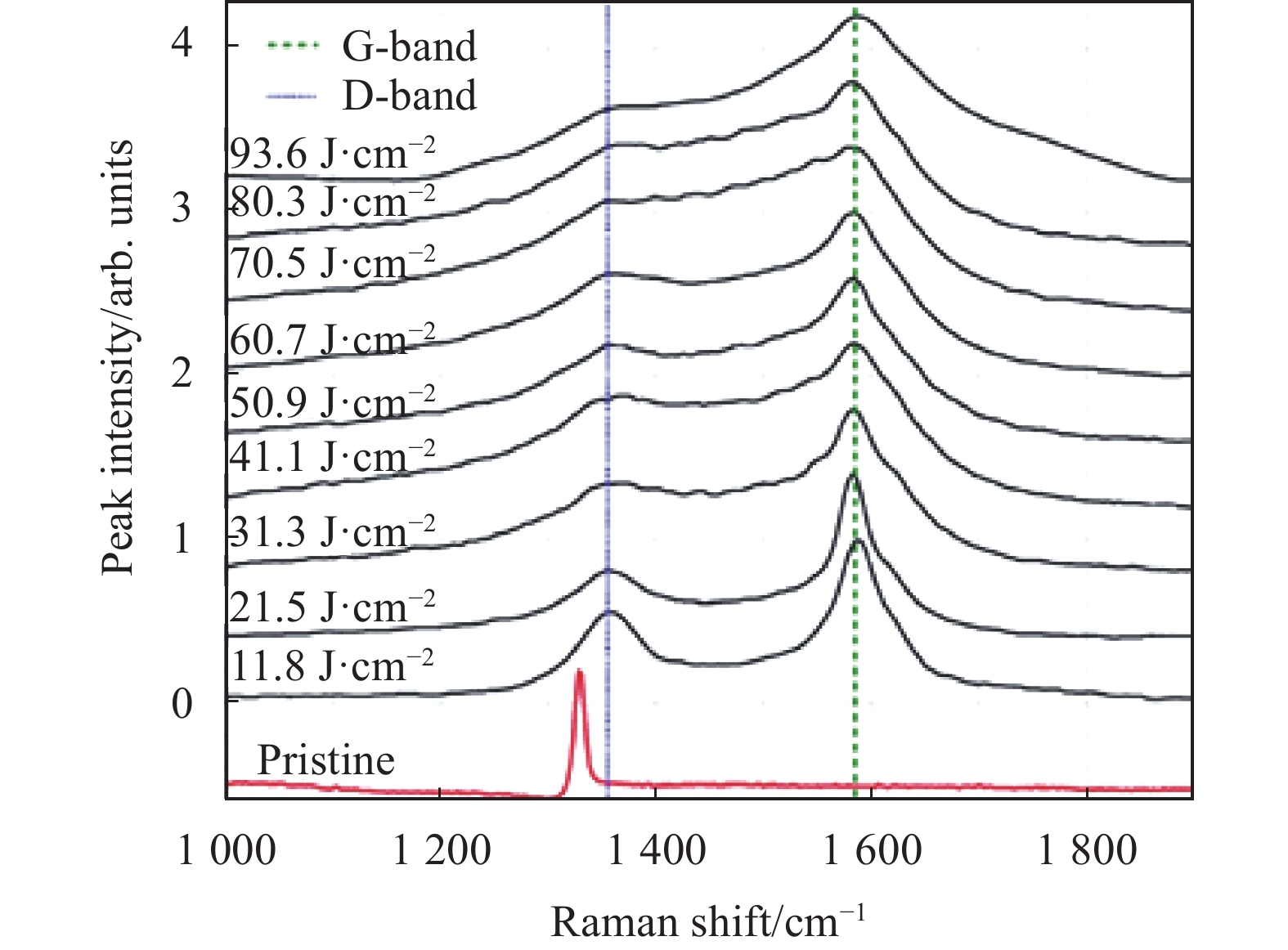
日本庆应义塾大学Nozomi Takayama[46]将纳秒激光加工(激光参数为脉宽15.6 ns;频率1 kHz;波长532 nm;光斑直径85 μm;最大输出功率Pavg>1 W)金刚石产生的缺陷分成四类(开裂、波纹、变形槽道以及碎屑沉积),同时对各种缺陷的产生原因进行了解释。裂纹是因为加工过程中急速的温度变化引起;由于凹槽壁反射激光产生干涉而形成波纹;凹槽的变形及其与高斯激光的偏差是由于激光诱导等离子体增强吸收导致;而沉积的碎屑主要有两种类型:圆形的石墨碳颗粒和较小的不规则金刚石颗粒。G.B.J. Cadot[47]等研究了不同激光通量加工后的金刚石拉曼光谱,见图12,在较低的激光通量下,拉曼光谱存在1380 cm−1以及1580 cm−1两个特征峰,表明低激光通量产生的石墨为大团簇形状,对晶体结构的干扰较小,随着激光通量的增加,代表无序石墨结构的D峰以及石墨G峰均宽化这表明晶格中缺陷数量随之增加。

图 12 不同激光通量下加工凹坑处的Raman光谱图像
Figure 12. Raman spectral images of machined pits under different laser fluxes
T.V. Kononenko[48]等研究了辐照条件(脉冲持续时间、波长、激光强度和脉冲数)对激光诱导石墨化层结构和厚度的影响,对于纳秒激光而言,脉冲宽度的减小将会导致石墨化层厚度的显著减少。纳秒激光切割金刚石时表面存在大量碎屑[10],这些碎屑由具有不同结晶度的复杂石墨单元组成,且从表面到切缝中心分别为高取向石墨,波纹状石墨以及纳米晶体石墨。这进一步证明了金刚石加工过程中材料的去除机制是石墨化和随后石墨化层的升华。
-
皮秒激光加工既不同于纳秒激光的热平衡烧蚀,也不完全等于飞秒激光的冷加工,脉冲持续时间的显著减小极大程度地降低了热影响区带来的损伤。温邱玲[49]等人使用红外皮秒激光(1064 nm,15 ps)加工CVD单晶金刚石微槽,发现仅在微槽的边缘存在不规则微小崩边和微裂纹,同时其激光烧蚀金刚石温度场仿真结果也表明激光辐照能量主要分布在金刚石的表面,以热传导方式进入金刚石内部的激光能量极少,这样产生的热影响区也是极小的。Nozomi Takayama[50]等利用皮秒脉冲激光(1030 nm,800 ps)加工具有特殊结构的单晶金刚石刀具,当激光参数为:激光通量15.3 J/cm2,重复频率100 kHz,可以快速加工出无任何边缘开裂的刀具。与纳秒激光类似,皮秒激光与金刚石相互作用时也是通过表面石墨化进行,并且对加工后的金刚石微槽底部进行拉曼分析,如图13所示,结果表明:随着皮秒激光能量密度的增加,石墨峰出现了明显的红移[49]。
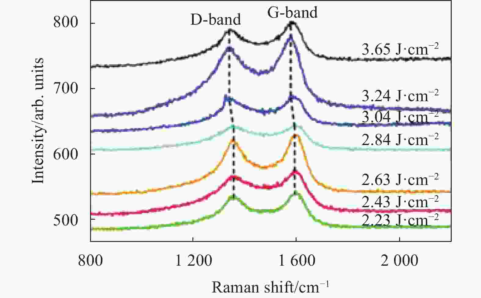
图 13 不同激光能量下皮秒激光烧蚀金刚石微槽中心位置处的拉曼光谱
Figure 13. Raman spectra of picosecond laser ablation of diamond micro-grooves at different laser energies
Sergei M. Pimenov[51−53]等利用皮秒激光作用于金刚石内部,观察到金刚石内部产生石墨化现象,如图14所示,并基于此制备了石墨化的微结构阵列,并研究了晶体取向对皮秒激光烧蚀过程的影响。同时,他们在石墨化位置处发现了3 H色心(一种自间隙相关的色心)、NV色心的产生,且NV色心的荧光由于激光体修饰过程有增强的现象。
-
1981年,R. L. Fork[54]等人报道了第一台脉冲持续时间小于0.1 ps的超短脉冲激光器,经过几十年高速的发展,超快激光技术为金刚石的精细加工创造了机会。但飞秒激光器自身昂贵的造价及维护成本限制了加工方法的推广,目前关于飞秒激光加工金刚石的研究大多停留在实验室阶段。在飞秒激光加工中,激光能量通过光诱导光学击穿效应作用于激光辐照区域,其中大量电子离化导致结构、相组成发生改变,对于金刚石而言则发生sp3相向sp2相的转变,随后发生照射区域的材料烧蚀。对于高质量金刚石,因入射光子能量不足以引起电离,对于激光能量的吸收是非线性的[55],此时要求激光脉冲中有极大的电场强度(109 V/m,对应的激光能量密度为5×1020 W/m2)[56]。飞秒激光加工过程中极小的激光斑点及非线性效应限制了加工区域,将其缩小至0.008 μm3[57]。
飞秒脉冲激光能在较低的平均功率(100 mW)下产生极高的功率密度(可达数 GW)如此高的功率密度能够使金刚石晶格中的C-C共价键发生解离[58]。激光作用下的金刚石-石墨化转变使得碳原子间距增加,使得态密度降低并改变固体的物理化学性质。在极短的脉冲持续时间内,最大程度地避免了热影响区形成的可能,以最小的热损伤精准加工金刚石表面结构,如图15所示[59]。

图 15 200 fs激光加工单晶金刚石表面扫描电镜图。(a)激光脉冲能量为1.2 mJ加工的弯曲结构;(b)激光脉冲能量为840 nJ时的加工表面图像;(c)图(b)的放大图像[59]
Figure 15. Scanning electron microscope images of single crystal diamond surface processed by 200 fs laser. (a) Curved structure processed by laser pulse energy of 1.2 mJ; (b) The machined surface image when the laser pulse energy is 840 nJ; (c) An enlarged image of figure (b)[59]
相较于脉冲时间较长的皮秒激光和纳秒激光而言,飞秒激光更适合于金刚石特殊形状的精细加工,当然加工精度的提高是以牺牲加工速率为代价。Ogawa[60]等对红外纳秒激光和飞秒激光加工时的材料去除速率及加工表面质量进行对比,如图16所示,与纳秒激光相比通过飞秒激光加工的表面质量更高,但总体的材料去除速率较低。韩源[61]等也对飞秒激光(800 nm;104 fs)烧蚀速率进行了计算,当激光能量密度分别为14.2 J/cm2和56.6 J/cm2时,材料去除速度在扫描速度为1 mm/s处达到最大值,对应的材料去除速率分别为3.25×105 μm3/s和1.7×105 μm3/s,比微秒激光烧蚀速率低两个数量级。
-
激光在金刚石材料加工中的应用研究主要集中在激光切割、激光打孔、微槽道加工以及激光平整化上。当前金刚石CVD技术日渐成熟,金刚石加工问题逐渐成了金刚石应用的主要限制性因素,激光加工凭借优异的加工性能逐渐成为金刚石的主流加工方法。
-
目前,切割金刚石的主要方式有水刀切割、电火花切割和激光切割,从原理出发,激光切割具有较其它方式独特的优势,即无接触式加工、效率高、切缝小、热影响区小等优点,是理想的加工金刚石方法。当前关于激光切割的研究主要集中在寻找窄切缝及大切深等方面,较小的切缝锥度使得切割损耗最小化。
方向阳[62]等于2003年采用百微秒激光对金刚石膜进行加工得到了1 mm的切割深度。王吉[63]等为了提高化学气相沉积金刚石的切深,采用新型的声光调制高重复频率激光器对金刚石进行加工,研究了不同工艺参数对加工效果的影响,单向切深最大可达7.2 mm。随着金刚石切缝深度的增大,切割过程中发生的等离子体屏蔽效应也逐步增强,这极大地限制了加工深度的进一步增加。J. K. Park[64]等提出在氩气流中进行加工的方法,这有效地避免了材料-等离子体相互作用带来的不利影响,但整体设备构造较为复杂,成本较高。目前的研究尚未涉及大于10 mm的超大深度的切割工艺。
切缝锥度是衡量槽道深宽变化程度的参数,对于激光切割而言,较小的切缝锥度能够保证材料利用率最大化。严垒[65]等对比了激光加工焦点位置对于切割锥度的影响,研究表明:将激光焦点置于金刚石膜表面进行切割时,切割面锥度最小。北京科技大学郭强[66]等针对PCD复合片的切割工艺进行了系统性试验,研究了激光功率、切割速率、脉冲频率及离焦量等工艺参数对切割质量的影响,当激光功率为80 W,切割速度为80 mm/min,脉冲频率为60 Hz,获得切缝宽度173.1 μm,切缝单边锥度为5.90°,粗糙度为0.65 μm的优良PCD复合片激光切割质量。
金刚石的高硬度和高导热性对激光切割提出了高要求。高准直切缝的形成,超厚金刚石板材的加工及热影响区、缺陷等是目前金刚石激光切割中需要解决的关键问题。而短脉冲和超短脉冲激光技术的发展将显著降低热影响区,提高切割精度,激光束的精确控制和新型激光加工方法的开发也是未来发展的重点。
-
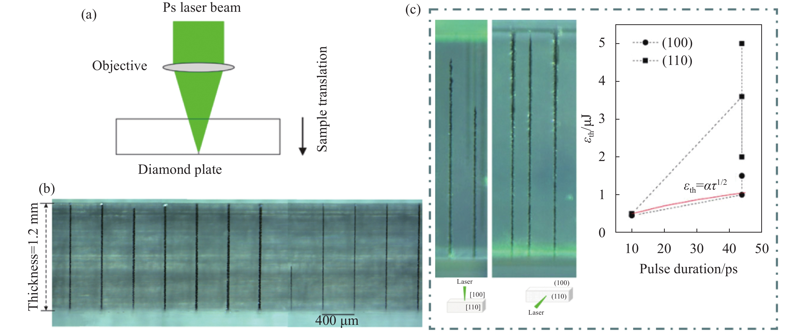
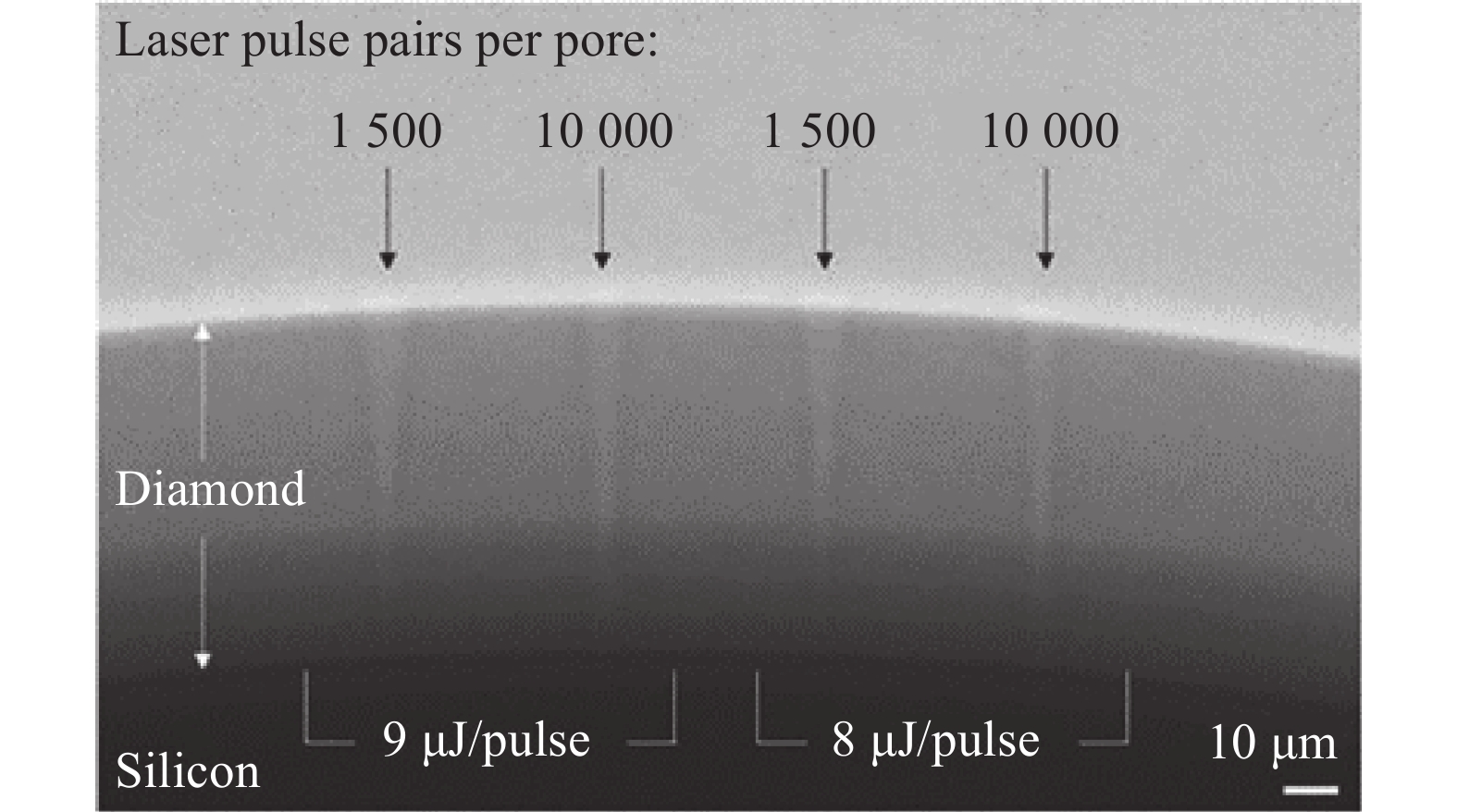
目前,国内外用于金刚石微孔加工的方法主要有激光刻蚀和等离子刻蚀,后者对于大量微孔的同时制备有更好的适用性,但刻蚀工艺尚不成熟且难以完成深孔加工,激光加工金刚石成为了快速微孔成型的首选。B. Jeong[67]等使用自制的飞秒(1030 nm;230 fs)Yb:KGW激光进行金刚石微孔的加工,分析了脉冲能量和脉冲数对微孔孔径、锥角及微孔质量的影响。Aiden A. Martin[68]等使用双脉冲激光烧蚀硅球衬底上的金刚石材料以制备金刚石微孔,见图17,微孔横穿金刚石层于上表面呈现漏斗状锥形,在表面和50%深度处测量的深宽比分别为8∶1和14.5∶1。但由于加工的金刚石薄膜厚度较薄(65 μm),对于实际加工的普适性不强。Natalie C. Golota[69]等使用纳秒激光(532 nm;20 ns)对金刚石进行打孔实验,在脉冲数为10000时最大深宽比为22∶1,通过进一步增大脉冲累积数量获得的最大深宽比大于40∶1,如图18所示。

国内也有多家单位进行了金刚石激光微孔成型的研究,西安交通大学王宏兴[70]等研究了飞秒激光加工高深宽比微孔过程的结构及元素演变,当激光曝光时间为100 s,功率为60 mW时,得到了深宽比为15∶1的微孔。总体而言,深宽比在12~15∶1的金刚石微孔加工报道较多,而使用飞秒激光或贝塞尔激光可以实现的深宽比高达500∶1[67-68, 71]。
笔者课题组董春燕[72]对不同激光功率下的金刚石微孔成型及缺陷特征进行研究,结果表明:当高功率激光照射时微孔外表面出现破损而内表面出现明显的条纹状结构,激光加工过程中对微孔内表面的应力影响大于微孔的边缘位置。
控制微孔精度和避免材料损伤是金刚石激光打孔的关键。更为精准的激光聚焦技术是提高孔径形状控制的直接手段。
-
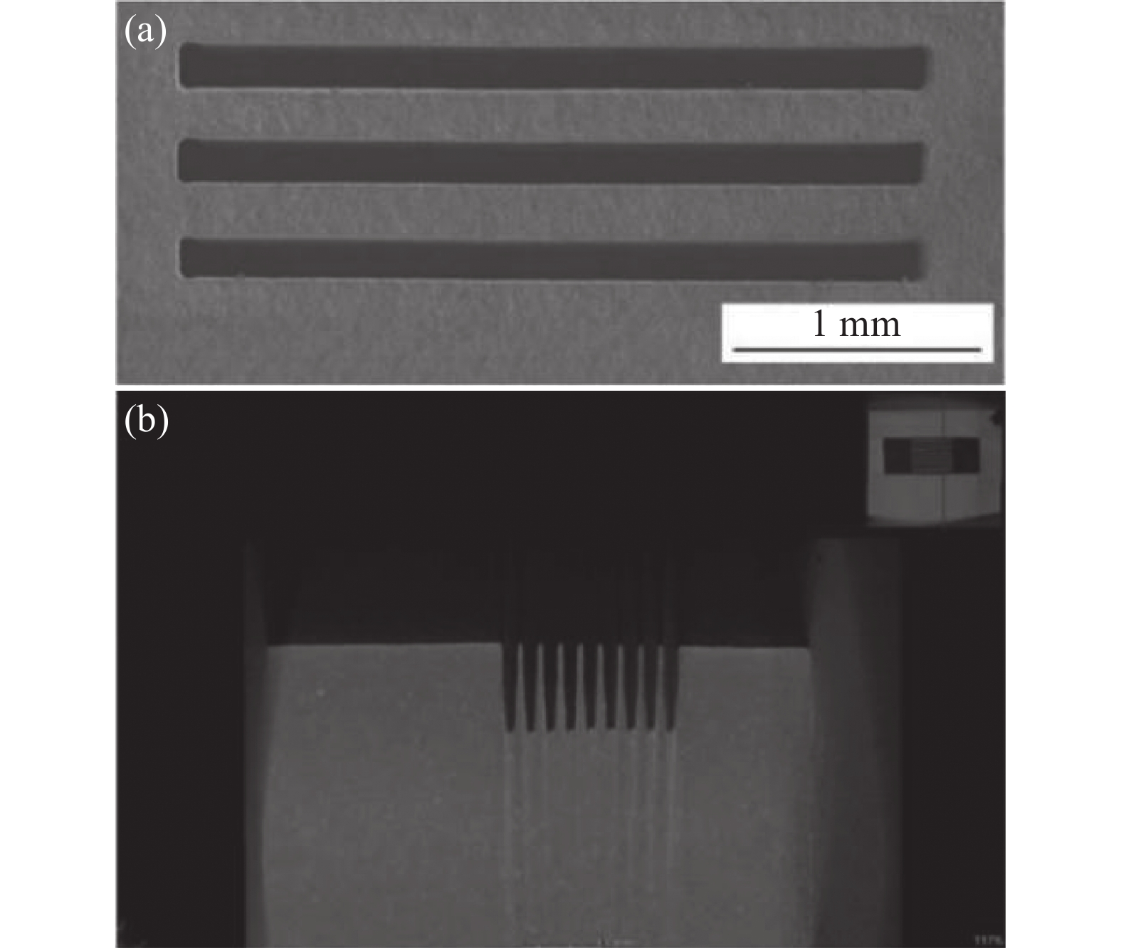
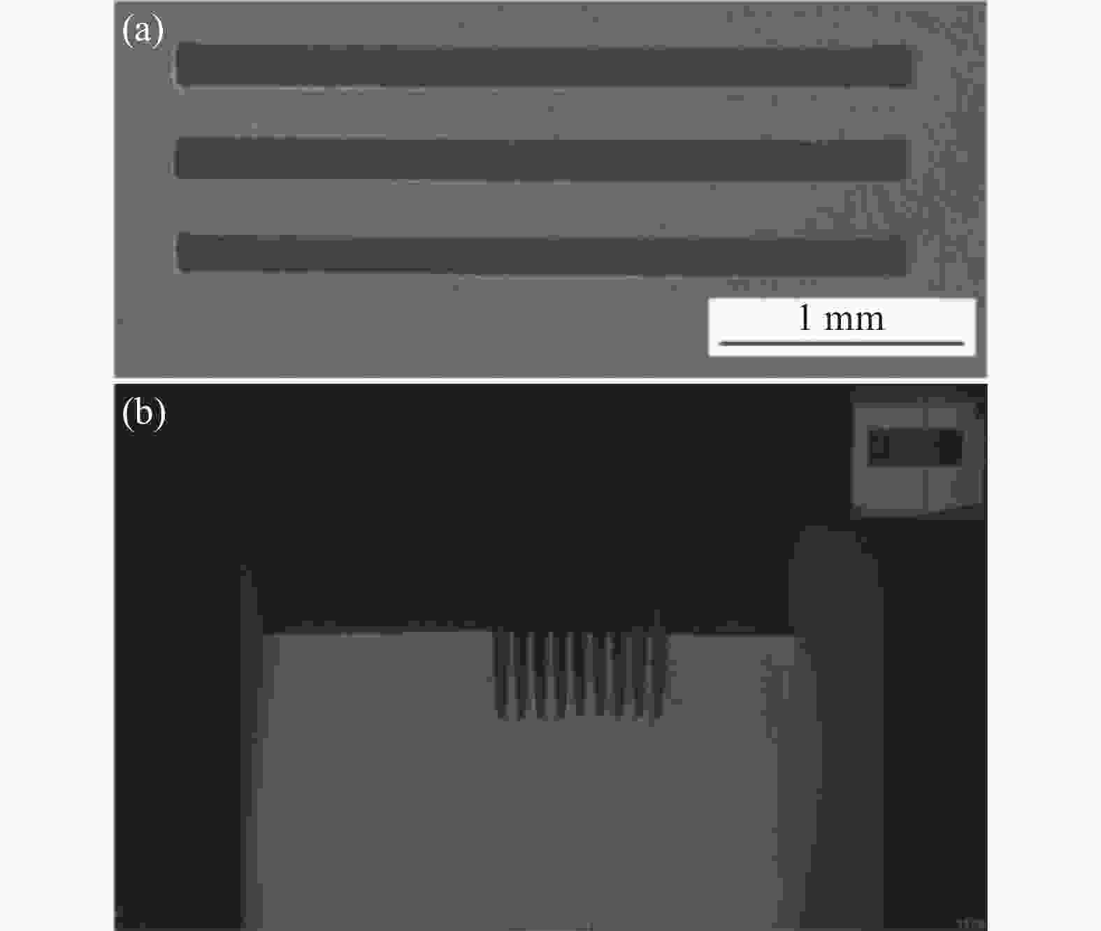
金刚石微槽道结构能够满足航空航天、电子化工等领域对散热性能方面的迫切需求,激光加工是目前加工金刚石微槽道的主流方法,微槽道结构的关键是切割加工出具有高准直度、表面质量良好的凹槽。姜海涛[26]等在模拟仿真的基础上探究了工艺参数对金刚石加工微槽尺寸影响的规律,在优化工艺下成功加工出锥度小于3°的微流道结构,如图19所示。韦新宇[73]等使用紫外纳秒激光在单晶CVD金刚石上加工微槽,经过工艺参数的优化可以加工出表面一致性好,边缘完整,无裂纹和崩边及微槽深度和表面宽度较大的金刚石微槽。黄建衡[74]等基于飞秒激光加工技术在高质量多晶金刚石表面形成微结构阵列,其槽宽为20 μm,槽深达到45 μm,这为实现X射线成像提供了光源器件。笔者课题组也致力于金刚石微槽道散热制备与热沉性能研究,齐志娜[41]使用高能激光束流烧蚀制备了超厚金刚石微通道,基于单相传热系统,金刚石微通道热沉的导热系数在5637.1~11447.2 W/(m2·K),这比相同形状的铝微通道热沉高出了37%~73%,相对应的转化为热沉中流体体积流量,金刚石热沉的流量需求可降低40%。此外,笔者课题组凃军磊[75]在齐志娜工作的基础上制备了z型歧管式全金刚石微通道,同样通过高能激光烧蚀分别制得分流基板和微槽基板,将其组装构成歧管式金刚石微通道,如图20所示,进一步提高了金刚石散热器件热沉性能。
反观国外,Mariusz Dudek[76]等人使用纳秒激光器(355 nm)加工出了带有不同微观结构的多晶金刚石样品,得到的微观结构几何形状精确,垂直度好,通道深,这再次证实了激光用于制造金刚石微流体器件的可行性。不同截面形状的三维金刚石微槽的液固共轭热传数值分析结果表明,矩形微槽比三角形和梯形微槽有更好的传热性能[77]。但在进行大面积微槽加工时,保证整体微槽道深度的一致性是加工过程中关注的要点,Yasuhiro Okamoto[42]等提出了一种两步扫描的方法并将其应用于高质量的单晶金刚石微形状加工。Masataka Shinoda[78]等利用飞秒激光(800 nm;120 fs)在单晶金刚石表面加工出40 nm宽,500 nm深,0.3 mm长的周期性微槽,其深宽比为12∶1,各微槽之间的平均槽距为(146±7) nm。
-
传统的机械研磨方法效率低,易造成环境污染且很难形成自动化工艺,当激光以较大角度入射金刚石表面并以特定路径进行扫描时,也能对粗糙的金刚石表面进行快速去除,从而实现表面快速加工。目前有关激光研磨的研究主要集中在激光入射角度、材料去除速率以及加工表面粗糙度等方面。
Huangang Liu[79]等人将激光束(355 nm;25 ns)垂直照射在单晶金刚石表面,试验在接近烧蚀阈值的激光通量附近进行,在实现金刚石抛光的同时还保证了其较好的光学性质,如图21所示。激光垂直的入射角度需要兼顾离焦量和烧蚀阈值的大小关系,且材料去除速率较低,无法满足高效平整化需求。在将激光应用于激光平整化过程中,采取倾斜激光入射是一种提高加工效率与加工质量的有效方法,徐峰[80]等探究了激光平整化过程中激光(1064 nm;400 ns)入射角度对加工质量的影响,得出结论:较大的入射角度能获得较好的表面粗糙度,但由于实验装置的限制,角度范围只在0°~75°范围内进行,而未对更大的入射角度进行实验。为达到金刚石加工的阈值能量,随着激光入射角度的增大,所需的入射激光能量应当进一步提高。国外也有文献报道更大的激光入射角度[81-82],大多数的角度范围选在75°~85°之间,更大的激光入射角度[83](90°)也有报道,但当入射角度超过某一定值后会由于“阴影效应”在加工表面产生微秒级的周期性条纹[84],限制加工表面粗糙度。
相较于传统的机械研磨平整化金刚石粗糙表面的方法,激光平整化最大的亮点是其极高的加工效率。笔者课题组梁轶凡等对机械研磨金刚石的去除速率进行了研究,随着磨料粒径的增大,研磨的材料去除速率也随着增大,但即使使用粒径60 μm的金刚石粗粉进行研磨,所达到的去除速率也仅有0.2 mm3/min。对比同组的李世谕[9]使用激光进行平整化加工,其材料去除速率提高一个数量级,达到1.1 mm3/min。而使用飞秒激光进行加工时,其加工效率就低得多,Ogawa[60]等对比了纳秒脉冲激光和飞秒脉冲激光加工聚晶金刚石的加工效果,试验结果表明,飞秒激光加工在表面几乎不产生石墨,去除速率仅有0.24 mm3/min。
激光平整化过程除了有较高的去除速率,其加工后表面粗糙度也是目前业内人士关注的重点之一。通常经过激光平整化后金刚石表面粗糙度能降低至几百纳米,甚至在较小的测试范围内其粗糙度达到纳米量级。S. Gloor[85]等通过ArF紫外准分子激光对自支撑320 μm厚的金刚石进行抛光,如图22所示,其粗糙度Ra为0.22 μm (100 μm×100 μm),在更小的测试区域内粗糙度Ra降低至0.12 μm (10 μm×10 μm)。Huagang Liu[79]使用355 nm的纳秒激光对CVD金刚石进行抛光,在测试范围内(20 μm×20 μm)粗糙度Ra可达到8.02 nm。尽管激光平整化后金刚石表面粗糙度有明显的降低,但和传统的机械抛光达到的粗糙度仍存在较大差距。

可以预见的是激光平整化将会取代传统的机械研磨方式,但单一的激光源难以同时满足加工效率与表面质量要求,开发激光分步抛光方法或进一步改进激光控制系统和激光束质量可能是未来的一个重要发展方向。
-
为金刚石半导体化做战略部署,需要开发金刚石薄晶圆制备方法。但金刚石晶圆的硬度远远超过硅,因此无法采用传统的线切割方法完成切片。而离子注入因注入面积和仪器成本的制约在工业应用和科学研究上受到限制。激光剥离技术是将激光精密加工技术与晶体剥离技术相结合,预先在晶体内特定位置制造结合力较薄弱的改质层,有利于剥离工艺中形成确定的晶体断裂位置,从而提升了剥离过程的可控性与晶片的厚度一致性[86],这对于金刚石等高硬度、高脆性、高材料成本的单晶材料加工尤为重要。
T. V. kononenko等发现可以利用红外飞秒激光在金刚石内部制备石墨微结构[30],并通过控制激光照射条件实现了长度为150 μm,直径为1.5 μm的石墨线。这也是激光剥离金刚石晶圆的理论基础,将飞秒激光斑点聚焦于在亚表层形成非金刚石相,再通过化学气相沉积方式进行同质外延生长增厚,最后通过电化学刻蚀剥离的方式实现金刚石薄膜与衬底分离。Wang Fei[87]等基于此方法将单晶金刚石从衬底中分离出来,实验中飞秒激光处理后的金刚石截面如图23所示,在金刚石内部深度约为12 μm处可以清晰的看到非金刚石条带。

飞秒激光加工技术提供了一种将生长的金刚石薄膜与其衬底分离的可能方法。但其加工过程需要在不破坏金刚石基底材料的情况下进行,这要求对激光能量的精确控制。
-
近年来,为了满足金刚石等透明硬质材料的加工需求,研究人员基于传统激光加工方法开发了各种混合激光加工技术。包括混合激光加工方法、水导激光加工及水助激光加工等。
-
当前的激光加工方法大多以单一脉宽形式进行,其存在由激光本征特点决定的各种限制。例如,纳秒、微秒激光加工效率高,但易产生热影响区,易导致材料内部开裂等情况;皮秒与飞秒激光虽能减少热影响区的形成,但其加工效率存在较大限制,难以进行高效加工。单一脉冲的激光加工方法难以达到加工需求,多激光混合加工模式可能有更好效果。Dinesh Kalyanasundaram[88]等设计了CO2激光/水导激光的混合激光加工装置,如图24所示,利用CO2激光进行局部加热;水导激光对加热区进行快速淬火,从而完成聚晶金刚石板材的切割,试验结果表明CO2激光/水导激光混合的激光加工方法能以高于其他切割技术的速度完成高效加工。Malshe A P[89]等在专利中提到采用两种或两种以上波长的激光来对金刚石膜表面进行抛光,即先用Nd:YAG激光或红外光处理材料表面,使材料表面微结构破坏,然后再用波长为193 nm的激光处理结构破坏后的金刚石膜表面,其加工效果相较于单独的YAG激光处理更为理想。
混合激光的加工方式能结合不同类型激光的优势,但通常装置比较复杂,对加工样品限制性较大。对于有特殊需求的高端应用而言仍是未来发展的重要方向。
-
水导激光加工是一种由微细水射流引导激光进行加工的技术。当激光以一定入射角从较高折射率的水射向空气时,会发生全反射。与干式激光切割相比,使用水导激光加工时大部分能量消耗在水中而不是材料中。水射流冷却切割边缘,有效减少了热影响区和热残余应力,防止材料内部的热损伤。这样的加工模式既通过水射流将激光传输至加工表面又带走了多余的热量与残渣。同时,由于激光被限制在水束内从而延伸了激光的焦点,提高轴向加工的加工效率。因此,水导激光对金刚石材料的微结构具有较好的加工特性。
近年来,国内外学者采用水导激光对金刚石类透明硬脆的难加工材料开展了较为深入的研究。石广丰[90]等对比了激光和水导激光对天然金刚石大的加工效果,在加工后的金刚石表面均能观察到一层较薄的碳同素异构体,但水导激光加工的表面仅存在一薄层石墨结构,且产生的产于应力小,微裂纹较少。A. Richmann[91]使用水导激光切割厚达3 mm的蓝宝石,实现了平行壁粗糙度小于0.5 μm,切口宽度小于100 μm的高质量加工。其加工边缘质量高,曲率半径小于20 μm,且无任何切屑。Qiao Hongchao[92]使用水导激光对单晶硅进行微结构加工,切割最高纵横比高达12.7,且很少出现局部断边。
水导激光对金刚石加工有很好的适用性,但仍存在一些技术难点:更细的稳定水射流和水中激光功率的衰减是两个主要问题,此外水导激光打深孔也是一个难点。由于市场竞争和保密方面等问题,很少有关于此方面的文献报道,尤其针对金刚石等超硬材料的水导激光加工的报道更为少见。
-
水助激光与水导激光加工存在明显的差异性,水助激光的关键是通过水的冷却作用,减少激光加工过程中产生的热量。
M. Silvennoinen[93]等基于红外飞秒激光对比了有无水辅助条件下的激光打孔和凹槽烧蚀效果,如图25所示。实验结果表明水助激光加工能更有效的进行孔烧蚀,同时烧蚀孔及周边区域无碎片,保证了烧蚀质量。在水助激光加工过程中,激光束受碎片和悬浮在水中的气泡的影响而散射,同时水层的不连续性和不稳定性均会恶化加工效果。为此,Tangwarodomnukun[94-95]等提出在薄而流动的水层中进行激光烧蚀。国内研究人员基于此基本原理,提出在脉冲激光加工中引入水喷雾从而形成超薄高速流动水膜,并将其应用于金刚石涂层刀具成功制备了微槽阵列(80 μm宽槽阵列)和两种复合微结构(亚毫米尺度结构和8 μm宽槽阵列)。加工过程并没有出现再沉积和涂层脱落等现象[96]。

虽然,液相激光烧蚀技术具有隔绝空气、减少热影响区、减少碎屑堆积等优势,但是液体层吸收会导致激光能量的较大损失。另外,液体层厚度难以精确控制造成结构表面质量均匀性较差。
表3总结了金刚石不同激光加工类型的加工效果,根据加工类型进行分类,一并总结了加工所使用的激光类型及工作亮点。
表 3 激光加工金刚石不同加工类型研究进展
Table 3. Research progress of different processing types of laser processing diamond
Processing type Laser type Highlight Processing result Reference Cutting 193 nm;25 ns Argon gas is injected to change the processing atmosphere Avoid plasma heat damage [64] Cutting 1.06 μm;100 μs The optimum process parameters were determined by orthogonal experiment Section roughness: Ra=0.65 μm; Slit width: 173.1 μm; Taper: 5.9° [66] Drilling 532 nm;20 ns Low taper, high aspect ratio structure Maximum aspect ratio: 66:1; Minimum taper: 0.1°(aspect ratio 10:1) [69] Drilling 1030 nm;230 fs Effect of laser parameters on micropore geometry Micropore no debris, no heat damage [67] Microchannel 800 nm;120 fs Combined with the experiment and simulation, the micro-channel "cold" machining is realized Interface side taper <3°
no residue, crack, edge breakage and other defects on the surface[26] Microchannel 800 nm;100 fs The diamond microstructure array constitutes the X-ray source array anode Microstructure groove width: 20 μm; Groove depth: 45 μm [74] Microchannel 1060 nm;200 ns Microslot linear repeat two scans The bottom of the microgroove is wide and flat [42] Microchannel 800 nm;120 fs Laser induced formation of nanoscale linear grooves Slot width: 40 nm; the groove depth is 500 nm;
Length: 0.3 mm; Average spacing: (146±7) nm[78] Planarization 355 nm;25 ns Laser polishing is directly used in optical device manufacturing Roughness Ra= 8.02 nm (20× 20 μm2); The light transmittance reaches 47.1% [79] Planarization 1.06 μm;100 μs High efficiency flat rough diamond surface Surface roughness Sa= 1.9 μm; material removal rate 1.1mm3/min [9] Separation 800 nm;50 fs The laser forms a non-diamond phase on the subsurface Electrochemical stripping is achieved after epitaxial thickening [87] Hybrid laser CO2 laser/water guided laser The CO2 laser is processed and the water guided laser is used to quench the heating zone Cut sheets faster [88] Water guided laser ------ The waterway extends the laser focus and improves the axial processing efficiency With a carbon layer formed only on the surface, stress is reduced [90] Water-assisted laser 790 nm;120 fs Water mist assisted infrared laser ablation No self-organizing structure is generated [93] Water-assisted laser 532 nm;652 ps CVD diamond-coated tools are used to process cross-scale microstructures The precise microslot array and two composite microstructures were prepared [96] -
激光加工作为一种高效的加工金刚石方法,近几年收到业界人士的广泛关注。但目前仍面临一些挑战。
1)皮秒和飞秒激光加工金刚石的精度和质量较高,但加工效率较低,而毫秒和纳秒激光的脉冲持续时间较长,在加工过程中不可避免地形成热影响区进而产生缺陷,无法满足金刚石高质量加工需求。需要优化激光工艺参数,使得加工过程中保证较高材料去除速率的同时拥有质量较高的加工表面,并进一步减少加工样品中热影响区的产生。
2)激光抛光金刚石总伴随着热应力及变形问题,尤其对于自支撑的大尺寸金刚石薄膜,在加工过程中由于热量的累积以及材料去除过程中应力的释放不可避免地增加了金刚石晶圆的变形,给后续应用及加工带来困难。
3)对于光学级及电子级的高质量金刚石,激光加工会在金刚石表面或亚表层引入缺陷,恶化其光学及电学性能。激光加工损伤问题是目前限制激光加工金刚石领域扩展的关键点之一。
虽然激光加工金刚石还存在许多问题,但未来激光加工仍会是金刚石加工领域的主要技术之一。激光加工技术也会更加成熟以满足各种加工需求,并逐渐向高效、高精度、低损伤、高度集成及生产自动化方面发展。在可预见的未来,激光加工金刚石的应用前景一定会越来越广阔。
Research and application progress of laser technology in diamond processing
-
摘要: 激光加工是目前金刚石的主流加工方法,相较于传统的机械加工形式,激光加工精度高、效率高、普适性强,因而在金刚石切割、微孔成型、微槽道加工及平整化等方面均得到广泛应用。文中阐述了金刚石激光加工原理,介绍了不同类型激光与金刚石材料相互作用机制,重点总结了近几年多种激光加工金刚石模式的发展现状,分析了新型的激光加工方法的特点,探讨了现阶段激光技术在金刚石加工领域面临的问题、挑战及未来的发展趋势。Abstract:
Significance As an efficient non-contact processing method, laser processing is an ideal processing method for super-hard brittle materials such as diamond. The high-energy laser ablation of diamond greatly improves the processing efficiency of diamond, and the ultra-fast laser processing of diamond ensures the processing accuracy to the greatest extent. At present, laser is widely used in diamond cutting, lapping, micro-grooves and other aspects. Clear diamond laser interaction mechanism and processing control mechanism for laser processing diamond industrial investment laid a foundation. Due to the limitations of traditional machining methods, laser processing methods at home and abroad are the focus of research and development technology. It is foreseeable that laser processing in the field of diamond processing will have a larger proportion, which is of great significance for the back-end application and assembly of diamond. Progress Firstly, the laser generation mode and laser processing mechanism are introduced, including laser generation and main characteristics, how the diamond absorbs laser energy, and the changes of diamond properties and surface morphology caused by the laser. At present, the main research is nanosecond laser and femtosecond laser, which are currently two typical types of laser used for diamond processing, according to the laser wavelength division commonly used a green laser (532 nm), near infrared laser (1064 nm) and ultraviolet laser. Pulsed laser is the focus of current research, for diamond processing, short wavelength and small pulse duration processing quality is higher, while longer pulse duration pulsed laser processing efficiency is higher. With the development of technology, laser processing systems in various countries are developing in a more compatible direction, that is, to achieve good processing quality and high removal efficiency at the same time. Countries have successfully carried out a number of technical studies in the field of laser diamond processing, which has been widely used in production. According to the investigation and development, the pulse width length of the laser has a decisive impact on the processing effect. For the different processing types of diamond, the multi-method joint processing method is currently used to meet the specific requirements of various tasks. For the actual processing needs of diamond, mainly including laser cutting, laser drilling, laser micro-grooves and lapping and other related fields. According to different processing types, the development status and technical highlights of laser diamond processing in recent years are summarized (Tab. 4). Through comprehensive investigation, the future development trend and common technical means of laser diamond processing are revealed. Laser diamond processing is one of the current mainstream processing methods, and compared with traditional machining methods, laser processing technology can achieve automation, low-cost, high-precision, and can obtain more accurate processing effects. At the end of this paper, the application prospect of laser diamond processing is prospected in order to provide reference for the development and research of domestic super-hard material processing technology. Conclusions and Prospects The field of laser diamond processing is still booming. At the same time, diamond processing needs are complex and diverse. For different processing types and application requirements, the type of laser used, the mode of processing operation and the selection of processing parameters need to be analyzed in detail according to each case. The research progress of laser diamond processing industry in recent years is summarized in order to provide some reference for the design and optimization of laser diamond processing in the future. Laser processing technology will also be more mature to meet a variety of processing needs, and gradually to high efficiency, high precision, low damage, highly integrated and production automation. In the foreseeable future, the application prospect of laser processing diamond will be more and more broad. -
Key words:
- diamond /
- laser processing /
- laser cutting /
- microporous forming /
- microchannel /
- laser flattening
-

图 7 800 nm飞秒激光辐照金刚石表面扫描电镜图片。(a)于3000脉冲激光能量密度1.9 J/cm2形成的170 nm周期性结构;(b)于8000脉冲激光能量密度2.8 J/cm2形成的190 nm周期性结构[36]
Figure 7. Scanning electron microscope images of diamond surface irradiated by 800 nm femtosecond laser. (a) 170 nm periodic structure formed at 3000 pulse laser energy density of 1.9 J/cm2; (b) 190 nm periodic structure formed at 8000 pulse laser energy density of 2.8 J/cm2 [36]


图 10 不同加工方式得到PCD复合材料的聚焦离子束(Focused ions beam, FIB)截面图。(a)研磨;(b)电火花加工;(c)脉宽10 ps激光;(d) 脉宽125 ns激光;(e) 脉宽450 μs激光
Figure 10. FIB cross sections of PCD composites obtained by: (a) Lapping; (b) Wire EDM; (c) Laser when pulse width =10 ps; (d) Laser when pulse width =125 ns; (e) Laser when pulse width =450 μs
图 12 不同激光通量下加工凹坑处的Raman光谱图像
Figure 12. Raman spectral images of machined pits under different laser fluxes
图 13 不同激光能量下皮秒激光烧蚀金刚石微槽中心位置处的拉曼光谱
Figure 13. Raman spectra of picosecond laser ablation of diamond micro-grooves at different laser energies

图 15 200 fs激光加工单晶金刚石表面扫描电镜图。(a)激光脉冲能量为1.2 mJ加工的弯曲结构;(b)激光脉冲能量为840 nJ时的加工表面图像;(c)图(b)的放大图像[59]
Figure 15. Scanning electron microscope images of single crystal diamond surface processed by 200 fs laser. (a) Curved structure processed by laser pulse energy of 1.2 mJ; (b) The machined surface image when the laser pulse energy is 840 nJ; (c) An enlarged image of figure (b)[59]

表 1 金刚石的性质和应用
Table 1. Properties and applications of diamond
Property Value Application Bandgap/eV 5.4 High-temperature electronics Carrier mobility/(cm2·V−1·s−1) Holes 3 800; electrons 4 500 Radiation-hard detectors Optoelectronic switches Resistivity/Ω·cm 1013-1015 Thermal conductivity
/(W·m−1·K−1)2 000-2 400 Heat sinks Dielectric constant 5.7 Optical transmission range 225 nm- radio frequency Photonics and MW devices Hardness/GPa (81±18) Tools, surgery blades Acoustic wave velocity/(km·s−1) 18.4 along <100> Surface acoustic wave devices Thermal expansion coefficient
/(10−6 ·K−1)0.8(293 K) Photonics and MW devices Corrosion resistance Stable in HF Electrochemistry Negative electron affinity Electron emitters Biocompatibility Biomedicine  下载: 导出CSV
表 2 用于金刚石加工的激光种类
Table 2. Types of laser used in diamond processing
Type Nd:YAG Ti:Al2O3 Cu Ar+ KrF ArF CO2 Wavelength/nm 1 064 532 800 510.5 488 248 193 10 600 Energy/eV 1.17 2.33 1.55 2.42 2.54 5.0 6.42 0.12 Mode Pulse/continuous Pulse Pulse Continuous Pulse Pulse Pulse
下载: 导出CSV
表 3 激光加工金刚石不同加工类型研究进展
Table 3. Research progress of different processing types of laser processing diamond
Processing type Laser type Highlight Processing result Reference Cutting 193 nm;25 ns Argon gas is injected to change the processing atmosphere Avoid plasma heat damage [64] Cutting 1.06 μm;100 μs The optimum process parameters were determined by orthogonal experiment Section roughness: Ra=0.65 μm; Slit width: 173.1 μm; Taper: 5.9° [66] Drilling 532 nm;20 ns Low taper, high aspect ratio structure Maximum aspect ratio: 66:1; Minimum taper: 0.1°(aspect ratio 10:1) [69] Drilling 1030 nm;230 fs Effect of laser parameters on micropore geometry Micropore no debris, no heat damage [67] Microchannel 800 nm;120 fs Combined with the experiment and simulation, the micro-channel "cold" machining is realized Interface side taper <3°
no residue, crack, edge breakage and other defects on the surface[26] Microchannel 800 nm;100 fs The diamond microstructure array constitutes the X-ray source array anode Microstructure groove width: 20 μm; Groove depth: 45 μm [74] Microchannel 1060 nm;200 ns Microslot linear repeat two scans The bottom of the microgroove is wide and flat [42] Microchannel 800 nm;120 fs Laser induced formation of nanoscale linear grooves Slot width: 40 nm; the groove depth is 500 nm;
Length: 0.3 mm; Average spacing: (146±7) nm[78] Planarization 355 nm;25 ns Laser polishing is directly used in optical device manufacturing Roughness Ra= 8.02 nm (20× 20 μm2); The light transmittance reaches 47.1% [79] Planarization 1.06 μm;100 μs High efficiency flat rough diamond surface Surface roughness Sa= 1.9 μm; material removal rate 1.1mm3/min [9] Separation 800 nm;50 fs The laser forms a non-diamond phase on the subsurface Electrochemical stripping is achieved after epitaxial thickening [87] Hybrid laser CO2 laser/water guided laser The CO2 laser is processed and the water guided laser is used to quench the heating zone Cut sheets faster [88] Water guided laser ------ The waterway extends the laser focus and improves the axial processing efficiency With a carbon layer formed only on the surface, stress is reduced [90] Water-assisted laser 790 nm;120 fs Water mist assisted infrared laser ablation No self-organizing structure is generated [93] Water-assisted laser 532 nm;652 ps CVD diamond-coated tools are used to process cross-scale microstructures The precise microslot array and two composite microstructures were prepared [96]
下载: 导出CSV
-
[1] Guo Jiang, Zhang Jianguo, Pan Yanan, et al. A critical review on the chemical wear and wear suppression of diamond tools in diamond cutting of ferrous metals [J]. International Journal of Extreme Manufacturing, 2020, 2(1): 1-24. [2] 袁明文 . 金刚石电子器件的研究进展 [J]. 微纳电子技术,2012 ,49 (10 ):643 -649 . Yuan Mingwen. Research Progress of Diamond Based Electronic Devices [J]. Micronanoelectronic Technology, 2012, 49(10): 643-649. (in Chinese)[3] Kiss Marcell, Mi Sichen, Huszka Gergely, et al. Diamond diffractive optics—recent progress and perspectives [J]. Advanced Optical Technologies, 2021, 10(1): 19-30. doi: 10.1515/aot-2020-0052 [4] Wang D, Zhao W S, Gu L, et al. A study on micro-hole machining of polycrystalline diamond by micro-electrical discharge machining [J]. Journal of Materials Processing Technology, 2011, 211(1): 3-11. doi: 10.1016/j.jmatprotec.2010.07.034 [5] Axinte D A, Srinivasu D S, Kong M C, et al. Abrasive waterjet cutting of polycrystalline diamond: A preliminary investigation [J]. International Journal of Machine Tools and Manufacture, 2009, 49(10): 797-803. doi: 10.1016/j.ijmachtools.2009.04.003 [6] Subramani K, Vasudevan A, Karthik K, et al. Insights of abrasive water jet polishing process characteristics and its advancements [J]. Materials Today: Proceedings, 2022, 52: 1113-1120. doi: 10.1016/j.matpr.2021.11.005 [7] 郭世斌, 曲杨, 吕反修, 等 . 大面积金刚石自支撑膜机械抛光的优化工艺研究 [J]. 功能材料,2007 (07 ):1173 -1175 . Guo Shibin, Qu Yang, Lv Fanxiu, et al. The study on the optimizational technology of the large area free-standing diamond films’ mechanical polishing [J]. Journal of Functional Materials, 2007(07): 1173-1175. (in Chinese)[8] Zheng Yuting, Cumont A E L, Bai Mingjie, et al. Smoothing of single crystal diamond by high-speed three-dimensional dynamic friction polishing: Optimization and surface bonds evolution mechanism[J]. International Journal of Refractory Metals and Hard Materials, 2021, 96: 105472. [9] 李世谕, 安康, 邵思武, 等 . CVD金刚石膜激光平整化效率和粗糙度 [J]. 金刚石与磨料磨具工程,2022 ,42 (01 ):61 -68 . Li Shiyu, An Kang, Shao Siwu, et al. Laser planarization efficiency and roughness of CVD diamond film [J]. Diamond & Abrasives Engineering, 2022, 42(1): 61-68.[10] Ohfuji H, Okuchi T, Odake S, et al. Micro-/nanostructural investigation of laser-cut surfaces of single- and polycrystalline diamonds [J]. Diamond and Related Materials, 2010, 19(7-9): 1040-1051. doi: 10.1016/j.diamond.2010.02.015 [11] Jiang Tong, Gao Si, Tian Zhennan, et al. Fabrication of diamond ultra-fine structures by femtosecond laser [J]. Chinese Optics Letters , 2020, 18(10): 38-42. doi: 10.3788/COL202018.101402 [12] Yang Liangliang, Wei Jiangtao, Ma Zhe, et al. The fabrication of micro/nano structures by laser machining [J]. Nanomaterials (Basel), 2019, 9(12): 1789. doi: 10.3390/nano9121789 [13] Konov V I. Laser in micro and nanoprocessing of diamond materials [J]. Laser & Photonics Reviews, 2012, 6(6): 739-766. [14] 卢康, 许竞翔, 孙强, 等. 金刚石材料石墨化相变诱导机制研究进展[J]. 中国材料进展, 2022, 41(07): 536-546. doi: 10.7502/j.issn.1674-3962.202012028 Lu Kang, Xu Jingxiang, Sun Qiang, et al Research Progress on lnduction Mechanism of Graphitization Phase Transition of Diamond Materials[J]. Materials China , 2022, 41(07): 536-546. (in Chinese) doi: 10.7502/j.issn.1674-3962.202012028 [15] 周炳琨. 激光原理[M]. 第6版. 北京: 国防工业出版社, 2009. [16] 崔涵. 无序光纤结构中激光脉冲的产生及优化 [D]; 电子科技大学, 2020. Cui Han. Generation optimization of laser pulse in disordered fiber structure[D]. Chengdu: University of Electronic Science and Technology of China, 2020. [17] 任彦宇. 窄线宽激光器及其在Φ-OTDR中的应用研究 [D]; 太原理工大学, 2022. Ren Yanyu. Narrow line-width laser and application study in phase sensitive optical time domain reflectometer[D]. Taiyuan: Taiyuan University of Technology, 2022. [18] 杜雯. 固体激光器中激光介质热传导方程的解析研究 [D]; 西安工业大学, 2023. Du Wen. Analytical study of laser medium heat conduction-equation in solid-state[D]. Xi’an: Xi'an Technological University, 2023. [19] Korneychuk S, Guzzinati G, Verbeeck J. Measurement of the indirect band gap of diamond with EELS in STEM[J]. Physica Status Solidi(A), 2018, 215(22): 1800318. [20] Granger M C, Witek M, Xu J, et al. Standard electrochemical behavior of high-quality, boron-doped polycrystalline diamond thin-film electrodes [J]. Anal Chem, 2000, 72(16): 3793-3804. doi: 10.1021/ac0000675 [21] Hermani J-P, Brecher C, Emonts M. Nanosecond laser processing of diamond materials[C]//Lasers in Manufacturing Conference 2015, 2015. [22] 姜玺阳, 王飞飞, 周伟, 等 飞秒激光与材料相互作用中的超快动力学 [J]. 中国激光, 2022, 49(22): 2200001. doi: 10.3788/CJL202249.2200001 Jiang Xiyang, Wang Feifei, Zhou Wei, et al. Ultrafast Dynamics of Femtosecond Laser Interaction with Materials[J]. Chinese Journal of Lasers , 2022, 49(22): 2200001. (in Chinese) doi: 10.3788/CJL202249.2200001 [23] 王海航, 马玉平, 武晓龙, 等 . 金刚石涂层激光抛光机理及加工工艺研究进展 [J]. 材料保护,2021 ,54 (06 ):136 -146 . Wang Haihang, Ma Yuping, Wuxiaolong, et al. Research progress on laser polishing mechanism and processing technology of diamond coating[J]. Materials Protection, 2021, 54(6): 136-146. (in Chinese)[24] 熊彪, 陈根余, 殷赳, 等 . 飞秒激光加工单晶金刚石锥形阵列的试验研究 [J]. 应用激光,2018 ,38 (02 ):270 -277 . Xiong Biao, Chen Genyu, Yin Jiu, et al. Experimental research on conical array of single crystal diamond based on femtosecond laser [J]. Applied Laser, 2018, 38(2): 270-277. (in Chinese)[25] Komlenok M S, Kononenko V V, Ralchenko V G, et al. Laser induced nanoablation of diamond materials[J]. Physics Procedia, 2011, 12: 37-45. doi: 10.1016/j.phpro.2011.03.103 [26] 姜海涛,崔健磊,殷东平等 . 雷达功率组件的金刚石微通道热沉激光加工工艺 [J]. 中国机械工程,2022 , 32(03 ):261 -268 . Jiang Haitao, Cui Jianlei, Yin Dongping, et al. Femtosecond laser processing technology of diamond micro-channel heat sink based on radar power module[J]. China Mechanical Engineering, 2022, 32(3): 261-268. (in Chinese)[27] 闫雄伯. CVD金刚石自支撑膜的高温石墨化行为研究 [D]; 北京科技大学, 2019. Yan Xiongbo. Graphitization behavior of CVD free-standing diamond films at high temperature [D]. Beijing: University of Science and Technology Beijing, 2019. (in Chinese) [28] Smedley J, Bohon J, Wu Q, et al. Laser patterning of diamond. Part I. Characterization of surface morphology [J]. Journal of Applied Physics , 2009, 105(12): 123107. doi: 10.1063/1.3152956 [29] Kononenko T V, Pivovarov P A, Khomich A A, et al. Effect of absorbing coating on ablation of diamond by IR laser pulses [J]. Quantum Electronics, 2018, 48(3): 244-250. doi: 10.1070/QEL16567 [30] Kononenko T V, Meier M, Komlenok M S, et al. Microstructuring of diamond bulk by IR femtosecond laser pulses [J]. Applied Physics A, 2007, 90(4): 645-651. [31] Kononenko T V, Pivovarov P A, Khomich A A, et al. Processing of polycrystalline diamond surface by IR laser pulses without interior damage [J]. Optics & Laser Technology, 2019, 117: 87-93. [32] Liu Yan, Chen Gengxu, Song Min, et al. Fabrication of nitrogen vacancy color centers by femtosecond pulse laser illumination [J]. Opt Express, 2013, 21(10): 12843-12848. doi: 10.1364/OE.21.012843 [33] Kononenko V V, Vlasov I I, Gololobov V M, et al. Nitrogen-vacancy defects in diamond produced by femtosecond laser nanoablation technique [J]. Applied Physics Letters, 2017, 111(8): 081101. [34] Dumitru G, Romano V, Weber H P, et al. Femtosecond ablation of ultrahard materials [J]. Applied Physics A: Materials Science & Processing, 2002, 74(6): 729-739. [35] Forster M, Huber C, Armbruster O, et al. 50-nanometer femtosecond pulse laser induced periodic surface structures on nitrogen-doped diamond [J]. Diamond and Related Materials, 2017, 74: 114-118. doi: 10.1016/j.diamond.2017.02.016 [36] Huang Min, Zhao Fuli, Cheng Ya, et al. Mechanisms of ultrafast laser-induced deep-subwavelength gratings on graphite and diamond [J]. Physical Review B, 2009, 79(12): 125436. [37] Mastellone M, Bellucci A, Girolami M, et al. Deep-Subwavelength 2D periodic surface nanostructures on diamond by double-pulse femtosecond laser irradiation[J]. Nano Lett, 2021, 21(10): 4477-4483. doi: 10.1021/acs.nanolett.1c01310 [38] 江海河 . 激光加工技术应用的发展及展望 [J]. 光电子技术与信息,2001 (04 ):1 -12 . Jiang Haihe. Development and forecast of the laser processing technology application [J]. Journal of Atmospheric and Environmental, 2001(4): 1-12. (in Chinese)[39] Chichkov B N, Momma C, Nolte S, et al. Femtosecond, picosecond and nanosecond laser ablation of solids [J]. Applied Physics A, 1996, 63(2): 109-115. doi: 10.1007/BF01567637 [40] 张少军, 郭智, 成加皿, 等. 高重频硬X射线自由电子激光脉冲到达时间诊断方法研究 [J]. 物理学报, 2023, 72(10): 262-272. Zhang Shaojun, Guo Zhi, Cheng Jiamin, et al. Arrival time diagnosis method of high refrequency hard X-ray free electron laser[J]. Acta Physica Sinica, 2023, 72(10): 262-272. (in Chinese) [41] Qi Zhina, Zheng Yuting, Zhu Xiaohua, et al. An ultra-thick all-diamond microchannel heat sink for single-phase heat transmission efficiency enhancement[J]. Vacuum, 2020, 177: 1-7. [42] Okamoto Yasuhiro, Okubo Tubas, Kajitani Atsuya, et al. High-quality micro-shape fabrication of monocrystalline diamond by nanosecond pulsed laser and acid cleaning [J]. International Journal of Extreme Manufacturing, 2022, 4(2): 025301. doi: 10.1088/2631-7990/ac5a6a [43] Eberle G, Jefimovs K, Wegener K. Characterisation of thermal influences after laser processing polycrystalline diamond composites using long to ultrashort pulse durations [J]. Precision Engineering, 2015, 39: 16-24. doi: 10.1016/j.precisioneng.2014.06.008 [44] Mao Bo, Siddaiah Arpith, Liao Yiliang, et al. Laser surface texturing and related techniques for enhancing tribological performance of engineering materials: A review [J]. Journal of Manufacturing Processes, 2020, 53: 153-173. doi: 10.1016/j.jmapro.2020.02.009 [45] Zhang Zhen, Zhang Quanli, Wang Yeqing, et al. Modeling of the temperature field in nanosecond pulsed laser ablation of single crystalline diamond [J]. Diamond and Related Materials, 2021, 116: 108402. [46] Takayama N, Yan J. Mechanisms of micro-groove formation on single-crystal diamond by a nanosecond pulsed laser[J]. Journal of Materials Processing Technology, 2017, 243: 299-311. doi: 10.1016/j.jmatprotec.2016.12.032 [47] Cadot G B J, Thomas K, Best J P, et al. Investigation of the microstructure change due to phase transition in nanosecond pulsed laser processing of diamond [J]. Carbon, 2018, 127: 349-365. doi: 10.1016/j.carbon.2017.10.030 [48] Kononenko T V, Kononenko V V, Pimenov S M, et al. Effects of pulse duration in laser processing of diamond-like carbon films [J]. Diamond and Related Materials, 2005, 14(8): 1368-1376. doi: 10.1016/j.diamond.2005.02.009 [49] 温秋玲, 韦新宇, 王华禄, 等 . 皮秒激光加工CVD单晶金刚石的特征和机理研究[J]. 光子学报,2021 ,50 (6 ):126 -136 . doi: 10.3788/gzxb20215006.0650113 Wen Qiuling, Wei Xinyu, Wang Hualu, et al. Characteristics and mechanism of CVD single crystal diamond processed by picosecond laser[J]. Acta Photonica Sinica, 2021, 50(6): 126-136. (in Chinese) doi: 10.3788/gzxb20215006.0650113[50] Takayama N, Ishizuka J, Yan J. Microgrooving of a single-crystal diamond tool using a picosecond pulsed laser and some cutting tests [J]. Precision Engineering, 2018, 53: 252-262. doi: 10.1016/j.precisioneng.2018.04.009 [51] Pimenov S M, Khomich A A, Neuenschwander B, et al. Picosecond-laser bulk modification induced enhancement of nitrogen-vacancy luminescence in diamond[J]. Journal of the Optical Society of America B, 2016, 33(3): B49-B55. [52] Pimenov S M, Neuenschwander B, Jäggi B, et al. Effect of crystal orientation on picosecond-laser bulk microstructuring and Raman lasing in diamond[J]. Applied Physics A, 2013, 114(4): 1309-1319. [53] Pimenov S M, Vlasov I I, Khomich A A, et al. Picosecond-laser-induced structural modifications in the bulk of single-crystal diamond [J]. Applied Physics A, 2011, 105(3): 673-637. doi: 10.1007/s00339-011-6645-0 [54] Fork R L, Greene B I, Shank C V. Generation of optical pulses shorter than 0.1 psec by colliding pulse mode locking [J]. Applied Physics Letters, 1981, 38(9): 671-672. doi: 10.1063/1.92500 [55] Schaffer C B, Brodeur A, Mazur E. Laser-induced breakdown and damage in bulk transparent materials induced by tightly focused femtosecond laser pulses[J]. Meas Sci Technol, 2001, 12(11): 1784-1794. doi: 10.1088/0957-0233/12/11/305 [56] Gattass R R, Mazur E. Femtosecond laser micromachining in transparent materials [J]. Nature Photonics, 2008, 2(4): 219-225. doi: 10.1038/nphoton.2008.47 [57] Glezer E N, Milosavljevic M, Huang L, et al. Three-dimensional optical storage inside transparent materials [J]. Opt Lett, 1996, 21(24): 2023-2025. doi: 10.1364/OL.21.002023 [58] Qu Meina, Jin Tan, Xie Guizhi, et al. Developing a novel binderless diamond grinding wheel with femtosecond laser ablation and evaluating its performance in grinding soft and brittle materials[J]. Journal of Materials Processing Technology, 2020, 275: 1-9. [59] Zalloum O H, Parrish M, Terekhov A, et al. An amplified femtosecond laser system for material micro-/nanostructuring with an integrated Raman microscope [J]. Rev Sci Instrum, 2010, 81(5): 053906. doi: 10.1063/1.3430073 [60] Ogawa Y, Ota M, Nakamoto K, et al. A study on machining of binder-less polycrystalline diamond by femtosecond pulsed laser for fabrication of micro milling tools [J]. CIRP Annals, 2016, 65(1): 245-248. doi: 10.1016/j.cirp.2016.04.081 [61] 韩源, 马玉平, 王海航, 等 . 飞秒激光刻蚀纳米金刚石涂层材料去除率的研究 [J]. 激光与光电子学进展,2021 ,58 (11 ):1114001 . Han Yuan, Ma Yuping, Wang Haihang, et al. Material removal rate of nano-diamond coating ablated by femtosecond laser[J]. Laser & Optoelectronics Progress, 2021, 58(11): 1114001. (in Chinese)[62] 方向阳 . CVD金刚石膜激光铲平切割工艺研究 [J]. 宁夏工程技术,2003 (02 ):157 -160 . doi: 10.3969/j.issn.1671-7244.2003.02.017 Fang Xiangyang. The research on laser cutting technology of CVD diamond film [J]. Ningxia Engineering Technology, 2003,2 (2): 157-160. (in Chinese) doi: 10.3969/j.issn.1671-7244.2003.02.017[63] Wang Ji, Zhang Peng, Zhang Tianrun, et al. Experiments of high frequency laser cutting of chemical vapor deposition diamond with large cutting depth [J]. Optics and Precision Engineering, 2022, 30(1): 89-95. (in Chinese) doi: 10.37188/OPE.20223001.0089 [64] Park J K, Ayres V M, Asmussen J, et al. Precision micromachining of CVD diamond films [J]. Diamond and Related Materials, 2000, 9(3): 1154-1158. [65] Yan Lei, Wu Feifei, Deng Yuheng, et al. Study on laser processing of chemical vapor deposition diamond thick film [J]. Diamond & Abrasives Engineering, 2012, 32(5): 6-9. [66] 郭强, 贾志新, 高坚强, 等 . 聚晶金刚石复合片激光切割工艺研究 [J]. 激光与红外,2017 ,47 (6 ):686 -692 . Guo Qiang, Jia Zhixin, Gao Jianqiang, et al. Technological study on laser cutting of polycrystalline diamond compact [J]. Laser & Infrared, 2017, 47(6): 686-692. (in Chinese)[67] Jeong B, Lee B, Kim J H, et al. Drilling of sub-100 μm hourglass-shaped holes in diamond with femtosecond laser pulses [J]. Quantum Electronics, 2020, 50(2): 201-204. doi: 10.1070/QEL17097 [68] Martin A A, Bishop J, Burnett W, et al. Ultra-high aspect ratio pores milled in diamond via laser, ion and electron beam mediated processes [J]. Diamond and Related Materials, 2020, 105: 107806. doi: 10.1016/j.diamond.2020.107806 [69] Golota N C, Preiss D, Fredin Z P, et al. High aspect ratio diamond nanosecond laser machining [J]. Appl Phys A Mater Sci Process, 2023, 129(7): 490. doi: 10.1007/s00339-023-06755-2 [70] Shen Tianlun, Chen Tao, Si Jinhai, et al.Structural changes during femtosecond laser percussion drilling of high-aspect-ratio diamond microholes[J]. Optical Engineering, 2022, 61 (1): 016103.[71] Kumar S, Eaton S M, Bollani M, et al. Laser surface structuring of diamond with ultrashort Bessel beams[J]. Sci Rep, 2018, 8(1): 14021. doi: 10.1038/s41598-018-32415-0 [72] 董春燕, 张晓宇, 顾德华, 等. 不同激光功率下金刚石微孔成形及缺陷特征[J]. 中国激光, 2023, 50(24): 2402404. Dong Chunyan, Zhang Xiaoyu, Gu Dehua, et al. Analysis of diamond microporous forming characteristics and defects under different laser powers[J]. Chinese Journal of Lasers, 2023, 50(24): 2402404. (in Chinese) [73] 韦新宇, 温秋玲, 陆静, 等 . 紫外纳秒激光加工金刚石微槽工艺参数优化研究[J]. 中国激光,2022 ,49 (10 ):1002406 . Wei Xinyu, Wen Qiuling, Lu Jing, et al. Research on parameters optimization of diamond microgrooves processed by ultravilot nanosecond laser[J]. Chinese Journal of Lasers, 2022, 49(10): 1002406. (in Chinese)[74] 黄建衡, 梁国文, 李冀, 等 . 飞秒激光制备多晶金刚石微结构阵列[J]. 中国激光,2017 ,44 (3 ):0302007 . Huang Jianheng, Liang Guowen, Li Ji, et al. Femtosecond laser processing of polycrystalline diamond micro-structure array[J]. Chinese Journal of Lasers, 2017, 44(3): 0302007. (in Chinese)[75] Tu Junlei, Shi Jiadong, Chen Liangxian, et al. Surface termination of the diamond microchannel and single-phase heat transfer performance[J]. International Journal of Heat and Mass Transfer, 2022, 199: 123481. doi: 10.1016/j.ijheatmasstransfer.2022.123481 [76] Dudek M, Rosowski A, Kozanecki M, et al. Microstructures manufactured in diamond by use of laser micromachining[J]. Materials (Basel), 2020, 13(5): 1199. doi: 10.3390/ma13051199 [77] Dou Jian, Cui Jianlei, Fang Xuyang, et al. Theoretical and experimental study on machining rectangular microgroove of diamond by femtosecond laser[J]. Integrated Ferroelectrics, 2020, 208(1): 104-116. doi: 10.1080/10584587.2020.1728722 [78] Shinoda M, Gattass R R, Mazur E. Femtosecond laser-induced formation of nanometer-width grooves on synthetic single-crystal diamond surfaces[J]. Journal of Applied Physics, 2009, 105(5): 053102. doi: 10.1063/1.3079512 [79] Liu Huagang, Xie Linran, Lin Wenxiong, et al. Optical quality laser polishing of CVD diamond by UV pulsed laser irradiation[J]. Advanced Optical Materials, 2021, 9(21): 2100537. doi: 10.1002/adom.202100537 [80] Xu Feng. Study on laser processing and machining of CVD diamond thick-film[D]. Nanjing: Nanjing University of Aeronautics and Astronautics, 2002. (in Chinese) [81] Prieske M, Vollertsen F. Picosecond-laser polishing of CVD-diamond coatings without graphite formation [J]. Materials Today: Proceedings, 2021, 40: 1-4. doi: 10.1016/j.matpr.2020.01.283 [82] Komlenok M, Pashinin V, Sedov V, et al. Femtosecond and nanosecond laser polishing of rough polycrystalline diamond [J]. Laser Physics, 2022, 32(8): 084003. [83] Tsai H Y, Ting C J, Chou C P. Evaluation research of polishing methods for large area diamond films produced by chemical vapor deposition [J]. Diamond and Related Materials, 2007, 16(2): 253-261. doi: 10.1016/j.diamond.2006.06.007 [84] Tosin P, Blatter A, Lüthy W. Laser‐induced surface structures on diamond films [J]. Journal of Applied Physics, 1995, 78: 3797-3800. doi: 10.1063/1.359893 [85] Gloor S, Lüthy W, Weber H P, et al. UV laser polishing of thick diamond films for IR windows [J]. Applied Surface Science, 1999, 135-139. [86] 胡北辰, 张志耀, 张红梅, 等. SiC单晶材料的激光剥离技术研究进展[J]. 电子工艺技术, 2022, 43(4): 192 -195. Hu Beichen, Zhang Zhiyao, Zhang Hongmei, et al. Research progress of laser-assisted spalling for SiC single crystal [J]. Electronics Process Technology, 2022, 43(4): 192 -195. (in Chinese) [87] Wang Fei, Shan Chao, Yan Jianping, et al. Application of femtosecond laser technique in single crystal diamond film separation [J]. Diamond and Related Materials, 2016, 63: 69-74. doi: 10.1016/j.diamond.2015.11.015 [88] Kalyanasundaram D, Schmidt A, Molian P, et al. Hybrid CO2 Laser/Waterjet machining of polycrystalline diamond substrate: Material separation through transformation induced controlled fracture[J]. Journal of Manufacturing Science and Engineering, 2014, 136(4): 041001. doi: 10.1115/1.4027304 [89] Malshe A P, Ozkan A M, Brown W D. Process for sequential multi-beam laser processing of materials: America, US006168744B1 [P]. 2001-01-02. [90] Shi Guangfeng, Han Dongdong, Wang Shukun, et al. Analysis and evaluation of natural diamond cut by water jet-guided laser[J]. Aer Adv Eng Res, 2017, 146: 195-198. [91] Richmann A, Kuzminykh Y, Richerzhagen B, et al. Laser microjet cutting of up to 3 mm thick sapphire[C]//Int Congr Appl Lasers Electro-Optics, 2014: 1139–1143. [92] Qiao Hongchao, Cao Zhihe, Cui Jianfeng, et al, Experimental study on water jet guided laser micro-machining of mono-crystalline silicon[J]. Optics & Laser Technology, 2021, 140: 107507. [93] Silvennoinen M, Kaakkunen J J J, Paivasaari K, et alWater spray assisted ultrashort laser pulse ablation[J]. Applied Surface Science, 2013, 265: 865-869. doi: 10.1016/j.apsusc.2012.11.135 [94] Tangwarodomnukun V, Likhitangsuwat P, Tevinpibanphan O, et al. Laser ablation of titanium alloy under a thin and flowing water layer[J]. Int J Mach Tool Manu, 2015, 89: 14–28. [95] Tangwarodomnukun V, Wuttisarn TEvolution of milled cavity in the multiple laser scans of titanium alloy under a flowing water layer[J]. Int J Adv Manuf Technol, 2017, 92: 293-302. doi: 10.1007/s00170-017-0125-4 [96] Guo Bing, Zhang Jun, Wu Mingtao, et al. Water assisted pulsed laser machining of micro-structured surface on CVD diamond coating tools[J], Journal of Manufacturing Processes, 2020, 56: 591-601. -

 点击查看大图

计量
- 文章访问数: 194
- HTML全文浏览量: 90
- PDF下载量: 75
- 被引次数: 0

