


 下载:
下载:


-
1994年,Era等首次报道了第一个基于二维钙钛矿发光材料的钙钛矿发光二极管(Perovskite Light-Emitting Diodes, PeLEDs)。但是由于当时器件只能在极低温(液氮温度)下工作,很难得到实际应用[1],直到2014年,Friend等人制备出可以在室温下工作的、基于有机-无机金属卤化物钙钛矿的发光材料 CH3-NH3PbBr3(MAPbBr3) 的PeLEDs,才受到越来越多的关注[2]。研究表明,金属卤化物钙钛矿发光材料具有光致发光量子产率高、带隙可调、色纯度高、激子扩散长度长等出类拔萃的光学性能[3-4]。经过研究者们近10年来的努力,采用成分工程[5]、添加剂辅助[6]、结构优化[7]、界面工程[8]、光提取[9]等各种方法,将各类材料:溶剂、有机材料和无机材料;绝缘材料和半导体材料;不发光材料和发光材料等引入PeLEDs中[10–24],实现了薄膜质量的提升、载流子传输的平衡和激子利用率的改善,使PeLEDs的外量子效率(External Quan-tum Efficiency, EQE)由最早的不到1%,到30.84%,实现了30%的超越[25],可以与量子点发光二极管(Quan-tum dot Light-Emitting Diodes, QLEDs)、有机发光二极管(Organic Light-Emitting Diodes, OLEDs)的效率媲美,在照明和显示器方面拥有巨大的潜力。
近5年来,笔者课题组与江苏海洋大学班鑫鑫课题组、苏州大学王照奎课题组合作,致力于将不同类型的有机发光材料引入PeLEDs中,例如,传统的荧光材料、磷光材料、热激活延迟荧光(Thermally Activated Delayed Fluorescence, TADF),封装的热激活延迟荧光树形材料(Encapsulated-TADF dendrimer)、有机热激活延迟荧光聚合物材料(TADF polymer),来钝化薄膜中的缺陷、平衡载流子的传输和提高激子辐射复合效率,以提高PeLEDs的效率和稳定性,将绿光器件PeLEDs的电流效率提高到66.1 cd/A,蓝光PeLEDs的EQE提高到12.38%。
文中首先介绍钙钛矿发光材料的结构,然后阐述激子限制和回收利用的原理,接着详细介绍笔者课题组的若干工作,采用不同种类的有机发光材料作钙钛矿发光薄膜的添加剂或界面缓冲层时,PeLEDs中激子的能量转移机理和器件光电性能提升的物理机理,最后是结论。
-
1839年,德国化学家Gustav Rose在俄罗斯乌拉尔山发现了天然钛酸钙(CaTiO3),为向俄国地质学家Lev Perovski致敬,将其命名为钙钛矿(Perovskite)[26]。随后,科学家们用“钙钛矿”统一指代与CaTiO3结构相似的“ABX3”型材料。元素周期表里,90%的金属元素都可以成为A或B离子,而B和X离子组合成一个八面体,不同的“部件”像搭积木一样组合会产生不同的效果。
-
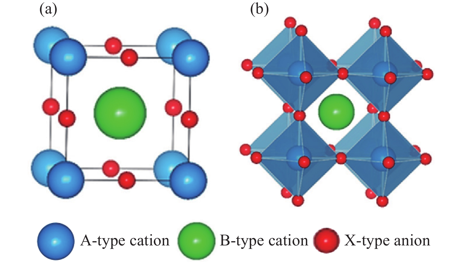
3D金属卤化物钙钛矿结构的通式为“ABX3”,其中,A通常为一价碱金属阳离子/有机阳离子(例如,Cs+、MA+、FA+、CH3NH3+等),B通常为二价金属阳离子(例如,Pb2+、Sn2+等),X通常为卤素阴离子(例如,Cl−、Br−、I−)[27]。其中,B离子和X离子通过配位形成八面体[BX6]4−,而A处于八面体[BX6]4−结构之间的空隙中,在3D空间里扩展就形成了3D钙钛矿结构,如图1所示。笔者课题组前期的工作是基于3D钙钛矿(CsPbBr3)开展的。

图 1 ABX3 金属卤化物钙钛矿的一般晶体结构。 (a) A阳离子占据晶格角,B阳离子占据间隙位,X阴离子占据晶格面心;(b)另一种视角下,B阳离子聚集在X阴离子周围形成[BX6]4−结构[27-28]
Figure 1. ABX3 metal halide perovskite general crystal structure. (a) A-type cations occupy lattice corners, B-type cations occupy interstitial sites, and X-type anions occupy lattice face centers; (b) B-type cations cluster around X-type anions to form [BX6]4− structures[27-28]
-
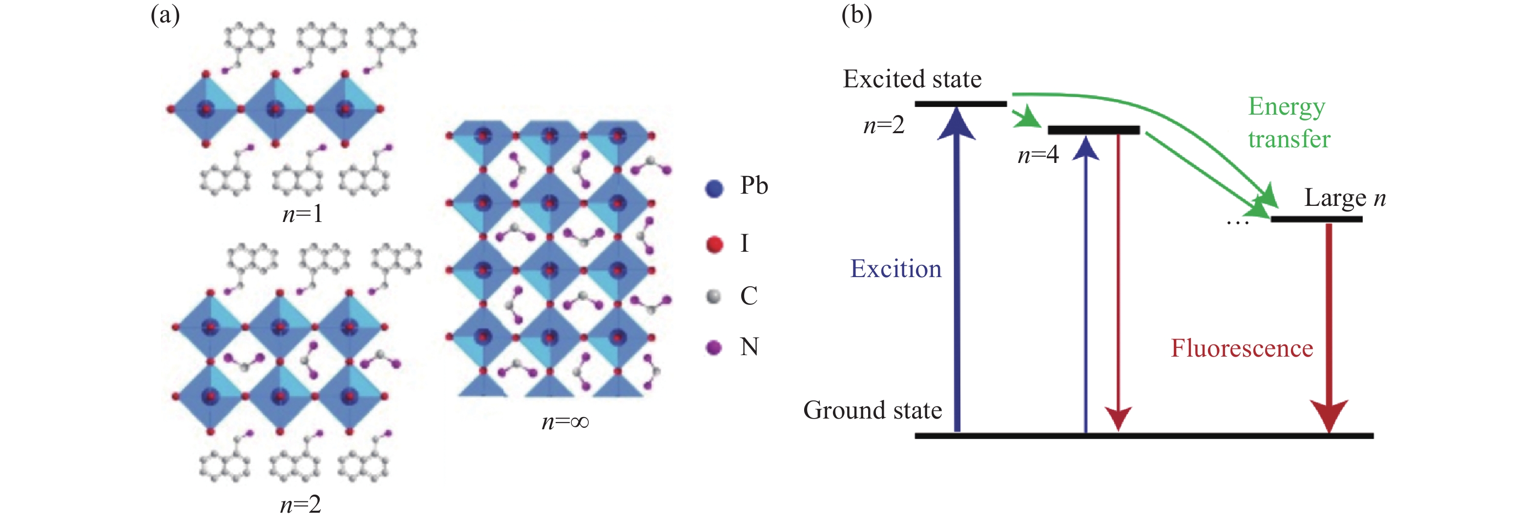
quasi-2D金属卤化物钙钛矿结构的通式是(A')m(A")n−1BnX3n+1(n=1,2,···),其中,(A')是大的有机长链间隔的阳离子(例如:2-苯乙胺(PEA+)和n-丁基铵(n-BA+)等,(A")是一价金属或有机短链阳离子(例如:Cs+、MA+、FA+等),B是二价金属阳离子,X是卤化物阴离子,n表示每个量子阱内[BX6]4−八面体层的数量。当n=1时,是2D钙钛矿;随着八面体数量增加至n=∞时,其钙钛矿的晶体结构和物理性质则与3D钙钛矿相近;而当n值具有1<n<∞的混合值时,为quasi-2D钙钛矿结构[29-31],见图2(a)。这是由于quasi-2D钙钛矿发光材料相较于3D钙钛矿结构,不同n结晶相被疏水性较强的有机长链离子环绕,可避免[BX6]4−正八面体与外界直接接触,具有更高的空气稳定性;其原位多量子阱结构的形成更有利于超快的能量漏斗效应[32]和电荷转移[33],可以增强激子的发光效率;quasi-2D钙钛矿晶粒受生长尺寸的限制,晶粒比3D钙钛矿小,且更致密,孔洞更少,漏电流现象也得到抑制。自2016年首次报道以quasi-2D钙钛矿材料作为发光光源制备PeLEDs以来,短短的几年里,quasi-2D PeLEDs的最大EQE值已飙升至30.84%[25]。这一系列的优势使得quasi-2D钙钛矿材料在电子和光学领域具有良好的应用前景。笔者后期研究也正是围绕quasi-2D钙钛矿材料(绿光PEA2Csn−1PbnBr3n+1和蓝光p-F-PEA2Csn−1PbnBr3n+1)展开的。
-
激子是由从PeLEDs的阳极和阴极分别注入的空穴和电子在空穴传输层/发光层界面、电子传输层/发光层界面相遇形成或在钙钛矿发光材料内部相遇形成的“电子-空穴”对。激子由25%的单重态激子和75%的三重态激子组成。在PeLEDs中,常引入具有荧光发光性能的有机小分子半导体传输材料(TPBi)、有机聚合物空穴传输材料(PVK)或传统聚合物荧光材料(PEO[34])等作为钙钛矿发光薄膜的添加剂或近邻层。这些材料中的激子在退激发时,由于自旋“禁阻”,以及单重态和三重态能级差较大,只有单重态激子可以通过发光辐射的形式退激发,而三重态激子不能以发光的形式退激发,导致四分之三的激子被浪费。这就使得用传统荧光材料作为掺杂剂或者界面缓冲层的 PeLEDs 的内量子效率(InternalQuantum Efficiency, IQE)不会超过25%。
为了使单重态激子的利用率更高和回收利用三重态激子能量,笔者在PeLEDs中引入不同种类的发光材料,使PeLEDs中IQE有望达到100%。
-
2017年,为了降低成本,笔者采用具有高电子迁移率和低成本的有机小分子传输材料Alq3作电子传输层,但导致钙钛矿发光层中的激子向紧邻的传输层扩散。为了解决该问题,在钙钛矿发光薄膜/Alq3界面引入了具有传统荧光发光性能的、能隙比TPBi、BAlq和Alq3都大的TmPyPB作激子阻挡层,有效地阻止了单重态激子的扩散。同时,如图3所示,深的HOMO能级能很好地将空穴限制在钙钛矿发光层中,进一步提高器件的激子复合效率。基于TmPyPB的绿光PeLEDs表现出最大的电流效率为9.37 cd/A,是没有激子阻挡层的对比器件的25倍[13]。
-
笔者采用结构优化法,将钙钛矿发光薄膜/传统有机小分子荧光材料单元(CsPbBr3/TmPyPB)多次旋涂制作如图4所示的(CsPbBr3/TmPyPB)n多量子阱结构,其中n=1或4。在具有4个单元的绿光PeLEDs中,激子产生界面比只有1个单元的多6个,激子的形成区域加宽,继而使激子产生界面处的激子浓度降低,减少激-激淬灭,使更多的激子辐射复合发光,改善了器件的EL性能和稳定性[14]。

图 4 激子产生的界面和区域示意图。(a)对比PeLEDs (n=1);(b)优化PeLEDs (n=4)。黑色实线代表产生激子的界面,红色虚线框代表产生激子的区域[14]
Figure 4. Schematic of interface and region of exciton generating for (a) PeLEDs (n=1); (b) Optimized PeLEDs (n=4). Black solid line represents the interface for exciton generation, and red dashed box represents the region for exciton generation[14]
-
在PEDOT: PSS/CsPbBr3之间引入一层具有传统荧光发光性能的空穴传输材料TAPC薄膜,如图5所示。TAPC可以有效地将PEDOT: PSS和CsPbBr3进行空间隔离,减少强酸性PEDOT: PSS对钙钛矿中激子的淬灭;由于TAPC具有高的LUMO能级,可以很好地将电子限制在钙钛矿发光层;同时,阶梯状的HOMO能级排布使空穴注入势垒降低,空穴传输能力得到明显提高,使钙钛矿中可以形成更多的激子;由于TAPC具有比钙钛矿大得多的能隙,激子能更好地限制在钙钛矿发光层中辐射发光。见图6,PEDOT: PSS/CsPbBr3界面处激子淬灭被有效抑制,获得了色纯度高、发光颜色稳定的绿光PeLEDs,最大发光亮度和电流效率分别是13198 cd/m2和6.84 cd/A[15]。

-
为了突破传统荧光材料中的强自旋轨道耦合的IQE(<25%)限制,在OLEDs领域里研究者们通常在有机小分子中引入重金属元素(如Ir等),使单重态激子上的能量可以通过系间窜越(Intersystem Crossing, ISC)传递到三重态激子上,继而退激,发出磷光,使IQE达到100%。笔者实验发现,在PeLEDs中引入有机磷光材料FIrpic有望提高单重态和三重态激子的利用率,使其IQE趋于100%。
-
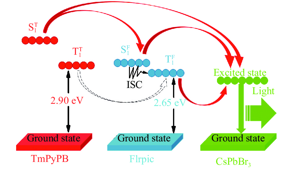
为了回收利用PeLEDs中的三重态激子,FIrpic被掺杂到CsPbBr3钙钛矿发光层中作为添加剂。有机磷光材料(FIrpic)的IQE接近100%,通常被用作OLEDs的蓝光光源,其三重态激子的能量(2.62 eV)远大于绿光钙钛矿发光材料CsPbBr3(2.37 eV),可以很好地将三重态激子限制在CsPbBr3中。如图7所示,FIrpic产生的激子中有25%是单重态激子,75%是三重态激子。一方面,能量通过ISC过程由FIrpic的单重态激子转移到FIrpic三重态激子;另一方面,能量可以通过Förster进行能量转移(蓝色箭头所示),由FIrpic单重态激子和FIrpic三重态激子转移到CsPbBr3激发态,使基于CsPbBr3: FIrpic发光层的绿光PeLEDs中单重态和三重态激子都可以得到有效利用[16]。
-
上述绿光PeLEDs中,在钙钛矿发光层中引入FIrpic 作添加剂,可以从一定程度上阻止三重态激子的扩散,但是PeLEDs中载流子传输不平衡,导致激子和载流子之间发生俄歇复合,激子的能量以热量的形式耗散。而笔者课题组在2017 年将电子传输材料TmPyPB引入钙钛矿发光薄膜中作为添加剂,表明TmPyPB的引入可以使载流子传输更平衡,同时还能提高钙钛矿薄膜的成膜质量,使得PeLEDs电致发光性能更好[35]。为了同时解决三重态激子利用率和载流子传输不平衡的问题,有机磷光材料FIrpic和电子传输材料TmPyPB作为复合添加剂同时引入到钙钛矿薄膜中。研究表明,同时引入FIrpic和TmPyPB不仅可以使钙钛矿薄膜更平整致密、全膜覆盖、缺陷降低,FIrpic还可以作激子能量在TmPyPB 与CsPbBr3之间转移的敏化剂。首先,在TmPyPB上形成单重态激子和三重态激子。见图8,能量通过Förster能量转移过程和Dexter能量转移过程分别由TmPyPB单重态激子和三重态激子上转移给FIrpic的单重态激子和三重态激子。同时,能量通过ISC过程由FIrpic单重态激子转移到FIrpic三重态激子能级。然后,能量通过Förster能量转移过程由TmPyPB的单重态激子、FIrpic单重态激子和FIrpic的三重态激子转移给CsPbBr3,形成激发态。最后,由CsPbBr3激发态退激辐射,发射绿光。最终,基于TmPyPB: FIrpic: CsPbBr3 复合薄膜作为发光层的PeLEDs实现了最大亮度、最大电流效率和最大 EQE 分别为37 784 cd/m2、22.6 cd/A和5.85%的高性能发光[17]。
-
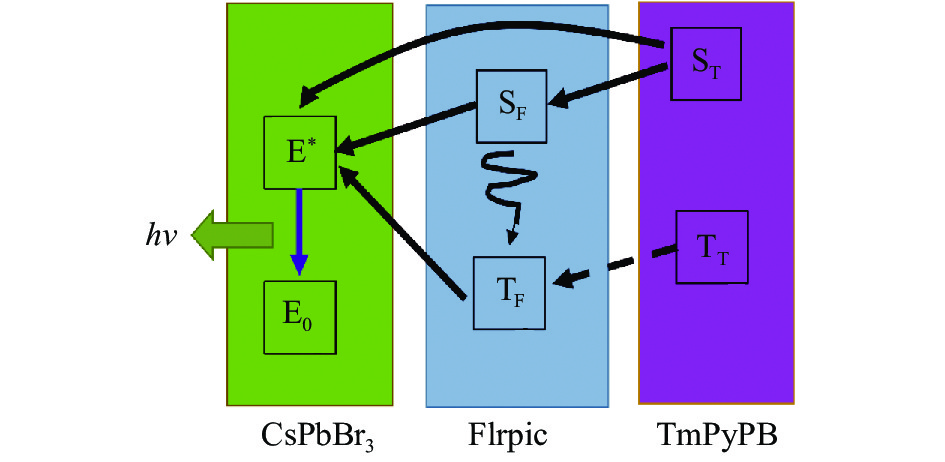
如前所述,笔者在PeLEDs中使用具有传统荧光发光性能的电荷传输材料作激子阻挡层(如TAPC、TmPyPB),虽然可以在 一定程度上抑制单重激子和三重态激子的扩散,但是这些材料由于自旋禁阻效应,其本身的三重态激子无法通过辐射复合的方式退激发,使得钙钛矿发光层中的三重态激子不能被充分利用来发光。为了解决这个问题,具有IQE接近100%的磷光材料FIrpic和具有电子传输能力的TmPyPB以共蒸的形式热蒸镀沉积到钙钛矿发光层(CsPbBr3)和电子传输层之间。如图9所示,CsPbBr3/TmPyPB: FIrpic 界面产生的所有激子都可以利用FIrpic作为磷光敏化剂,是主体材料TmPyPB的受体;是发光材料 CsPbBr3 的施主,其能量传递有两个途径,分别为:
$$ \begin{split} &{\rm S_T^*+S_F \rightarrow \mathrm{S}_T+S_F^*} \\ & {\rm S_F^* \rightarrow \mathrm{T}_F^*} \\ & \mathrm{~T}_{\rm F^*}+{\rm E_0 \rightarrow \mathrm{S}_F+E^*} \\ & {\rm E^* \rightarrow \mathrm{E}_0+}h v \end{split}$$ (1) $$ \begin{split} &{\rm T_T^*+S_F \rightarrow \mathrm{T}_T+T_F^* }\\ &{\rm T_F^*+E_0 \rightarrow S_F+E^*} \\ &{\rm E^* \rightarrow \mathrm{E}_0}+h v \end{split}$$ (2) 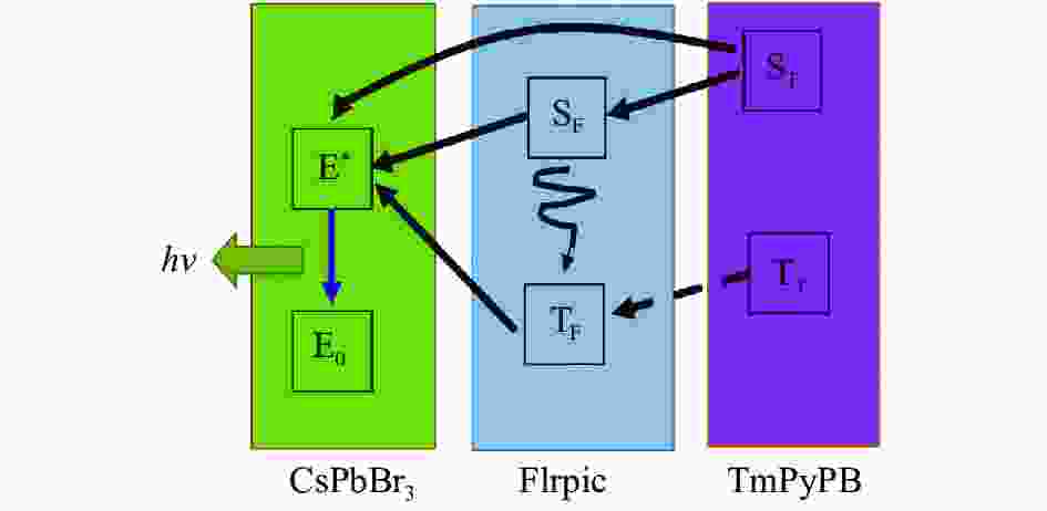
图 9 CsPbBr3发光层和TmPyPB: FIrpic复合激子阻挡层之间的多级能量转移示意图(虚线箭头表示 Dexter能量转移,实线箭头表示Förster 能量转移)[18]
Figure 9. Schematic of energy transfer processes between the CsPbBr3 emission layer and the TmPyPB: FIrpic composite exciton blocking layer(dashed arrows indicate Dexter energy transfer and solid arrows indicate Förster energy transfer)[18]
式中:hv为发出光子的能量;S和T分别表示单重态激子和三重态激子;下脚标T和F分别表示所用的主体材料TmPyPB 和染料敏化剂 FIrpic;E0 和 E*分别表示钙钛矿发光材料CsPbBr3 的基态和激发态;上角标*表示激发态。最终,基于TmPyPB: FIrpic复合激子阻挡层的PeLEDs的电致发光效率和稳定性都比参考器件提高了2倍多[18]。
-
有机磷光材料中,稀有金属元素(如Ir或Pt,Re等)的引入使成本增加。为解决这个问题并突破自旋禁阻效应,实现100%的IQE,Adachi课题组在2012年提出并获得了无需引入重金属元素的、IQE接近100%的热激活延迟荧光(TADF)材料。与传统的荧光材料相比,TADF的单重态激子(S1)能级和三重态激子能级(T1)的能极差小很多(小于100 meV),使得能量可以通过反向系间窜越过程(Reverse Intersystem Cross-ing, RISC)由三重态激子转移到单重态激子上,然后辐射复合发出荧光,实现100%的激子利用率。下面将讨论将不同种类的TADF分子(分子结构如图10所示)引入PeLEDs中的能量转移机理。
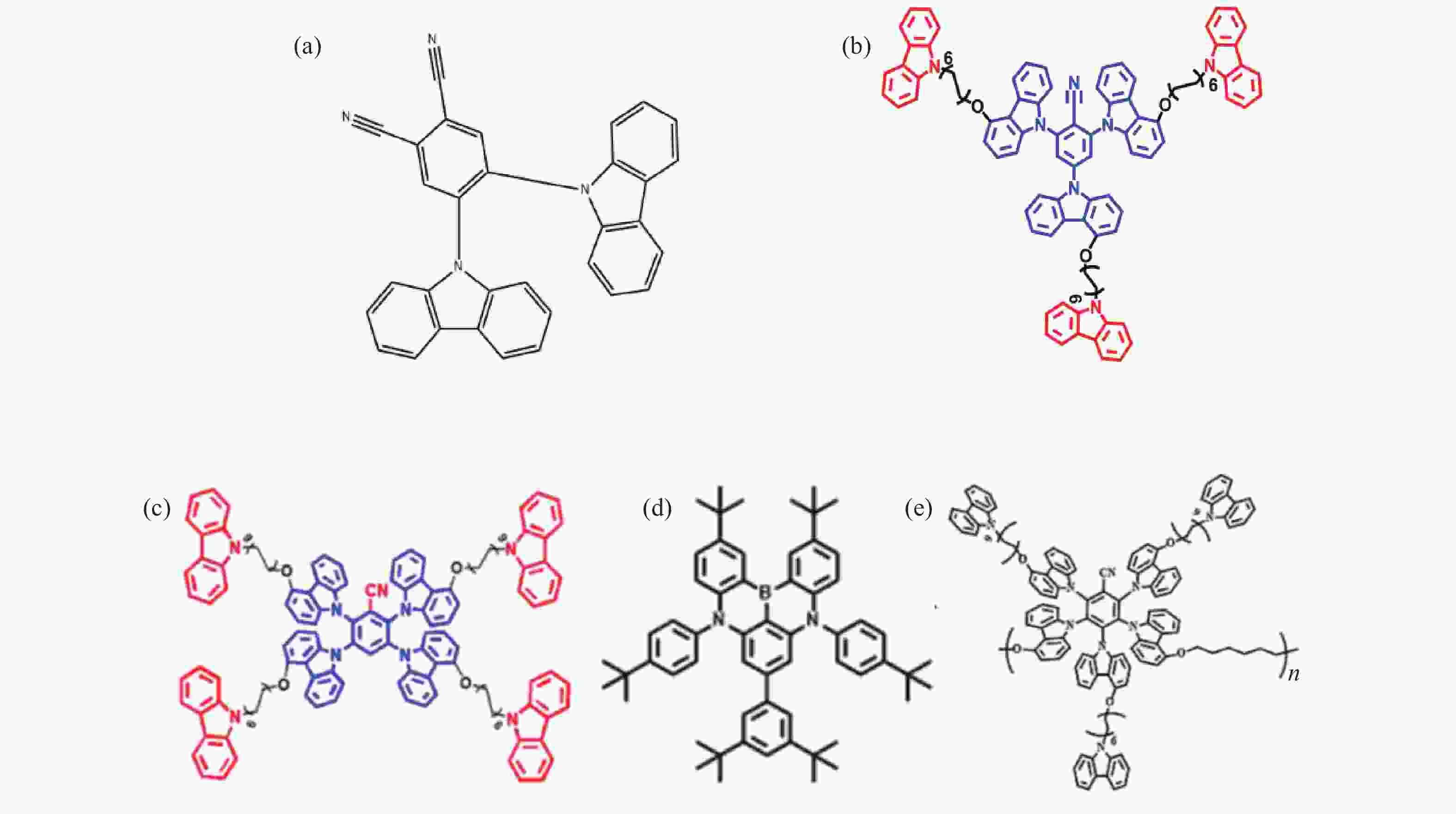
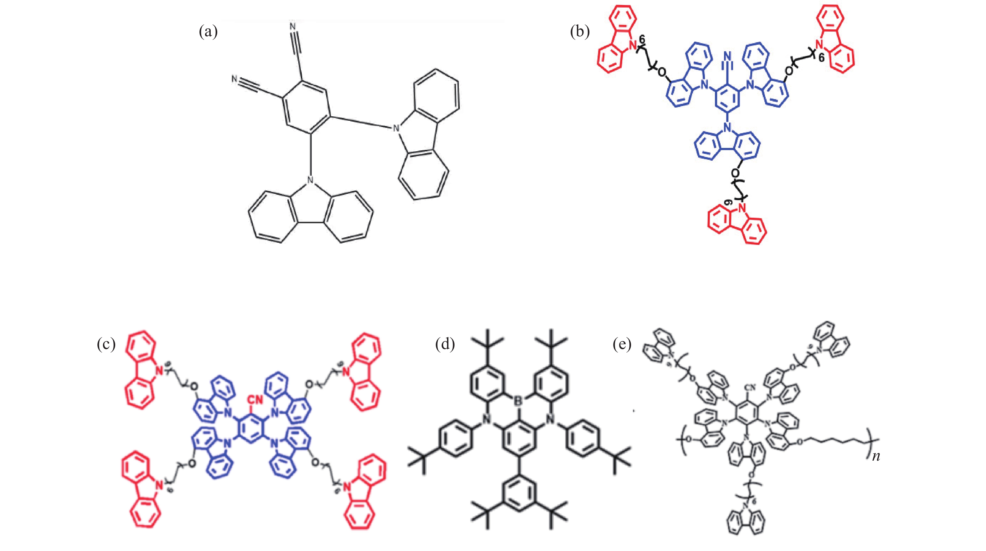
图 10 热激活延迟荧光材料(TADF)的分子结构。(a) 2CzPN (传统TADF);(b) Cz-3CzCN (TADF 树形分子);(c) Cz-4CzCN (TADF 树形分子);(d) t-DABNA-dtB(TADF 树形分子);(e) P-Cz5CzCN (TADF 聚合物)[19-24]
Figure 10. Molecular structure of thermally activated delayed fluorescence materials (TADF). (a) 2CzPN (traditional TADF); (b) Cz-3CzCN (TADF dendrimer); (c) Cz-4CzCN (TADF dendrimer); (d) t-DABNA-dtB (TADF dendrimer); (e) P-Cz5CzCN (TADF polymer)[19-24]
-
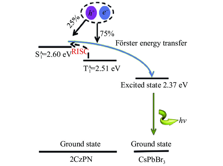
基于传统的TADF材料2CzPN(分子结构如图10(a)所示)作添加剂的PeLEDs中CsPbBr3: 2CzPN混合发光薄膜的能量转移示意图见图11。单重态(${\rm S}_{1}^{\rm A}$)、三重态(${\rm T}_{1}^{\rm A}$)激子在2CzPN上形成后,由于它们之间的能极差很小(约0.09 eV),三重态激子上的能量可以通过RISC上转换到更高的单重态激子能级上。然后,2CzPN单重态激子上的能量通过Fӧrster能量转移过程转移到CsPbBr3的激发态上退激发出绿光,实现了潜在的100%IQE。最终,利用溶液一步旋涂方法,制备了基于CsPbBr3: 2CzPN的高性能绿光PeLEDs,启亮电压和最高亮度分别是3.6 V和22063 cd/m2[19]。
-
真空蒸镀的2CzPN超薄缓冲层被引入到CsPbBr3层和TmPyPB层之间,可以阻止CsPbBr3的激子向TmPyPB层扩散,起到荧光增敏剂的作用,将激子有效地限制在CsPbBr3,使得单重态和三重态激子的辐射发光效率更高,能量转移图如图11所示。由于2CzPN超薄缓冲层的存在,绿光PeLEDs的电致发光性能比参考器件显著提高[20]。
-
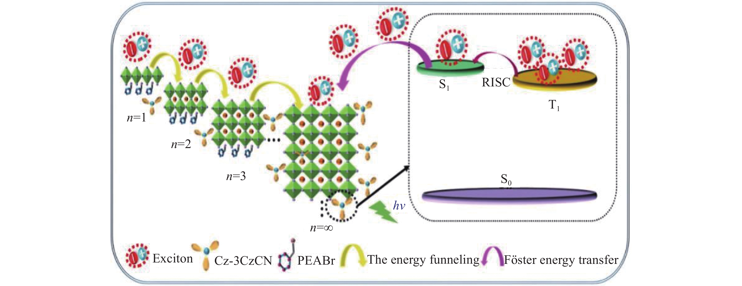
上述的传统TADF发光核(如2CzPN)末端没有被不发光的有机官能团封装,容易受到水和氧气的破环,并且激子浓度大时,容易发生分子聚集和激-激淬灭,不利于激子的有效利用,限制PeLEDs器件效率和稳定性的进一步提高。为了解决该问题,笔者采用班老师组合成的具有“核”-“壳”结构的TADF树形分子Cz-3CzCN和Cz-4CzCN(分子结构如图10(b)和(c)所示)作添加剂,可以进一步提高激子的利用率。Cz-3CzCN (Cz-4CzCN)是由一个3CzCN(4CzCN)TADF发光核和3个(4个)烷基链咔唑有机官能团作封装“壳”。由于封装“壳”的存在可以保护TADF发光“核”的光电性能不受环境的影响,同时使材料更易溶于常见有机溶剂,并抑制TADF发光核之间的分子间相互作用,减少分子聚集和由于激子浓度高带来的激-激淬灭,更高效地利用激子。图12展示了激子在PEA2Csn−1PbnBr3n+1和Cz-3CzCN上形成后,激子能量由于Cz-3CzCN围绕在钙钛矿晶粒四周,其能量可以被Cz-3CzCN限制在quasi-2D钙钛矿晶粒PEA2Csn−1PbnBr3n+1中的能量转移过程。一方面,在PEA2Csn−1PbnBr3n+1上形成的激子,能量通过能量漏斗效应从小n结晶相能级转移到大n结晶相能级,直至n=∞的三维钙钛矿相辐射发光。另一方面,在Cz-3CzCN上形成的激子,由于单重态激子和三重态激子之间的能量差很小,能量可以通过RISC过程从三重态激子转移到单重态上。然后,能量通过Förster能量转移由Cz-3CzCN单重态直接转移到大n(例如n=∞)上辐射发绿光。同时,由于Cz-3CzCN的钝化作用,PEA2Csn−1PbnBr3n+1薄膜的缺陷减少,颗粒更小,薄膜的形貌更好,更有利于激子辐射复合发光。最后,Cz-3CzCN(Cz-4CzCN)中的烷基链咔唑基团还能保护钙钛矿免受水和氧的侵蚀,避免发光“核”之间的直接接触,降低由分子聚集和激子浓度高带来激-激淬灭。因此,绿光quasi-2D PeLEDs的光电性能得到极大的提升,最大的电流效率达到39 cd/A,比不添加“核”-“壳”TADF的器件时提高了5倍[21-22]。
-
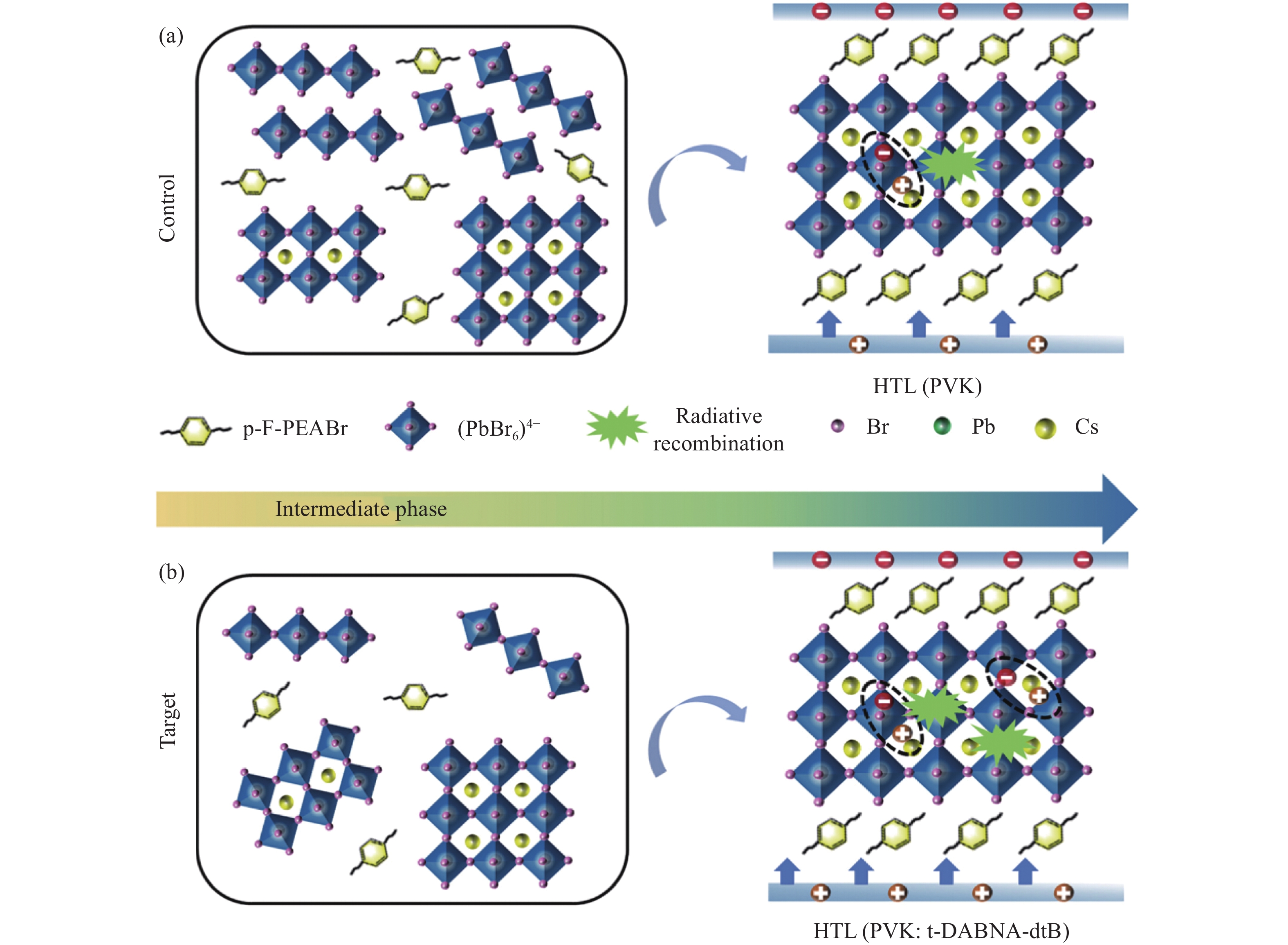
为解决激子向空穴传输层扩散的问题,笔者在聚合物空穴传输材料(PVK)中掺杂具有“核”-“壳”结构的TADF树形分子t-DABNA-dtB (分子结构见图10(d)),使准二维钙钛矿薄膜p-F-PEA2Csn−1PbnBr3n+1的缺陷态密度更低、成膜质量更好,空穴的注入和传输能力得到增强,可以使钙钛矿结晶相的分布更有利于能量漏斗效应的发生,最重要是t-DABNA-dtB分子可以作为染料敏化剂,利用Förster能量转移通道来回收利用钙钛矿发光层中扩散到空穴传输层的激子,提高蓝光PeLEDs的光电性能。图13所示为基于PVK: t-DABNA-dtB复合薄膜作荧光增强剂的蓝光quasi-2D PeLEDs中相位分布、载流子输运和激子辐射复合的示意图。优化的蓝光quasi-2D PeLEDs的亮度达到1599 cd/m2, EQE 达到12.38%,器件半寿命达到 1236 s[23]。
-
TADF树形分子可以很好地回收利用单重态激子和三重态激子,也可以很好地避免TADF分子发光核之间的激-激淬灭,但是TADF树形分子的导电性不好。为了解决导电性差的问题,笔者采用班老师组合成的两种聚合物作为钙钛矿发光薄膜的添加剂,即导电性差的无“TADF发光核”-“壳”结构的绝缘聚合物P-5CzCN和导电性较好的有“TADF发光核”-“壳”结构的半导体TADF聚合物P-Cz5CzCN。研究表明:两种聚合物都可以钝化钙钛矿膜的缺陷来减少钙钛矿的非辐射跃迁从而抑制俄歇复合,但是无“TADF发光核”-“壳”结构的绝缘体聚合物P-5CzCN不能有效地抑制激子的淬灭,而具有“TADF发光核”-“壳”结构的半导体聚合物P-Cz5CzCN更有利于改善载流子传输和改善激子利用率,如图14所示。进一步的研究表明:具有“TADF发光核”-“壳”结构的聚合物更有利于增强疏水性、钙钛矿的热稳定性、结晶的均匀性和发光性能。最后,基于有“TADF发光核”-“壳”结构的TADF聚合物的绿光quasi-2D PeLED实现了66.1 cd/A的高电流效率和17.4%的EQE,小的效率滚降和高的色纯度[24]。
-
文中总结了近5年来笔者课题组和班鑫鑫老师课题组、王照奎老师课题组为了增强激子限制和激子回收利用,在PeLEDs中引入不同种类的有机发光材料到钙钛矿发光层内作添加剂或者钙钛矿发光层/传输层界面作激子回收的敏化剂,或者多次旋涂制作多量子阱结构。研究表明:引入能隙比钙钛矿能隙更大的传统荧光发光材料可以更好地回收单重态激子;引入单重态和三重态激子能量都远高于钙钛矿能隙的、内量子效率接近100%的有机磷光材料和不同种类的TADF材料可以更好地回收利用单重态和三重态激子,使PeLED的IQE有望达到100%。与传统的TADF材料相比,新型TADF材料:具有“核”-“壳”结构的TADF树形分子(例如,Cz-3CzCN和Cz-4CzCN等)、具有“TADF核”-“壳”结构的半导体TADF聚合物(P-Cz5CzCN),可以钝化薄膜内的缺陷的同时,还可以有效地抑制TADF发光核之间由于直接接触所导致的激-激淬灭,进一步提高激子的利用率,使绿光和蓝光PeLEDs的效率和稳定性得到极大的提高。这种方法在基于3D的钙钛矿发光薄膜(CsPbBr3)和quasi-2D钙钛矿发光薄膜(PEA2Csn−1PbnBr3n+1、p-F-PEA2Csn−1PbnBr3n+1)的PeLEDs中得到了论证。该方法也可以应用其他类型的钙钛矿发光器件,以实现高效率和高稳定性,为钙钛矿发光器件的商业化提供一条可行的参考策略。
Research progress of high-performance PeLEDs based on organic light-emitting materials (invited)
-
摘要: 近年来,金属卤化物钙钛矿发光材料由于具有优异的光电性能,被广泛地应用于金属卤化物钙钛矿发光二极管(Perovskite light-emitting diodes, PeLEDs),被视作下一代显示和照明领域的发光光源。激子利用率是影响PeLEDs效率的关键因素之一,研究者采用各种各样的方法将激子限制在钙钛矿发光层中,对激子能量回收利用以提高激子的利用率。文中将概述通过添加剂辅助法、器件界面工程和结构优化法,将传统荧光材料、磷光材料、热激活延迟荧光材料引入器件,改善绿光和蓝光PeLEDs的光电性能方面所做的尝试。并简要地介绍激子限制作用的原理,以及不同类型的发光材料引入PeLEDs中激子的能量转移机理和器件光电性能提升的物理机理。
-
关键词:
- 金属卤化物钙钛矿发光二极管 /
- 激子利用率 /
- 磷光材料 /
- 热激活延迟荧光材料
Abstract:Objective In recent years, metal halide perovskite light-emitting materials have attracted great attention for their application in metal halide perovskite light-emitting diodes (PeLEDs) due to their outstanding optoelectronic properties, and are considered as the next generation of light-emitting sources in the field of display and lighting. Exciton utilization is one of the key factors affecting the efficiency of PeLEDs. Various methods have been employed to confine excitons in the perovskite light-emitting layer and recycle the energy of excitons to improve the utilization rate of excitons. This article will review the attempts made to improve the optoelectronic properties of green and blue PeLEDs by utilizing traditional fluorescent materials, phosphorescent materials, and thermally activated delayed fluorescent materials. It will also briefly introduce the principle of exciton confinement, as well as the energy transfer mechanism of different types of light-emitting materials introduced into green and blue PeLEDs and the physical mechanism of improving the optoelectronic properties. Methods Films are fabricated using the methods of spincoating and vacuum thermal evaporation deposition. All the perovskites films are obtained by spincoating method. Various types of organic luminescent materials are introduced into the perovskite emissive layer as additives or inserted between the perovskite emissive layer/transport layer as sensitizers for exciton recycling, or through multiple coating to create multi-quantum well structures. These materials are brought into the PeLEDs through additive-assisted methods, device interface engineering, and structural optimization methods. Results and Discussions It has been demonstrated that the introduction of traditional fluorescent emitters with a larger bandgap than that of the perovskite can better recycle singlet excitons. The incorporation of organic phosphorescent materials and different types of TADF materials, which have internal quantum efficiencies near 100% and energies of both singlet and triplet excitons that are significantly higher than the bandgap of the perovskites, can better recycle and utilize both singlet and triplet excitons of the perovskites. This leads to a potential internal quantum efficiency value of 100% for PeLEDs. Compared to traditional TADF materials, new TADF materials with a "core"-"shell" structure (such as Cz-3CzCN and Cz-4CzCN) and semiconductor TADF polymers with a "TADF core"-"shell" structure (such as P-Cz5CzCN) can not only passivate the defects in the perovskites film but also effectively suppress "exiton"-"exiton" quenching due to direct contact between the TADF emission cores. This further improves the utilization of excitons, greatly enhancing the efficiency and stability of green- and blue-emitting PeLEDs. Conclusions This article reviews the work made by the groups of Gao Chunhong, Ban Xinxin and Wang Zhaokui in the fields of exciton confinement and exciton recycling in the past five years. These approaches mentioned above have been demonstrated in PeLEDs based on 3D perovskite emissive films (CsPbBr3) and quasi-2D perovskite emissive films (PEA2Csn-1PbnBr3n+1, p-F-PEA2Csn-1PbnBr3n+1). These methods can also be extended to various types of light-emitting devices to achieve efficient and stable PeLEDs, providing a feasible strategy for the commercialization of PeLEDs. -
图 1 ABX3 金属卤化物钙钛矿的一般晶体结构。 (a) A阳离子占据晶格角,B阳离子占据间隙位,X阴离子占据晶格面心;(b)另一种视角下,B阳离子聚集在X阴离子周围形成[BX6]4−结构[27-28]
Figure 1. ABX3 metal halide perovskite general crystal structure. (a) A-type cations occupy lattice corners, B-type cations occupy interstitial sites, and X-type anions occupy lattice face centers; (b) B-type cations cluster around X-type anions to form [BX6]4− structures[27-28]

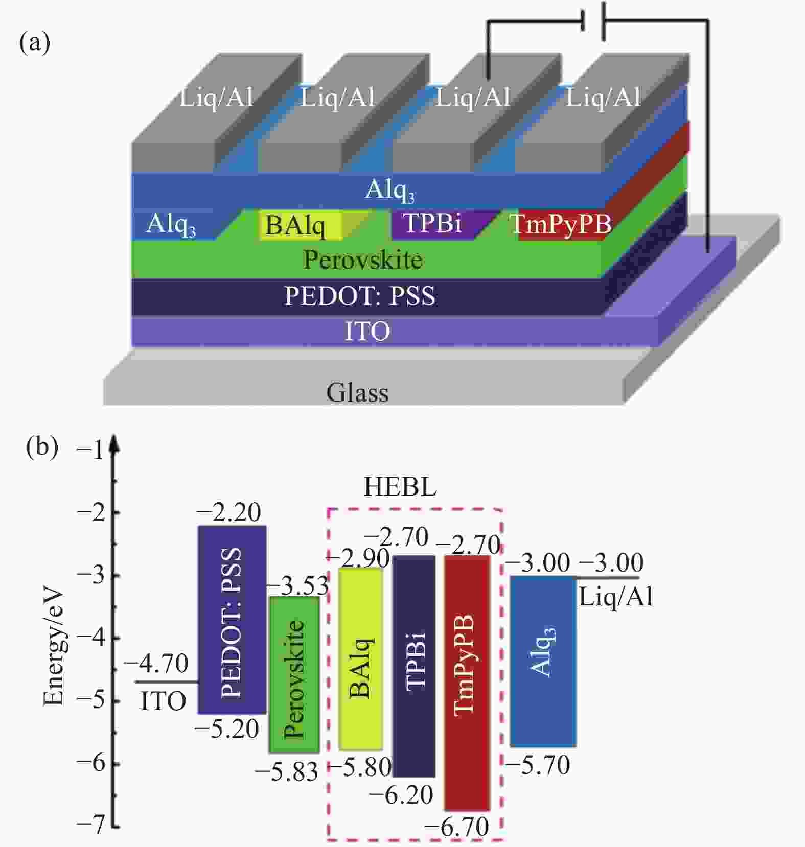
图 4 激子产生的界面和区域示意图。(a)对比PeLEDs (n=1);(b)优化PeLEDs (n=4)。黑色实线代表产生激子的界面,红色虚线框代表产生激子的区域[14]
Figure 4. Schematic of interface and region of exciton generating for (a) PeLEDs (n=1); (b) Optimized PeLEDs (n=4). Black solid line represents the interface for exciton generation, and red dashed box represents the region for exciton generation[14]
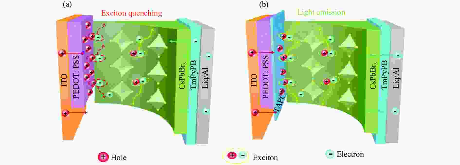


图 9 CsPbBr3发光层和TmPyPB: FIrpic复合激子阻挡层之间的多级能量转移示意图(虚线箭头表示 Dexter能量转移,实线箭头表示Förster 能量转移)[18]
Figure 9. Schematic of energy transfer processes between the CsPbBr3 emission layer and the TmPyPB: FIrpic composite exciton blocking layer(dashed arrows indicate Dexter energy transfer and solid arrows indicate Förster energy transfer)[18]
图 10 热激活延迟荧光材料(TADF)的分子结构。(a) 2CzPN (传统TADF);(b) Cz-3CzCN (TADF 树形分子);(c) Cz-4CzCN (TADF 树形分子);(d) t-DABNA-dtB(TADF 树形分子);(e) P-Cz5CzCN (TADF 聚合物)[19-24]
Figure 10. Molecular structure of thermally activated delayed fluorescence materials (TADF). (a) 2CzPN (traditional TADF); (b) Cz-3CzCN (TADF dendrimer); (c) Cz-4CzCN (TADF dendrimer); (d) t-DABNA-dtB (TADF dendrimer); (e) P-Cz5CzCN (TADF polymer)[19-24]


-
[1] Era M, Morimoto S, Tsutsui T, et al. Organic-inorganic hetero-structure electroluminescent device using a layered perovskite semiconductor (C6H5C2H4NH3)2PbI4 [J]. Applied Physics Letters, 1994, 65(6): 676-678. doi: 10.1063/1.112265 [2] Tan Z K, Moghaddam R S, Lai M L, et al. Bright light-emitting diodes based on organometal halide perovskite [J]. Nature Nanotechnology, 2014, 9(9): 687-692. doi: 10.1038/nnano.2014.149 [3] Shen X, Kang K, Yu Z, et al. Passivation strategies for mitigating defect challenges in halide perovskite light-emitting diodes [J]. Joule, 2023, 7(2): 272-308. doi: 10.1016/j.joule.2023.01.008 [4] Fakharuddin A, Gangishetty M K, Abdi-jalebi M, et al. Perovskite light-emitting diodes [J]. Nature Electronics, 2022, 5(4): 203-216. doi: 10.1038/s41928-022-00745-7 [5] Yan C, Lin K, Lu J, et al. Composition engineering to obtain efficient hybrid perovskite light-emitting diodes [J]. Frontiers of Optoelectronics, 2020, 13(3): 282-290. doi: 10.1007/s12200-020-1046-7 [6] Zhang L, Li N, Liu D, et al. Deep learning for additive screening in perovskite light-emitting diodes [J]. Angewandte Chemie International Edition, 2022, 61(37): e202209337. doi: 10.1002/anie.202209337 [7] Shan Q, Song J, Zou Y, et al. High performance metal halide perovskite light-emitting diode: from material design to device optimization [J]. Small, 2017, 13(45): 1701770. doi: 10.1002/smll.201701770 [8] Han T, Tan S, Xue J, et al. Interface and defect engineering for metal halide perovskite optoelectronic devices [J]. Advanced Materials, 2019, 31(47): 1803515. doi: 10.1002/adma.201803515 [9] Saleem M I, Choi R, Lee J H. Light outcoupling strategies in oriented perovskite light-emitting-diodes: recent trends, opportunities, and challenges toward innovation [J]. Materials Chemistry Frontiers, 2023, 7(12): 2316-2336. doi: 10.1039/D2QM01365G [10] Xia Y, Lou Y H, Zhou Y H, et al. Solvent strategies toward high-performance perovskite light-emitting diodes [J]. Journal of Materials Chemistry C, 2022, 10(9): 3276-3286. doi: 10.1039/D1TC05685A [11] Chen H, Fan L, Zhang R, et al. Sodium ion modifying in situ fabricated CsPbBr3 nanoparticles for efficient perovskite light emitting diodes [J]. Advanced Optical Materials, 2019, 7(21): 1900747. doi: 10.1002/adom.201900747 [12] Liu Y, Ono L K, Qi Y. Organic additive engineering toward efficient perovskite light-emitting diodes [J]. InfoMat, 2020, 2(6): 1095-1108. doi: 10.1002/inf2.12098 [13] Wang R, Zhang Y, Yu F, et al. An efficient CsPbBr3 perovskite light-emitting diode by employing 1, 3, 5-tri(m-pyrid-3-yl-phenyl)benzene as a hole and exciton blocking layer [J]. Journal of Luminescence, 2020, 219: 116915. doi: https://doi.org/10.1016/j.jlumin.2019.116915 [14] Wang R, Jia Y L, Ding L, et al. Efficient halide perovskite light-emitting diodes with emissive layer consisted of multilayer coatings [J]. Journal of Applied Physics, 2019, 126(16): 165502. doi: 10.1063/1.5110523 [15] Wang Run, Jia Yalan, Zhang Yue, et al. High efficiency green perovskite light-emitting diodes based on exciton blocking layer [J]. Acta Physica Sinica, 2020, 69(3): 038501. (in Chinese) doi: 10.7498/aps.69.20191263 [16] Gao C H, Ma X J, Zhang Y, et al. 84% efficiency improvement in all-inorganic perovskite light-emitting diodes assisted by a phosphorescent material [J]. RSC Advances, 2018, 8(28): 15698-15702. doi: 10.1039/C7RA13231J [17] Gao C H, Yu F X, Xiong Z Y, et al. 47-Fold EQE improvement in CsPbBr3 perovskite light-emitting diodes via double-additives assistance [J]. Organic Electronics, 2019, 70: 264-271. doi: https://doi.org/10.1016/j.orgel.2019.04.018 [18] Gao C, Xiong Z, He Z, et al. Boosting the external quantum efficiency in perovskite light-emitting diodes by an exciton retrieving layer [J]. Journal of Materials Chemistry C, 2019, 7(28): 8705-8711. doi: 10.1039/C9TC02258A [19] Gao C H, Zhang Y, Ma X J, et al. A method towards 100% internal quantum efficiency for all-inorganic cesium halide perovskite light-emitting diodes [J]. Organic Electronics, 2018, 58: 88-93. doi: https://doi.org/10.1016/j.orgel.2018.04.007 [20] Jia Y L, Wang R, Zhang Y, et al. Large current efficiency enhancement in the CsPbBr3 perovskite light-emitting diodes assisted by an ultrathin buffer layer [J]. Journal of Luminescence, 2019, 209: 251-257. doi: https://doi.org/10.1016/j.jlumin.2019.01.056 [21] Ban X, Yu J, He X, et al. Highly efficient quasi-2D perovskite light-emitting diodes incorporating a TADF dendrimer as an exciton-retrieving additive [J]. ACS Applied Materials & Interfaces, 2021, 13(37): 44585-44595. doi: 10.1021/acsami.1c14493 [22] He X, Qiu S, Xu Q, et al. Exciton harvesting in quasi-2D perovskite light-emitting diodes with an encapsulated thermally activated delayed fluorescence [J]. Applied Physics Letters, 2021, 119(24): 242101. doi: 10.1063/5.0071335 [23] Yang W, Gao C H, Xia Y, et al. Enhancing energy channel and carriers recycling in sky-blue perovskite light-emitting diodes via a fluorescent fortifier [J]. Applied Physics Letters, 2023, 123(15): 153502. doi: 10.1063/5.0172757 [24] Ban X, Cao Q, Yang W, et al. Developing TADF polymer as semiconductor additive for high performance perovskite light emitting diodes with dual recombination channel and small efficiency roll-off [J]. Chemical Engineering Journal, 2023, 474: 145749. doi: https://doi.org/10.1016/j.cej.2023.145749 [25] Bai W, Xuan T, Zhao H, et al. Perovskite light-emitting diodes with an external quantum efficiency exceeding 30% [J]. Advanced Materials, 2023, 35(39): 2302283. doi: 10.1002/adma.202302283 [26] Rose G. Ueber einige neue mineralien des urals [J]. Journal für Praktische Chemie, 1840, 19(1): 459-468. doi: https://doi.org/10.1002/prac.18400190179 [27] Wei Z, Xing J. The rise of perovskite light-emitting diodes [J]. The Journal of Physical Chemistry Letters, 2019, 10(11): 3035-3042. doi: 10.1021/acs.jpclett.9b00277 [28] Chen Q, De Marco N, Yang Y (Michael), et al. Under the spot-light: the organic-inorganic hybrid halide perovskite for optoelectronic applications [J]. Nano Today, 2015, 10(3): 355-396. doi: 10.1016/j.nantod.2015.04.009 [29] Lan C, Zhou Z, Wei R, et al. Two-dimensional perovskite materials: from synthesis to energy-related applications [J]. Materials Today Energy, 2019, 11: 61-82. doi: https://doi.org/10.1016/j.mtener.2018.10.008 [30] Chen Y, Sun Y, Peng J, et al. 2D ruddlesden-popper perovskites for optoelectronics [J]. Advanced Materials, 2018, 30(2): 1703487. doi: 10.1002/adma.201703487 [31] Gao X, Zhang X, Yin W, et al. Ruddlesden-popper perovskites: synthesis and optical properties for optoelectronic applications [J]. Advanced Science, 2019, 6(22): 1900941. doi: 10.1002/advs.201900941 [32] Wang N, Cheng L, Ge R, et al. Perovskite light-emitting diodes based on solution-processed self-organized multiple quantum wells [J]. Nature Photonics, 2016, 10(11): 699-704. doi: 10.1038/nphoton.2016.185 [33] Chen P, Meng Y, Ahmadi M, et al. Charge-transfer versus energy-transfer in quasi-2D perovskite light-emitting diodes [J]. Nano Energy, 2018, 50: 615-622. doi: https://doi.org/10.1016/j.nanoen.2018.06.008 [34] Bade S, Shan X, Hoang P, et al. Stretchable light-emitting diodes with organometal-halide-perovskite–polymer composite emitters [J]. Advanced Materials, 2017, 29(23): 1607053. doi: https://doi.org/10.1002/adma.201607053 [35] Yu F X, Zhang Y, Xiong Z Y, et al. Full coverage all-inorganic cesium lead halide perovskite film for high-efficiency light-emitting diodes assisted by 1, 3, 5-tri(m-pyrid-3-yl-phenyl)ben-zene [J]. Organic Electronics, 2017, 50: 480-484. doi: https://doi.org/10.1016/j.orgel.2017.08.026 -

 点击查看大图
计量
- 文章访问数: 159
- HTML全文浏览量: 71
- PDF下载量: 57
- 被引次数: 0

