


 下载:
下载:


-
光电探测器是一种利用光电效应将光信号转化为电信号的传感器。它们在可穿戴设备、光通信系统、环境传感器等各种应用中引起了学界极大地研究兴趣[1−4]。
随着光电探测器向着低维度、多波段、可调节的方向发展,金属氧化物由于其可调谐的带隙、较高的载流子迁移率和较大的比表面积而受到广泛关注。其中,ZnO作为宽带隙氧化物半导体(室温下禁带宽度Eg = 3.37 eV),对紫外光具有良好的响应[5−6]。然而,ZnO存在两个问题:一是光诱导电子-空穴对的快速复合,导致光电转换效率较差;二是ZnO的紫外光谱响应只占太阳光谱的5%左右,限制了其对可见光区域的利用。
目前,构建异质结是拓宽氧化物半导体对太阳光谱利用范围的常用方法。窄带隙半导体具备长波长光谱吸收能力,宽带隙半导体具备短波长光谱吸收能力,选用合适的半导体材料构建异质结,可以丰富异质结界面能带结构的可调性,相比于单一的半导体,其光谱响应范围更宽[7−11]。同时,异质结中的内建电场可加快光生电子和空穴的有效分离,有利于提升光电子器件的载流子输运特性。基于上述原因,异质结常被用于光电探测器的制备研究[12−14]。
金属硒化物因其高化学稳定性以及优异的光学和电学性能而被广泛应用于光电子领域。ZnSe是一种n型直接带隙半导体,禁带宽度Eg= 2.7 eV,是与一维氧化锌纳米线结合形成异质结构的理想材料。ZnSe与ZnO可形成II型异质结,不仅能促进载流子分离,调控界面的电子输运特性,还可以提高低维光电材料对可见光的吸收。M. Ghoul等人[15]利用两步电化学沉积法生长了ZnO/ZnSe核壳纳米线,其ZnSe壳层显著抑制了ZnO/ZnSe纳米结构中光生电子-空穴对的复合速率,提高了响应光电流。同时,紫外-可见光谱测量结果证实ZnO/ZnSe纳米结构增强了器件对可见光波段的吸收。此外,Wang等人[14]通过阴离子交换法用Se2-原位取代氧化锌纳米片中O2-并成功制备了过渡区较窄的ZnO/ZnSe/Au纳米复合材料,其光电流约为0.158 mA/cm2,大约是Au/ZnO光电流的两倍。相比于ZnO/Au的载流子寿命(46.82 s),ZnO/ZnSe/Au纳米复合材料的载流子寿命(126.26 s)有所增加,原因是原位取代形成的异质结可以有效地降低界面转移电阻,增加载流子寿命。
除构建低维异质结外,贵金属表面沉积、表面敏化、0 D量子点修饰、金属离子掺杂等方法也常用于提升光电探测器的响应范围和探测灵敏度。基于表面等离子体共振效应,贵金属零维纳米颗粒对光具有很好的局域能力,能有效提高材料的光吸收。相比于其他贵金属纳米颗粒,比如金纳米颗粒,银(Ag)纳米颗粒性价比更高,而其他常见的铝、铜等纳米颗粒制备困难且稳定性较差,难以应用于实际。
文中描述了一种等离子体增强型异质结阵列光电探测器的制备,其中氧化锌纳米线和硒化锌异质结构作为一种光敏材料,结合银纳米颗粒产生表面等离子共振效应,增强器件对光的吸收。本工作采用低温水热法、化学气相沉积法在FTO衬底上合成一维ZnO纳米线与ZnSe壳层异质结,然后通过毛细管自组装法将银纳米颗粒均匀沉积在异质结上,制备了等离子体增强型异质结阵列光电探测器件。该技术制备简单且成本低,不涉及昂贵工艺。利用扫描电子显微镜(SEM)、X射线衍射(XRD)、拉曼光谱和紫外-可见光谱等各种技术,对硒化锌和氧化锌的表面形貌、相组成、光学性质、光电性能进行了表征。研究发现,该器件具有良好的响应度、响应时间及稳定性,为制备出光电转换效率更高的光电探测器提供了实际的参考策略,可应用于新型军用快速光电探测器、物质分析检测器、生物传感器等领域。
-
制备过程通过以下3个步骤进行(制备工艺流程如图1所示):1) 水热法生长ZnO纳米线阵列。在干净的FTO衬底上旋涂5 mmol/L的醋酸锌溶液作为籽晶层,然后将其置于0.05 mmol/L的六水合硝酸锌溶液与六次甲基四胺溶液混合的前驱体溶液中,通过水热法反应3~4 h,重复生长过程得到目标长度的ZnO纳米线;2) 化学气相沉积法合成一维ZnO/ZnSe异质结阵列。将ZnO纳米线与Se粉分别置于化学气相沉积反应炉,反应温度分别设置为400 ℃和270 ℃,在Ar∶H2 配比为95∶5的气氛中恒温10 min,冷却后得到产物ZnO/ZnSe异质结阵列;3) ZnO/ZnSe异质结的Ag纳米颗粒修饰。通过毛细作用力自组装法在ZnO/ZnSe异质结阵列上修饰直径为60 nm的Ag纳米颗粒,形成等离子体增强型ZnO/ZnSe异质结阵列光电探测器结构。其中,水热合成的反应方程式如下:
$$ \begin{split} 分解:\left(\mathrm{CH}_2\right)_6 \mathrm{~N}_4 + 10 \mathrm{H}_2 \mathrm{O} \rightarrow 6 \mathrm{HCHO} + 4 \mathrm{NH}_3 \cdot \mathrm{H}_2 \mathrm{O} \\[-3pt] \end{split}$$ (1) $$ 羟基供应:\mathrm{NH}_3 \cdot \mathrm{H}_2 \mathrm{O} \rightarrow \mathrm{NH}_4^{+}+\mathrm{OH}^{-} $$ (2) $$ 过度饱和:\mathrm{Zn}^{2+}+4 \mathrm{OH}^{-} \rightarrow \mathrm{Zn}(\mathrm{OH})_4^{2-} $$ (3) $$ \begin{split} 生长{\mathrm{ZnO}}纳米线:\mathrm{Zn}(\mathrm{OH})_4^{2-} \rightarrow \mathrm{ZnO}+\mathrm{H}_2 \mathrm{O}+2 \mathrm{OH}^{-} \end{split} $$ (4) 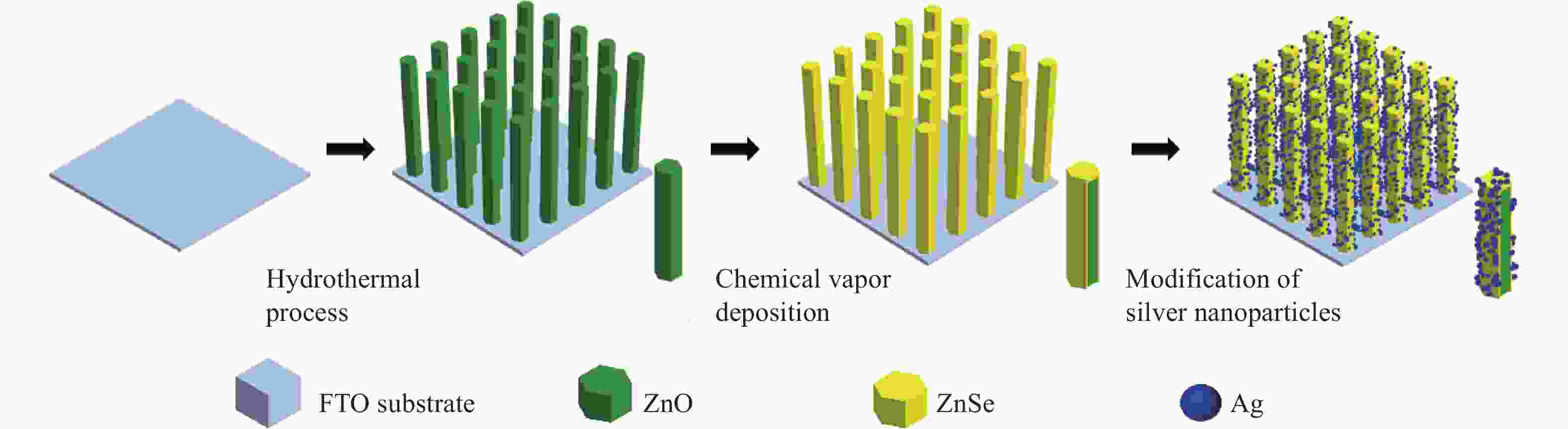
图 1 等离子体增强型ZnO/ZnSe异质结阵列光电探测器制备流程示意图
Figure 1. Schematic of preparation process of plasmon-enhanced ZnO/ZnSe heterojunction array photodetector
-
通过扫描电子显微镜(SEM)观察了样品的微观形貌,通过X射线衍射仪(XRD)和显微共焦拉曼光谱仪(Raman)分析了样品的化学组成和晶体成分,通过德国Zahner电化学工作站对样品的光电性能进行了测试。
-
文中采用德国Zahner电化学工作站三电极系统对该Ag纳米颗粒增强的ZnO/ZnSe异质结阵列进行光电性能测试。其中,该光电探测器作为工作电极,Ag/AgCl电极为参比电极,铂电极为对电极,电解液为0.5 mmol/L的Na2SO4溶液,照明光源为波长范围在430~720 nm的白光LED,采用了标准的斩光伏安法、光电瞬态测试系统和时间电流曲线对探测器的光电性能进行了测试分析。
-
合成ZnO纳米线阵列、ZnO/ZnSe异质结纳米线阵列和Ag纳米颗粒增强的ZnO/ZnSe异质结阵列的电镜照片如图2(a)~(c)所示。水热法所制备的ZnO纳米线成阵列均匀生长,表面呈六边形形状(SEM图见图2(a))。通过化学气相沉积,Se2−原位取代了ZnO纳米线中O2−,形成了较薄的ZnO/ZnSe异质结(TEM图见图2(b))。图2(c)是Ag纳米颗粒增强的ZnO/ZnSe异质结纳米线阵列的SEM图像。Ag纳米颗粒分布在纳米线阵列表面。
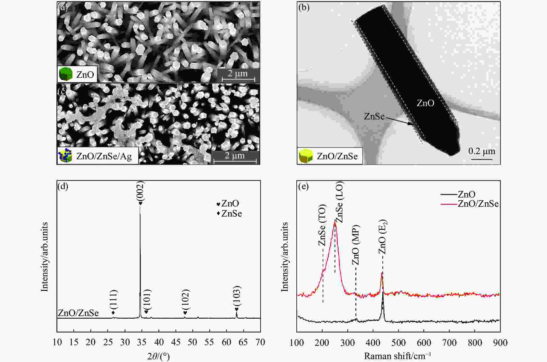
图 2 一维异质结纳米线阵列微观形貌图及物相表征图。(a) ZnO纳米线的SEM图像;(b) ZnO/ZnSe异质结的TEM图像;(c) Ag纳米颗粒增强的ZnO/ZnSe异质结纳米线阵列的SEM图像;(d) ZnO/ZnSe异质结的X射线衍射能谱图;(e) ZnO纳米线与ZnO/ZnSe异质结的拉曼光谱图
Figure 2. Microstructure and phase characterization of 1-dimensional (1D) heterojunction nanowire arrays. (a) SEM image of the ZnO nanowires; (b) TEM images of the ZnO/ZnSe heterojunctions; (c) SEM image of the ZnO/ZnSe core-shell heterojunction nanowire arrays enhanced by Ag nanoparticles; (d) X-ray diffraction spectrum of the ZnO/ZnSe heterojunctions; (e) Raman spectra of the ZnO nanowire and ZnO/ZnSe heterojunction
利用X射线衍射(XRD)和显微共焦拉曼光谱(Raman)对样品的物相组成进行了表征,如图2(d)、图2(e)所示。ZnO/ZnSe异质结的XRD(图2(d))可以明显的发现(002)、(101)、(102)和(103)的晶面衍射峰,对应ZnO的纤锌矿结构。峰强最大在(002)晶面处,表明ZnO纳米线在FTO表面沿c轴取向优先生长,结晶质量较好。27.1°处的小峰对应于ZnSe的(111)晶面,且只有一个微弱峰出现,表明在ZnO/ZnSe异质结材料中,ZnSe的含量低于ZnO[15−16]。
ZnO纳米线与ZnO/ZnSe异质结纳米线阵列的拉曼光谱如图2(e)所示。位于205、250 cm−1的峰分别对应立方闪锌矿ZnSe晶体结构的横向光学(TO)声子模和纵向光学(LO)声子模[15,17]。位于332 cm−1处的峰对应于ZnO多光子(MP)散射过程;位于440 cm−1处的峰属于ZnO非极性光学声子模的高频分支,该模是纤锌矿ZnO的特征模之一,较强的E2模表明ZnO纳米线沿c轴方向生长良好。因此,XRD和TEM结果一致证实了ZnO/ZnSe异质结纳米线阵列的形成。
-
器件的光响应度R被定义为其响应入射光信号的能力,根据光电探测器的I-V特性,计算公式如下[18]:
$$ R = (I_{{\rm{light}}}-I_{{\rm{dark}}}) / P_{{\rm{opt}}}A $$ 式中:Ilight为光电流;Idark为暗电流;Popt为入射光功率密度;A为有效照射面积,响应度R反映了光电流的光电转换能力。ZnO纳米线阵列光电探测器、ZnO/ZnSe异质结纳米线阵列光电探测器和Ag纳米颗粒增强的ZnO/ZnSe异质结纳米线阵列光电探测器在−0.8~0.6 V偏置电压下的斩光伏安(I-V)曲线图如图3(a)所示,在可见光照射下,Ag纳米颗粒增强的ZnO/ZnSe异质结纳米线阵列光电探测器的光响应度远大于ZnO/ZnSe异质结纳米线阵列光电探测器和ZnO纳米线阵列光电探测器,最高达2.8 mA/W。其机理如图3(b)所示,ZnO/ZnSe异质结纳米线阵列的内建电场促进了光生电子-空穴对的有效分离。径向结构异质结有效减小了载流子在被电极收集之前必须扩散的距离,从而抑制了复合并提高了收集效率,加强了异质结界面的电子输运特性。垂直排列的纳米线阵列具有优异的光吸收能力,在这种结构中,吸收边取决于异质结中较低的带隙材料,从而能实现更强的光吸收。此外,Ag纳米颗粒利用等离子体增强效应有效局域了入射光场,也极大地促进光电探测器的光吸收,从而增加其光电流密度。

图 3 (a) 一维异质结纳米线阵列光电探测器在-0.8~0.6 V偏置电压下的斩光I-V曲线图; (b) Ag纳米颗粒增强的ZnO/ZnSe异质结纳米线阵列光电探测器能带结构示意图
Figure 3. (a) The chopped I-V curve of 1D heterojunction nanowire array photodetector at −0.8 - 0.6 V bias voltage; (b) Schematic of energy band structure of ZnO/ZnSe heterojunction nanowire array photodetector enhanced by Ag nanoparticles
在0.8 V偏压及100 mW/cm2的可见光照射下,基于ZnO纳米线、ZnO/ZnSe核/壳异质结纳米线阵列和Ag纳米颗粒增强的ZnO/ZnSe异质结纳米线阵列制备的光电探测器的光电流如图4(a)所示。Ag纳米颗粒增强的ZnO/ZnSe异质结纳米线阵列光电探测器的响应度约是单纯ZnO纳米线阵列光电探测器的52倍,其响应度为1.71 mA/W。这表明异质结的形成与Ag纳米颗粒修饰的确能够促进光电探测器中光生电子-空穴对的分离,增强材料的光电响应强度。在0.4 V偏压下,Ag纳米颗粒增强的ZnO/ZnSe异质结纳米线阵列光电探测器在不同光强下的光电流如图4(b)所示。可见,随着光照强度的增加,Ag纳米颗粒增强的ZnO/ZnSe异质结纳米线阵列光电探测器的光电流显著增加。

图 4 (a) 在0.8 V偏压、100 mW/cm2的可见光照射下,光电探测器的光电流图;(b) Ag纳米颗粒增强的ZnO/ZnSe异质结纳米线阵列光电探测器在0.4 V偏压、不同光强时对应的光电流
Figure 4. (a) Photocurrent diagram of the photodetectors at 100 mW/cm2 visible light intensity(@0.8 V); (b) Photocurrent of ZnO/ZnSe heterojunction nanowire array photodetectors reinforced by Ag nanoparticles at different light intensities(@0.4 V)
图5是探测器的紫外-可见吸收光谱。从这些吸光度曲线可以看出,ZnO纳米线阵列光电探测器在200~360 nm波长范围内具有较强的紫外吸收特性,这与ZnO半导体3.37 eV的固有带隙宽度是一致的。与纯ZnO纳米线阵列光电探测器相比,ZnO/ZnSe异质结纳米线阵列光电探测器在400~600 nm范围内的吸收明显增强,表明异质结的形成拓宽了器件对光谱的响应范围;Ag纳米颗粒增强的ZnO/ZnSe异质结纳米线阵列光电探测器在400~800 nm波长范围内的吸光度提高了5倍左右,表明Ag纳米颗粒可以不仅可以拓宽探测器对光谱的响应范围,而且极大地增强了对光的吸收强度。
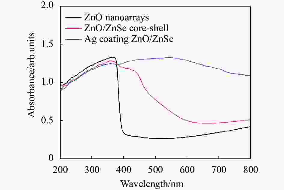
图 5 光电探测器的紫外-可见吸收光谱
Figure 5. UV–vis absorption spectra of the photodetectors
图6是探测器的奈奎斯特图,从图中可以看出,ZnO/ZnSe异质结纳米线阵列光电探测器与Ag纳米颗粒增强的ZnO/ZnSe异质结纳米线阵列光电探测器的阻抗非常接近,且都小于ZnO纳米线阵列光电探测器的阻抗值。阻抗值越小,说明光电探测器与电解质溶液在界面处的电子传输更快,光电流更高。结合图4(b),与单纯ZnO纳米线阵列光电探测器相比,形成异质结的一维ZnO/ZnSe异质结纳米线阵列光电探测器与等离子体增强型修饰增强的ZnO/ZnSe异质结纳米线阵列光电探测器的光电特性都有明显的提升。

图 6 探测器的奈奎斯特图
Figure 6. Nyquist plot of detectors
-
响应时间是指光电探测器将入射的光信号转化为电信号的弛豫时间,用来表征光电探测器追踪快速变化光信号的能力。响应速度是由电流的上升时间(τrise)和下降时间(τdelay)来测量,一般τrise(τdelay)定义为从最大电流的10%(90%)~90%(10%)的上升(下降)时间。
从图7(a)中可以看出,合成的ZnO纳米线阵列光电探测器、ZnO/ZnSe异质结纳米线阵列光电探测器、Ag纳米颗粒增强的ZnO/ZnSe异质结纳米线阵列光电探测器的响应速度均在毫秒级别,且响应速度依次加快。光电瞬态测试系统(图7(b))表明,一维ZnO纳米线经改性后的平均上升时间减少了约32%(τrise=1.812 ms),平均下降时间τdelay由原来的3.357 ms减小为1.803 ms,减少了54%左右,响应速度得到很大提升。

图 7 (a) 光电探测器的平均上升时间与下降时间柱状图;(b) 等离子体增强型ZnO/ZnSe异质结纳米线阵列光电探测器的瞬态光电流曲线图(@0.4 V)
Figure 7. (a) Bar graph of average rise time and delay time of photodetector; (b) Transient photocurrent curve of plasma-enhanced ZnO/ZnSe heterojunction nanowire array photodetector(@0.4 V)
-
为了表征器件的稳定性,实验测试了单纯的ZnO纳米线阵列光电探测器和Ag纳米颗粒增强的ZnO/ZnSe异质结纳米线阵列光电探测器随时间变化的电流曲线(图8)。单纯ZnO纳米线阵列光电探测器的光电流密度在10 h时迅速衰减至0.0142 µA/cm2,而Ag纳米颗粒增强的ZnO/ZnSe异质结纳米线阵列光电探测器的光电流密度保持在0.0835 µA/cm2。等离子体增强型ZnO/ZnSe异质结阵列光电探测器在10 h光照后仍保持48%的光电流密度,表明该光电探测器具有较好的使用寿命。相比于最初制备的器件,在空气中长时间放置后(15个月),其光电流密度维持在原来的52%左右,表明该光电探测器有较好的长期稳定性。

图 8 光电探测器的光电稳定性曲线(@0.2 V for 10 h)
Figure 8. Photoelectric stability curve for photodetector (@0.2 V for 10 h)
-
文中通过低温水热法、化学气相沉积法制备了了Ag纳米颗粒增强的ZnO/ZnSe异质结阵列光电探测器。相比单纯ZnO材料, Ag纳米颗粒增强的ZnO/ZnSe异质结纳米线阵列的响应度和响应速率得到了极大的提升,其响应度是ZnO纳米线阵列光电探测器的52倍,高达1.71 mA/W,其光电性能稳定,可广泛应用于新一代的光电子器件,如新型军用快速光电探测器件、快速光检测器等。
Plasmon-enhanced ZnO-based nanowire heterojunction array photodetector
-
摘要: 低维ZnO基光电探测器具有高响应性和高光子吸收能力。然而,ZnO较窄的吸收范围以及较低的光生载流子寿命限制了低维ZnO材料在光电子学中的潜在应用。该研究展示了一种零维(0D)金属纳米等离子体增强氧化锌纳米线(ZnO)-硒化锌(ZnSe)异质结阵列的新型光电探测器。与基于单纯ZnO纳米线阵列的探测器件比较表明,该探测器具有优异的光电响应性能。在可见光作用下,该器件的响应度和平均上升(下降)时间分别为1.7 mA/W和1.812 ms (1.803 ms),在10 h连续测试中表现出优异的稳定性,为开发高性能光电探测器提供了一种低成本、可规模化的方法,有望在可穿戴设备、光通信系统、环境传感器等多方面得到应用。Abstract:
Objective Low-dimensional ZnO-based photodetectors have high responsivity and high photon absorption ability. However, the limited absorption range and reduced carrier lifetime of ZnO constrain its potential applications in optoelectronics. This study presents a novel plasmon-enhanced photodetector with zinc oxide (ZnO) nanowires-zinc selenide (ZnSe) heterojunction arrays. Methods One-dimensional (1D) ZnO nanowires with ZnSe shell heterostructures were synthesized on FTO substrate using low-temperature hydrothermal and chemical vapor deposition methods. Subsequently, silver nanoparticles were uniformly deposited on the heterojunction through capillary self-assembly, resulting in a plasmon-enhanced heterojunction array photodetector (Fig.1). The built-in electric field within the heterostructure accelerates the effective separation of photogenerated electrons and holes, thereby promoting the charge carrier transport characteristics of the optoelectronic device. Leveraging the surface plasmon resonance effect, noble metal nanoparticles exhibit excellent localized field enhancement, effectively enhancing the material's light absorption. Material morphology, structure, and chemical composition were characterized through scanning electron microscopy (SEM), transmission electron microscopy (TEM), X-ray spectroscopy (XRD), and Raman spectroscopy analyses. The photovoltaic characteristics of the detector were systematically analyzed using standard techniques such as the chopped light voltammetry method, optoelectronic transient response measurement, and time-current curves. Results and Discussions Under visible light irradiation, the photoresponsivity of the Ag nanoparticle-enhanced ZnO/ZnSe heterojunction nanowire array photodetector far exceeds that of the ZnO/ZnSe heterojunction nanowire array photodetector and the ZnO nanowire array photodetector, reaching a maximum of 2.8 mA/W (Fig.3). At a bias voltage of 0.8 V and under visible light irradiation at 100 mW/cm2, the responsivity of the Ag nanoparticle-enhanced ZnO/ZnSe heterojunction nanowire array photodetector is approximately 52 times higher than that of the pure ZnO nanowire array photodetector, with a responsivity of 1.71 mA/W (Fig.4). This indicates that the formation of the heterostructure, coupled with Ag nanoparticle modification, indeed promotes the separation of photogenerated electron-hole pairs in the photodetector, enhancing the material's photodetection ability. Compared to the pure ZnO nanowire array photodetector, the ZnO/ZnSe heterojunction nanowire array photodetector exhibits significantly enhanced absorption in the range of 400 nm to 600 nm. Furthermore, the Ag nanoparticle-enhanced ZnO/ZnSe heterojunction nanowire array photodetector demonstrates an approximately 5-fold increase in absorbance within the wavelength range of 400 nm to 800 nm (Fig.5). This indicates that the formation of the heterostructure broadens the device's spectral response range. The presence of Ag nanoparticles not only extends the detector's spectral response range but also greatly enhances the intensity of light absorption. The optoelectronic transient testing system reveals that the average rise time of 1D ZnO nanowires is reduced by approximately 32% after modification (τrise=1.812 ms). The average delay time (τdelay) has decreased from the original 3.357 ms to 1.803 ms, representing a reduction of about 54%. This substantial improvement in response speed is illustrated (Fig.7). The current curve of the photodetector over time was tested, and the plasmon-enhanced ZnO/ZnSe heterojunction array photodetector maintained 48% of its photocurrent density after 10 hours of illumination, indicating favorable operational longevity. Compared to the initially fabricated device, the photodetector maintained approximately 52% of its photocurrent density after prolonged exposure to air (15 months), highlighting its robust long-term stability (Fig.8). Conclusions Compared with the detector based on pure ZnO nanowire array, the detector has excellent photoelectronic performance. Under visible light, the photodetector demonstrates responsivity of 1.7 mA/W and average rise/delay times of 1.812 ms (1.803 ms), exhibiting exceptional stability over 10 hours of continuous testing. This provides a cost-effective, scalable approach for developing high-performance photodetectors, with promising applications in wearable devices, optical communication systems, environmental sensors, etc. -
Key words:
- plasmonic enhancement /
- ZnO nanowire /
- nanowire heterojunction /
- photodetector
-
图 1 等离子体增强型ZnO/ZnSe异质结阵列光电探测器制备流程示意图
Figure 1. Schematic of preparation process of plasmon-enhanced ZnO/ZnSe heterojunction array photodetector
图 2 一维异质结纳米线阵列微观形貌图及物相表征图。(a) ZnO纳米线的SEM图像;(b) ZnO/ZnSe异质结的TEM图像;(c) Ag纳米颗粒增强的ZnO/ZnSe异质结纳米线阵列的SEM图像;(d) ZnO/ZnSe异质结的X射线衍射能谱图;(e) ZnO纳米线与ZnO/ZnSe异质结的拉曼光谱图
Figure 2. Microstructure and phase characterization of 1-dimensional (1D) heterojunction nanowire arrays. (a) SEM image of the ZnO nanowires; (b) TEM images of the ZnO/ZnSe heterojunctions; (c) SEM image of the ZnO/ZnSe core-shell heterojunction nanowire arrays enhanced by Ag nanoparticles; (d) X-ray diffraction spectrum of the ZnO/ZnSe heterojunctions; (e) Raman spectra of the ZnO nanowire and ZnO/ZnSe heterojunction
图 3 (a) 一维异质结纳米线阵列光电探测器在-0.8~0.6 V偏置电压下的斩光I-V曲线图; (b) Ag纳米颗粒增强的ZnO/ZnSe异质结纳米线阵列光电探测器能带结构示意图
Figure 3. (a) The chopped I-V curve of 1D heterojunction nanowire array photodetector at −0.8 - 0.6 V bias voltage; (b) Schematic of energy band structure of ZnO/ZnSe heterojunction nanowire array photodetector enhanced by Ag nanoparticles
图 4 (a) 在0.8 V偏压、100 mW/cm2的可见光照射下,光电探测器的光电流图;(b) Ag纳米颗粒增强的ZnO/ZnSe异质结纳米线阵列光电探测器在0.4 V偏压、不同光强时对应的光电流
Figure 4. (a) Photocurrent diagram of the photodetectors at 100 mW/cm2 visible light intensity(@0.8 V); (b) Photocurrent of ZnO/ZnSe heterojunction nanowire array photodetectors reinforced by Ag nanoparticles at different light intensities(@0.4 V)
图 7 (a) 光电探测器的平均上升时间与下降时间柱状图;(b) 等离子体增强型ZnO/ZnSe异质结纳米线阵列光电探测器的瞬态光电流曲线图(@0.4 V)
Figure 7. (a) Bar graph of average rise time and delay time of photodetector; (b) Transient photocurrent curve of plasma-enhanced ZnO/ZnSe heterojunction nanowire array photodetector(@0.4 V)
-
[1] Ren S, Gao S, Lu H, et al. A facile template-assisted synthesis of large-scale Bi2O3 nanotube arrays for self-powered UV photodetector [J]. Appl Surf Sci, 2022, 590: 153049. doi: 10.1016/j.apsusc.2022.153049 [2] Li C, Wang H, Wang F, et al. Ultrafast and broadband photodetectors based on a perovskite/organic bulk heterojunction for large-dynamic-range imaging [J]. Light Sci Appl, 2020, 9(1): 31. doi: 10.1038/s41377-020-0264-5 [3] Tiwari S, Veeralingam S, Badhulika S. ZnSe nanoflakes/ZnO quantum dots heterojunction-based bandgap engineered, flexible broadband photodetector on paper substrate [J]. Mater Res Bull, 2023, 166: 112374. doi: 10.1016/j.materresbull.2023.112374 [4] Chen Z, Wang J, Wu H, et al. A transparent electrode based on solution-processed ZnO for organic optoelectronic devices [J]. Nat Commun, 2022, 13(1): 4387. doi: 10.1038/s41467-022-32010-y [5] Kim D, Leem J Y. Synthesis of interface modified MoS2/ZnO heterostructure via simple hydrothermal method and their enhanced UV photodetection characteristics with ultrafast photoresponse speed [J]. Mater Res Bull, 2022, 150: 111767. doi: 10.1016/j.materresbull.2022.111767 [6] Shang S, Dong Y, Zhang W, et al. Fabrication and performance of UV photodetector of ZnO nanorods decorated with Al nanoparticles [J]. Nanomaterials, 2022, 12(21): 3768. doi: 10.3390/nano12213768 [7] Dutta D, Reddy K S, Badhulika S. Exfoliated Se nanoparticles decorated on MoS2/paper-based heterojunction as a flexible, self-powered and highly responsive photodetector [J]. Mater Sci Semicond Process, 2023, 164: 107610. doi: 10.1016/j.mssp.2023.107610 [8] Yin Z, Shan Y, Yu M, et al. Enhanced performance of UV photodetector based on ZnO nanorod arrays via TiO2 as electrons trap layer [J]. Mater Sci Semicond Process, 2022, 148: 106813. doi: 10.1016/j.mssp.2022.106813 [9] Patel M, Pataniya P M, Patel V, et al. Flexible photodetector based on Graphite/ZnO–WS2 nanohybrids on paper [J]. J Mater Sci: Mater Electron, 2022, 33(17) : 13771-13781. doi: 10.1007/s10854-022-08309-3 [10] Huang J, Li Q, Lu, X, et al. LSPR-enhanced pyro-phototronic effect for UV detection with an Ag–ZnO schottky junction device [J]. Adv Mater Interfaces, 2022, 9(23): 2200327. doi: 10.1002/admi.202200327 [11] Shi Z, Xu T, Wu D, et al. Semi-transparent all-oxide ultraviolet light-emitting diodes based on ZnO/NiO-core/shell nanowires [J]. Nanoscale,, 2016, 8(19): 9997-10003. [12] 刘苹, 徐威, 熊峰, 等 . 光生载流子FN隧穿的范德华垂直异质结光电探测特性 [J]. 红外与激光工程,2023 ,52 (6 ):20230217 . Liu Ping, Xu Wei, Xiong Feng, et al. Photodetection properties of van der Waals vertical heterostructures based on photogenerated carrier-dominated FN tunneling [J]. Infrared and Laser Engineering, 2023, 52(6): 20230217. (in Chinese)[13] Mandavkar R, Kulkarni R, Lin S, et al. Significantly improved photo carrier injection by the MoS2/ZnO/HNP hybrid UV photodetector architecture [J]. Appl Surf Sci, 2022, 574: 151739. doi: 10.1016/j.apsusc.2021.151739 [14] Wang X, Li G, Peng J, et al. The Au/ZnSe/ZnO heterojunction improves the electron transfer behavior to enhance the detection performance of ascorbic acid [J]. J Alloys Compd, 2021, 873: 159721. doi: 10.1016/j.jallcom.2021.159721 [15] Ghoul M, Braiek Z, Brayek A, et al. Synthesis of core/shell ZnO/ZnSe nanowires using novel low cost two-steps electrochemical deposition technique [J]. J Alloys Compd, 2015, 647: 660-664. doi: 10.1016/j.jallcom.2015.06.100 [16] Ghaemi-moghadam M, Hassanzadeh A, Rahmati A. Surface plasmon resonance and absorption features beyond the bandedge in ZnO nanorods array – Au heterostructures: Prediction and more accurate representation [J]. Plasmonics, 2022, 17(3): 1345-1354. doi: 10.1007/s11468-022-01632-9 [17] Kumar P, Singh J, Ramam K, et al. ZnSe/ZnSe: Ag nanoparticles: Synthesis, characterizations, optical and Raman studies [J]. J Nanosci Nanotechnol, 2013, 13(1): 377-383. doi: 10.1166/jnn.2013.6736 [18] . [J]. , 2023, 72(6): 068501. (in Chinese) DOI: 10.7498/aps.72.20222303 .2023 ,72 (6 ):068501 Liu Xiaoxuan, Sun Feiyang, Wu Ying, et al. Research progress of silicon nanowires array photodetectors [J]. Acta Physica Sinica, 2023, 72(6): 068501. (in Chinese) doi: 10.7498/aps.72.20222303 -

 点击查看大图

计量
- 文章访问数: 40
- HTML全文浏览量: 13
- PDF下载量: 12
- 被引次数: 0

