


 下载:
下载:


-
光谱分析技术是一种广泛应用的表征技术,涉及从工业生产到科学研究的诸多领域[1]。传统光谱仪通过衍射光栅或棱镜将光分解成不同波段的光谱信号,并通过光电探测器阵列记录每个信号的强度,从而获得整个被测波长范围的光谱信息。为了提高光谱的分辨率,可以通过增大光电探测器阵列规模或增大光栅和光电探测器线阵列之间的光路长度等方式,但存在体积大、复杂昂贵、适用性较差等缺点,限制了在现场快检、长时监测等小型化和便携式场景的应用[2]。近年来,微型光谱仪甚至芯片级的光谱仪引起了学术界和工业界的广泛关注[3-7]。例如,基于窄带法布里-珀罗共振滤波器阵列的微型光谱仪[8],基于胶体量子点阵列的微型光谱仪[9],基于Mie共振超表面滤波器阵列的微型光谱仪[10],基于组分调控的单纳米线光谱仪[11],基于随机宽带光谱响应的光子晶体微型光谱仪[12]等。与传统的台式光栅光谱仪相比,芯片上有限空间内的色散是片上光谱分析技术的关键因素。光谱分辨率受到不同光谱通道间串扰的限制。已有的研究报告显示,在使用窄带滤波器[8, 10, 13-15]或随机宽带滤波器[11, 16]的实验中,对于透射光谱获得大波长范围的低光谱串扰具有挑战。此外,基于亚波长结构的滤波器需要先进的制造技术,而且大多数周期性结构都会受到严重的尺寸影响[10, 17-18]。
近年来,图像编码技术成为一种很有前途的片上光谱分析技术,其中散斑图案通过散射/衍射[19-23]或干涉[24-26]产生对波长敏感的散斑图案。为了获得强色散效果,通常采用具有大量光学界面或光学模式的结构,从而在光传播过程中积累空间色散效应。一些常见的用于实现色散效应的结构包括无序孔阵列[19-20]、磨砂铝板[21]、磨砂玻璃[22]、安德森局部介质[23]、多模光纤[24-25]和多模波导[27]等。在这些情况下,可以将图像中每个点的光强度视为一个光谱通道,因此目标光谱的光谱成分被映射到光强分布。虽然图像传感器可以提供几乎无限的像素用于光谱编码,但通常需要物镜和大成像距离来确保高空间分辨率,以准确地从散斑图像中解析出光谱信息。这种厘米级的空间要求对于手机和平板电脑等移动终端而言是难以接受的。
文中介绍了一种基于CMOS图像传感器(CMOS Image Sensor,CIS)的超紧凑无透镜片上光谱分析系统,金纳米棒作为散射体直接集成在CIS表面。有限的空间色散造成散斑图像的相关性增加,为此我们提出了一种基于卷积神经网络(Convolutional Neural Network,CNN)的光谱重建方法,显著提高了对图像编码的解析能力,在可见光范围内获得对目标光谱峰值波长的准确测量。这种利用先进算法补偿硬件资源不足的集成式光谱检测方法有望在现场检测和分布式传感等方面对集成性和成本有较强要求的场景展现良好的应用潜力。
-
如图1(a)所示,整个器件由嵌入金纳米棒的PVP直接贴在CIS(SONY,IMX224 MQV,12 bit,1 280 pixel×960 pixel,像素大小为3.75 μm×3.75 μm)表面构成,整体厚度不超过2 mm,横向尺寸小于4×4 mm2。入射光中不同波长的光与散射结构发生不同的相互作用,具有空间中不同的传输行为,而不同波长光分量的组合就形成不同的光场分布,从而在CIS的探测器阵列上形成不同的散斑图像。这些散斑之间的差异,是后续解析出原始光谱信息的关键。相同波长间隔的散斑图像的相关性越低,说明色散结构的色散能力越强,有助于在片上限域空间内获得更好的光谱解析。
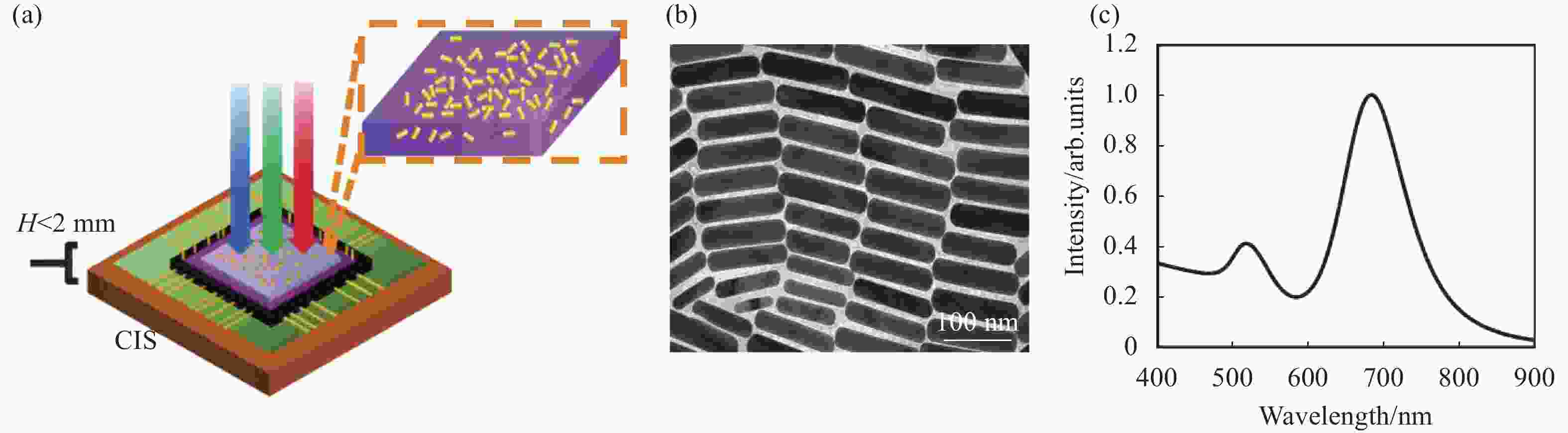
图 1 (a) 无透镜散斑编码光谱测试示意图,嵌入PVP膜层的金纳米棒直接覆盖在CIS表面;(b) 金纳米棒的透射电子显微镜图像;(c) 金纳米棒的消光谱
Figure 1. (a) Schematic of lens-free speckle image encoding experiment, where Au nanorods were embedded in a PVP film on glass, which is attached to the surface of a CIS; (b) TEM image of Au nanorods; (c) Extinction spectrum of Au nanorods
-
贵金属纳米颗粒支持表面等离子体共振,具有较大的散射截面,被广泛应用于光传感[28]、结构色[29]、光伏[30]等领域。空间随机分布的金属纳米颗粒具有丰富的热点分布,可以形成波长选择性的散斑图案,从而用于图像编码。相较于需要昂贵的自上而下图形化技术的规则纳米散射结构,化学合成的金属纳米结构具有低成本和大规模制备的优势。文中采用嵌入聚乙烯吡咯烷酮(Polyvinylpyrrolidone,PVP)中的金纳米棒作为散射结构进行散斑图像编码。
为了将金纳米棒嵌入PVP中,首先将平均分子量为58 000的PVP溶解在水中,并制成质量分数为500 mg/mL的胶体。其次,经离心分散的金纳米棒溶液在5 mM的CTAB溶液中浓缩约15倍。然后,将浓缩的Au纳米棒溶液加入到制备好的PVP胶体液中(VAu : VPVP= 2 : 5),并将混合溶液均匀旋涂在干净的石英片上。最后,样品在75 ℃下加热12 min,接着在30 ℃下烘干2 h。图1(b)显示了嵌入PVP的Au纳米棒透射电子显微镜图像,金纳米棒的排布并没有严格的规律性。沿着金纳米棒径向和轴向的偏振光分别会激发其两个偏振的表面等离子体共振,如图1(c)所示,683 nm波长处的主峰是轴向偏振,520 nm波长处的小峰是径向偏振。这些共振模式将在金纳米棒附近形成热点分布,提高散斑对比度。进一步考虑CIS的有效工作波长范围,后续图像编码实验均在600~700 nm波长范围内进行。
-
基于图像编码的光谱检测技术作为一种非直接的光谱信息测量方法,首先需要进行波长相关的图像编码。文中采用单色仪以1 nm变化步长依次输出600~700 nm单色光,经准直后照射器件,并记录散斑图像。从每张原始散斑图像中裁剪出一个1 220 pixel×900 pixel的部分,然后进一步将其分割成10×9个图像块,每块122 pixel×100 pixel像素点,将对应的波长信息作为这一批散斑数据的标签,以此作为神经网络的训练数据输入到神经网络中进行训练。
-
上述散斑图像包含了确定的波长信息,但图像和波长间的函数关系非常复杂,一般的解析方法和光谱重构算法都很难准确解析出原始光谱信息。基于CNN的深度学习方法通过大量的散斑数据训练,能够显著提高图像编码的解析能力[31]。CNN一般由多个阶段组成,每个阶段包含三个层:卷积层、激活层和池化层,每个阶段通过全连接的分类模块进行连接。这种层次结构的级联方式能够进行多层特征学习,并且在每一层中提取图像的深层特征。一般而言,增加网络的深度可以学习到更加具有区分性和独特性的信息。添加卷积和池化层可以提取数据中更高层次的特征的同时,还能够提供平移不变性的优势。通过使用较小的卷积和池化操作,可以减少网络中的参数数量,从而使网络进入深度学习。
每个卷积层对输入数据进行卷积计算,使用一组经过训练的滤波器来检测特定的特征。卷积层和激活层的权重和偏置在训练过程中进行计算。第n层中第j个特征图的活动计算如下:
$$F_j^n=g\left(\sum_i^{N_f}\left(W_{i, j}^n * {~F}_{{i}}^{{n}-1}+{b}_{{j}}^{{n}}\right)\right) $$ (1) 式中:Nf表示(n−1)层特征图的数量;$ {F}_{i}^{n-1} $∈Rm×n表示第(n−1)层的第i个特征图谱,它连接到第n层中的$ {F}_{i}^{n} $;$ {W}_{i,j}^{n} $∈Rk×k表示对于$ {F}_{i}^{n-1} $的大小为k的卷积核;$ {b}_{j}^{n} $表示偏差;g(...)表示非线性激活函数。在卷积层和激活层之后通常跟随一个池化层,其目的是提高模型的鲁棒性。最常用的池化算法是最大池化,在输入的特征图的局部窗口中找到最大值。通过使用大于1的步长进行下采样,可以有效减少参数数量,从而降低计算复杂度。最常见的池化滤波器大小是2×2,它能减少一半输出特征图的空间维度。CNN最后一个模块通常由几个全连接层组成,类似于传统的人工神经网络(ANN)[32]。全连接层的作用是将之前的卷积和池化层中提取的高级特征展平成一个固定维度的向量。这样做可以为最终的分类或回归任务提供准备。由第n个全连接层学习到的特征向量可以表示为:
$$ F^n=g\left(W^n * {~F}^{n-1}+{b}^{{n}}\right) $$ (2) 式中:Wn为连接第(n−1)层和第n层的权值矩阵;Fn−1为第(n−1)层中的特征向量;bn为第n层的偏置向量。输出层由一个softmax激活函数组成,用于计算每个类别的预测概率。CNN的监督训练使用一种随机梯度下降的形式,通过最小化真实标签和网络预测之间的差异来进行。如果输出层由softmax激活函数组成,则损失函数由交叉熵损失给出:
$$ {L}_{i}=-\log(p\left({y}_{i}|{f}_{i}\right)) $$ (3) 式中:Li为样本i的损失;fi为输入向量。数据集的全部损失是所有训练示例中Li的平均值。在训练阶段,每次迭代过程中,所有层中所有滤波器的系数都同时更新。
如图2所示,用Pytorch框架构建了一个五层深度学习CNN结构,黄色方体代表卷积层,橙色代表池化层,卷积层与池化层交替覆盖,经过一系列卷积池化后,再经过三层全连接层,最后到达输出层。122×100代表上述图像块大小,64、128、256、512代表卷积核个数(卷积核大小为3×3,池化层大小为2×2),紫色代表全连接,4 096代表全连接层的节点个数,最后的输出层265个节点,代表590~710 nm波长范围内的光谱强度值。在每一次迭代的过程中不断优化网络参数,使重构值与原始标签间的损失函数收敛,通常网络的迭代过程需要至少1 000次。此外,文中将这些图片和标签用进行随机打乱,使得网络迭代过程中每一批训练的数据能涵盖大部分波长标签,进而有力地增强了网络的泛化能力。在训练得到模型的网络参数后,就可以将未知光谱编码后的散斑输入网络,预测该散斑在各个波长下出现的概率,最后加权求和得到预测光谱。

图 2 光谱重构算法流程示意图
Figure 2. Schematic diagram of the flow of the spectral reconstruction algorithm
-
图3(a)~(c)分别显示了波长为600 nm、650 nm和700 nm的定标散斑图案。由于散射路径较短,散斑图案的对比度较低,不同波长的散斑图较难分辨,这也是通常使用图像编码进行光谱检测的工作都需要透镜或者长工作距离的原因[33-35]。图3(d)显示了650 nm波长对应散斑的强度瀑布图,这种分布包含了波长相关的特征信息。将每一个波长的散斑图中每个像素的输出数据排列成一个数列,并按波长顺序排成一个矩阵,就得到如图3(e)所示的响应矩阵。此响应矩阵对于一个固定的散射结构集成的CIS而言是固定的,将用于后续的光谱检测。为了体现不同色散结构的色散能力,定义谱相关度系数为:

图 3 (a)~(c) 600 nm,650 nm和700 nm波长入射光对应的散斑图;(d) 650 nm波长的散斑归一化强度瀑布图;(e) 响应矩阵;(f) 计算的谱相关度系数
Figure 3. (a)-(c) Speckle plots corresponding to incident light at 600 nm, 650 nm, and 700 nm; (d) Waterfall plot of speckle normalized intensity at 650 nm wavelength; (e) Response matrix; (f) Calculated spectral correlation coefficients
$$ C(X, Y)=\frac{\displaystyle\sum_1^z\left(X_i-\bar{X}\right)\left(Y_i-\bar{Y}\right)}{\sqrt{\displaystyle\sum_1^z\left(X_i-\bar{X}\right)^2\displaystyle \sum_1^z\left(Y_i-\bar{Y}\right)^2}} $$ (4) 式中:X和Y表示两个散斑图像,Xi和Yi表示这些图像中的单个像素,而$ {{\bar X}} $和$ {{\bar Y}} $表示它们的平均灰度值,z表示总像素数。C的归一化值反映了不同散斑图案之间的相关程度,C越大说明两个不同波长对应的散斑图案非常接近,即这个体系的色散能力较弱。对于一个固定的色散体系,波长间隔为0时C为1,波长间隔越大的两幅散斑图案的谱相关度系数会越小。一般用谱相关度系数下降到0.5的波长间隔来衡量色散能力。图3(f)为计算得到的图1架构的谱相关度系数,在100 nm波长间隔下C依然高达0.9,说明紧凑架构导致空间色散能力较弱。
-
集成式的光谱检测技术通常采用压缩感知算法进行光谱重构。不同于前述CNN算法,它是用如L1范数凸优化压缩感知算法基于响应矩阵和输出散斑求解输入光谱。这种算法在光谱通道的谱相关度系数较低时展示了较好的光谱解析效果[23-25]。图4(a)是使用前述CNN算法进行光谱解析的结果,重构光谱曲线与原始光谱高度吻合。而图4(b)~(d)是基于L1范数凸优化压缩感知算法对610 nm、630 nm、650 nm、670 nm和690 nm等五个单波长输入光产生散斑图案进行解码得到的重构光谱,由于散斑图像的谱相关度系数较高,重构结果非常差。这显示出深度学习算法可以有效地从大量的高相关度编码图像中提取光谱特征。图中黑线为商业光谱仪测试光谱,红线为基于文中技术的重构光谱,蓝线为基于压缩感知算法的重构光谱。

图 4 (a)基于CNN算法的光谱重构结果;(b)~(f)基于压缩感知算法的光谱重构结果
Figure 4. (a) Spectral reconstruction results based on CNN algorithm; (b)-(f) Spectral reconstruction results based on compressive sensing algorithms
除了单色仪输出的单色光谱,图5展示了对带通滤光片透射光谱和LED发光光谱的检测结果,其中滤光片对氙灯输出的宽带白光进行滤波和准直后作为测试光源。图5(a)中原始光谱峰值位置为632.07 nm,预测值为632.54 nm,误差为0.47 nm;图5(b)中原始光谱峰值位置为648.96 nm,预测值为648.51 nm,误差为0.45 nm。图5(c)中原始光谱峰值位置为671.27 nm,预测值为672.09 nm,误差为0.82 nm。图5(d)中原始光谱峰值位置为631.62 nm,预测值为630.7 nm,误差为0.92 nm。此外,所有情况下光谱谱形的吻合度也很高,体现了该技术较好的适用性。图中黑线为商业光谱仪测试光谱,红线为基于文中技术的重构光谱。

图 5 (a)~(c) 三个带通滤波片透射光谱的测试结果,632.8 nm(FWHM = 3 nm),650 nm(FWHM = 10 nm)和670 nm(FWHM = 10 nm);(d) LED发光光谱测试结果
Figure 5. (a)-(c) Test results of transmission spectra of three bandpass filters, 632.8 nm (FWHM = 3 nm), 650 nm (FWHM = 10 nm) and 670 nm (FWHM = 10 nm); (d) LED luminescence spectroscopy test results
-
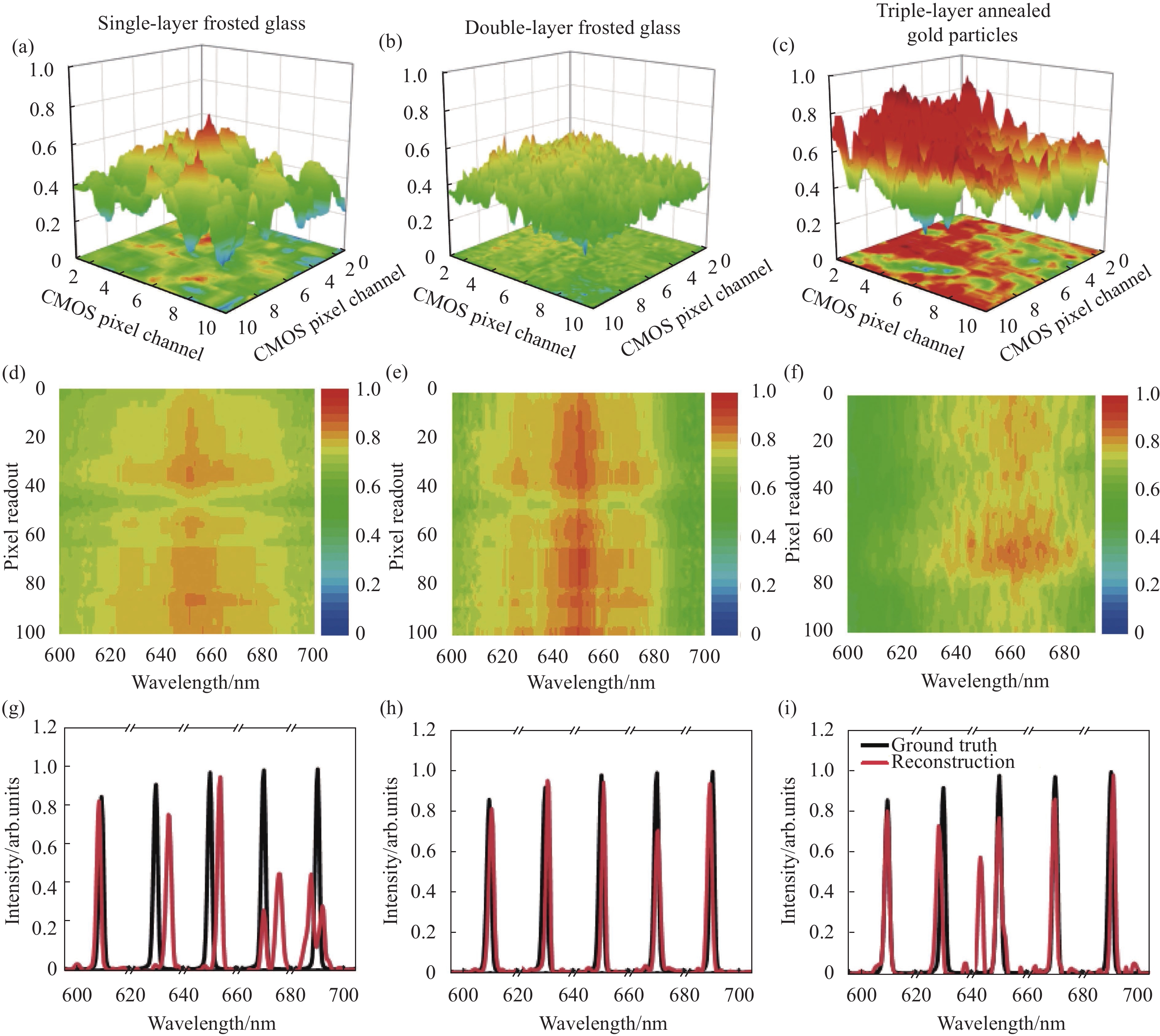
为了验证设计的CNN算法对不同散射结构的泛化能力,文中分别用单层毛玻璃、双层毛玻璃和三层退火金颗粒等替换金纳米棒进行类似实验。图6(a)~(c)分别为三种散射结构在650 nm波长对应的散斑强度瀑布图,图6(d)~(f)为不同结构相应的响应矩阵。可以看出,双层毛玻璃的散斑分布中峰谷位置变化比单层毛玻璃和三层退火金颗粒的更为复杂,其散斑图像包含更多的光谱特征信息。图6(g)~(i)所示的光谱重构结果也验证了这个结论。双层毛玻璃作为散射体的重构光谱(红色)与原始光谱(黑线)高度吻合,而其他两个散射结构的结果存在一些偏差。总的来说,三种散射结构都能较好的重构原始光谱,体现了文中提出的CNN算法的适用性。

图 6 (a)~(c) 单层毛玻璃,双层毛玻璃,三层退火金颗粒作为散射结构时,在650 nm波长处形成的散斑强度瀑布图,纵坐标为CIS读出数据对读数量程最大值的归一化;(d)~(f) 响应矩阵;(g)~(i) 黑线为商业光谱仪测试光谱,红线为基于文中技术的重构光谱
Figure 6. (a)-(c) Waterfall plot of speckle intensity at 650 nm wavelength when single-layer frosted glass, double-layer frosted glass and triple-layer annealed gold particles are used as scattering structures, and the ordinate is the normalization of the CIS readout data to the maximum value of the reading range; (d)-(f) Response matrix; (g)-(i) The black line is the test spectrum of the commercial spectrometer, and the red line is the reconstructed spectrum based on the proposed technology
-
文中提出了一种金纳米颗粒在CMOS图像传感器表面集成的片上光谱检测新技术架构。基于散斑成像,提出了无需透镜的光谱编码和解码技术,并利用CNN算法有效提高了限域空间中光谱解析的能力,实现了超紧凑的片上集成光谱检测功能,重构光谱与原始光谱吻合度高,适用性好。这种高集成、低成本的光谱检测技术有望在现场快检和分布式光谱采样的场景得到应用。
Integrated spectral detection based on lensless speckle image coding
-
摘要: 近年来,片上光谱检测技术由于其优异的集成特性在各种应用中引起了广泛的关注。得益于集成在各类便携式平台的低成本图像传感器,与波长相关的图像编码技术成为一种新兴的集成式光谱检测方法。为了准确地对图像中的光谱信息进行解码,通常需要物镜和较大的工作距离,这些都不可避免地增加了光学系统的复杂性和整个检测系统的尺寸。文中提出了一种基于卷积神经网络算法的新型散斑图像编码技术,通过将纳米散射结构直接集成到图像传感器表面进行散斑成像,实现了无需光学镜头的片上集成式光谱检测功能。这种高集成、低成本的光谱检测方法和器件利用先进算法克服了有限硬件资源造成的弱光谱检测能力,有望在现场快检和分布式传感网络等领域得到应用。Abstract:
Objective In recent years, on-chip spectroscopy has garnered considerable interests across multiple applications, primarily owing to its exceptional integration capabilities. Benefiting from mature image sensors with millions of pixels, wavelength-dependent image coding technology has emerged as a promising integrated spectroscopy method. However, achieving accurate decoding of spectral information in the images typically requires objective lenses and larger working distances, thereby increasing both the complexity of the optical system and the overall size of the inspection system. This limits its use in portable platforms such as mobiles. The aim of this work is to develop a lens-free image encoding method for on-chip spectroscopy and to address how to extract accurate spectral information from encoded images with high correlation. Methods A lens-free speckle image encoding method was developed for on-chip spectroscopy, where a PVP film embedded with Au nanorods was intimately integrated on an image sensor with a mm3 scale (Fig.1). The speckle of each signal wavelength was recorded to construct a responsive matrix for image encoding in advance. Although the image correlation is high in such a compact configuration (Fig.3), a convolutional neural network algorithm was applied to decode the image-spectrum relation by classifying the images with multilayer perceptron to extract high-level features (Fig.2). Once the calibration of image encoding is finished, the real-time spectral reconstruction takes only 1 s. Results and Discussions Spectral information was encoded in the speckle patterns generated by the Au nanorods. Conventional compressive sensing algorithm failed to reconstruct the original spectra due to the large image correlation in such a compact configuration (Fig.4). A convolution neutral network algorithm was developed to extract spectral features from low-contrast images and demonstrated accurate spectral reconstruction. For monochromatic light at 610 nm, 630 nm, 650 nm, 670 nm, and 690 nm, the deviation of the peak wavelength is consistently less than 1 nm in all cases (Fig.4(a)). Similar results were observed in the cases of single-layer frosted glass, double-layer frosted glass and triple-layer annealed gold particles, which shows the robustness of this method. The transmission spectra of three bandpass filters with varying filter ranges, as well as the emission spectra of a single LED were presented (Fig.5). And in every instance, the system predicts a wavelength peak deviation of less than 1 nm, with the spectral shape also demonstrating good agreement, indicating the applicability of the technology. Conclusions The work shows the possibility to develop an advanced image decoding algorithm based on convolution neutral network to compensate the limited hardware for on-chip spectroscopy based on image encoding. Such a ultracompact configuration together with decent spectroscopy performance enables potential applications in on-site inspection and distributed sensor network. -
Key words:
- microspectrometer /
- image encoding /
- scattering /
- deep learning
-
图 1 (a) 无透镜散斑编码光谱测试示意图,嵌入PVP膜层的金纳米棒直接覆盖在CIS表面;(b) 金纳米棒的透射电子显微镜图像;(c) 金纳米棒的消光谱
Figure 1. (a) Schematic of lens-free speckle image encoding experiment, where Au nanorods were embedded in a PVP film on glass, which is attached to the surface of a CIS; (b) TEM image of Au nanorods; (c) Extinction spectrum of Au nanorods
图 2 光谱重构算法流程示意图
Figure 2. Schematic diagram of the flow of the spectral reconstruction algorithm
图 3 (a)~(c) 600 nm,650 nm和700 nm波长入射光对应的散斑图;(d) 650 nm波长的散斑归一化强度瀑布图;(e) 响应矩阵;(f) 计算的谱相关度系数
Figure 3. (a)-(c) Speckle plots corresponding to incident light at 600 nm, 650 nm, and 700 nm; (d) Waterfall plot of speckle normalized intensity at 650 nm wavelength; (e) Response matrix; (f) Calculated spectral correlation coefficients
图 4 (a)基于CNN算法的光谱重构结果;(b)~(f)基于压缩感知算法的光谱重构结果
Figure 4. (a) Spectral reconstruction results based on CNN algorithm; (b)-(f) Spectral reconstruction results based on compressive sensing algorithms
图 5 (a)~(c) 三个带通滤波片透射光谱的测试结果,632.8 nm(FWHM = 3 nm),650 nm(FWHM = 10 nm)和670 nm(FWHM = 10 nm);(d) LED发光光谱测试结果
Figure 5. (a)-(c) Test results of transmission spectra of three bandpass filters, 632.8 nm (FWHM = 3 nm), 650 nm (FWHM = 10 nm) and 670 nm (FWHM = 10 nm); (d) LED luminescence spectroscopy test results
图 6 (a)~(c) 单层毛玻璃,双层毛玻璃,三层退火金颗粒作为散射结构时,在650 nm波长处形成的散斑强度瀑布图,纵坐标为CIS读出数据对读数量程最大值的归一化;(d)~(f) 响应矩阵;(g)~(i) 黑线为商业光谱仪测试光谱,红线为基于文中技术的重构光谱
Figure 6. (a)-(c) Waterfall plot of speckle intensity at 650 nm wavelength when single-layer frosted glass, double-layer frosted glass and triple-layer annealed gold particles are used as scattering structures, and the ordinate is the normalization of the CIS readout data to the maximum value of the reading range; (d)-(f) Response matrix; (g)-(i) The black line is the test spectrum of the commercial spectrometer, and the red line is the reconstructed spectrum based on the proposed technology
-
[1] Savage N. Spectrometers[J]. Nature Photonics , 2009, 3 (10): 601-602. [2] 郑麒麟, 文龙, 陈沁 . 基于散斑检测的微型计算光谱仪研究进展 [J]. 光电工程,2021 ,48 (3 ):200183 . doi: 10.12086/oee.2021.200183 Zheng Qilin, Wen Long, Chen Qin. Research progress of computational microspectrometer based on speckle inspection [J]. Opto-Electronic Engineering, 2021, 48(3): 200183. (in Chinese) doi: 10.12086/oee.2021.200183[3] Neece G A. Microspectrometers: an industry and instrumentation overview[C]//Imaging Spectrometry XIII, SPIE, 2008, 7086: 21-28. [4] Jayapala M, Lambrechts A, Tack N, et al. Monolithic integration of flexible spectral filters with CMOS image sensors at wafer level for low cost hyperspectral imaging[C]//International Image Sensor Workshop, 2013, 1. [5] Malinen J, Rissanen A, Saari H, et al. Advances in miniature spectrometer and sensor development[C]//Next-Generation Spectroscopic Technologies VII, SPIE, 2014, 9101: 83-97. [6] Saxe S, Sun L, Smith V, et al. Advances in miniaturized spectral sensors[C]//Next-Generation Spectroscopic Technologies XI, SPIE, 2018, 10657: 69-81. [7] Yang Z, Albrow-Owen T, Cai W, et al. Miniaturization of optical spectrometers [J]. Science, 2021, 371(6528): 0722. doi: 10.1126/science.abe0722 [8] Wang S W, Xia C, Chen X, et al. Concept of a high-resolution miniature spectrometer using an integrated filter array [J]. Optics Letters, 2007, 32(6): 632-634. doi: 10.1364/OL.32.000632 [9] Bao J, Bawendi M G. A colloidal quantum dot spectrometer [J]. Nature, 2015, 523(7558): 67-70. doi: 10.1038/nature14576 [10] Tittl A, Leitis A, Liu M, et al. Imaging-based molecular barcoding with pixelated dielectric metasurfaces [J]. Science, 2018, 360(6393): 1105-1109. doi: 10.1126/science.aas9768 [11] Yang Z, Albrow-Owen T, Cui H, et al. Single-nanowire spectrometers [J]. Science, 2019, 365(6457): 1017-1020. doi: 10.1126/science.aax8814 [12] Wang Z, Yi S, Chen A, et al. Single-shot on-chip spectral sensors based on photonic crystal slabs [J]. Nature Communications, 2019, 10(1): 1020. [13] Liang L, Hu X, Wen L, et al. Unity integration of grating slot waveguide and microfluid for terahertz sensing [J]. Laser & Photonics Reviews, 2018, 12(11): 1800078. [14] Wen L, Liang L, Yang X, et al. Multiband and ultrahigh figure-of-merit nanoplasmonic sensing with direct electrical readout in Au-Si nanojunctions [J]. ACS Nano, 2019, 13(6): 6963-6972. doi: 10.1021/acsnano.9b01914 [15] Wen L, Sun Z, Zheng Q, et al. On-chip ultrasensitive and rapid hydrogen sensing based on plasmon-induced hot electron–molecule interaction [J]. Light: Science & Applications, 2023, 12(1): 76. doi: 10.1038/s41377-023-01123-4 [16] Wu X, Gao D, Chen Q, et al. Multispectral imaging via nanostructured random broadband filtering [J]. Optics Express, 2020, 28(4): 4859-4875. doi: 10.1364/OE.381609 [17] John S. Strong localization of photons in certain disordered dielectric superlattices [J]. Physical Review Letters, 1987, 58(23): 2486. [18] Chen Q, Liang L, Zheng Q, et al. On-chip readout plasmonic mid-IR gas sensor [J]. Opto-Electronic Advances, 2020, 3(7): 190040. doi: 10.29026/oea.2020.190040 [19] Redding B, Liew S F, Sarma R, et al. Compact spectrometer based on a disordered photonic chip [J]. Nature Photonics, 2013, 7(9): 746-751. doi: 10.1038/nphoton.2013.190 [20] Yang T, Xu C, Ho H, et al. Miniature spectrometer based on diffraction in a dispersive hole array [J]. Optics Letters, 2015, 40(13): 3217-3220. doi: 10.1364/OL.40.003217 [21] Chakrabarti M, Jakobsen M L, Hanson S G. Speckle-based spectrometer [J]. Optics Letters, 2015, 40(14): 3264-3267. doi: 10.1364/OL.40.003264 [22] Yang T, Huang X L, Ho H P, et al. Compact spectrometer based on a frosted glass [J]. IEEE Photonics Technology Letters, 2016, 29(2): 217-220. doi: 10.1109/LPT.2016.2636340 [23] Kwak Y, Park S M, Ku Z, et al. A pearl spectrometer [J]. Nano Letters, 2020, 21(2): 921-930. doi: 10.1021/acs.nanolett.0c03618 [24] Redding B, Alam M, Seifert M, et al. High-resolution and broadband all-fiber spectrometers [J]. Optica, 2014, 1(3): 175-180. doi: 10.1364/OPTICA.1.000175 [25] Liew S F, Redding B, Choma M A, et al. Broadband multimode fiber spectrometer [J]. Optics Letters, 2016, 41(9): 2029-2032. doi: 10.1364/OL.41.002029 [26] Metzger N K, Spesyvtsev R, Bruce G D, et al. Harnessing speckle for a sub-femtometre resolved broadband wavemeter and laser stabilization [J]. Nature Communications, 2017, 8(1): 15610. doi: 10.1038/ncomms15610 [27] Redding B, Liew S F, Bromberg Y, et al. Evanescently coupled multimode spiral spectrometer [J]. Optica, 2016, 3(9): 956-962. doi: 10.1364/OPTICA.3.000956 [28] Chen Y, Ming H. Review of surface plasmon resonance and localized surface plasmon resonance sensor [J]. Photonic Sensors, 2012, 2: 37-49. doi: 10.1007/s13320-011-0051-2 [29] Chhatre A, Solasa P, Sakle S, et al. Color and surface plasmon effects in nanoparticle systems: Case of silver nanoparticles prepared by microemulsion route [J]. Colloids and Surfaces A: Physicochemical and Engineering Aspects, 2012, 404: 83-92. doi: 10.1016/j.colsurfa.2012.04.016 [30] Morawiec S, Mendes M J, Priolo F, et al. Plasmonic nanostructures for light trapping in thin-film solar cells [J]. Materials Science in Semiconductor Processing, 2019, 92: 10-18. doi: 10.1016/j.mssp.2018.04.035 [31] Kong W, Kuang D, Wen Y, et al. Solution classification with portable smartphone-based spectrometer system under variant shooting conditions by using convolutional neural network [J]. IEEE Sensors Journal, 2020, 20(15): 8789-8796. doi: 10.1109/JSEN.2020.2983733 [32] Berisha S, Lotfollahi M, Jahanipour J, et al. Deep learning for FTIR histology: leveraging spatial and spectral features with convolutional neural networks [J]. Analyst, 2019, 144(5): 1642-1653. doi: 10.1039/C8AN01495G [33] Meng Z, Li J, Yin C, et al. Multimode fiber spectrometer with scalable bandwidth using space-division multiplexing [J]. AIP Advances, 2019, 9(1): 015004. doi: 10.1063/1.5052276 [34] Li A, Fainman Y. On-chip spectrometers using stratified waveguide filters [J]. Nature Communications, 2021, 12(1): 2704. doi: 10.1038/s41467-021-23001-6 [35] Yang T, Peng J, Ho H, et al. Visible-infrared micro-spectrometer based on a preaggregated silver nanoparticle monolayer film and an infrared sensor card[C]//2017 International Conference on Optical Instruments and Technology: Optical Systems and Modern Optoelectronic Instruments, SPIE, 2018, 10616: 267-274. -

 点击查看大图

计量
- 文章访问数: 57
- HTML全文浏览量: 11
- PDF下载量: 22
- 被引次数: 0

