


-
短波红外探测器作为一种核心传感器,在感知与获取目标图像信息方面发挥着至关重要的作用。其显著特点包括穿透烟雾的能力、高空间识别度、全天候工作能力以及在恶劣天气条件下的适用性,这使得它在国家重大需求和国民经济发展的多个领域中具有广泛的应用价值[1]。在安防监控领域,它为低光照或无光照条件下的视频监控提供了强有力的技术支持[2],显著增强了安全保障能力。在环境监测方面,这些探测器通过精确测量大气中的特定成分,为环境保护和气候研究提供了宝贵的数据支持。此外,在医疗领域,短波红外探测器在疾病诊断中的应用,为医疗技术创新开辟了新的路径。因此,对短波红外探测器的深入研究具有重要的现实意义。
当前,短波红外探测器技术的发展呈现出多元化的技术路线。其中,基于铟镓砷的短波红外探测技术,经过数十年的持续研发,已在成像分辨率和制造技术方面取得了显著的突破[3]。凭借其高灵敏度、快速响应和低噪声等特性,铟镓砷探测器在军事侦察、航空航天等多个关键领域发挥了不可替代的作用[4]。然而,该技术在实际应用中仍面临制程与广泛应用的硅基CMOS半导体工艺不兼容以及高昂制造成本等挑战,这些因素限制了其大规模普及与应用。锗硅探测器是另一种备受关注的短波红外探测器,具备高响应速度和高量子效率等特点。得益于硅基锗薄膜外延技术的突破[5−6],锗硅探测器的性能得到了大幅度提升。然而,其截至波长位于通讯波长1550 nm附近,导致在1550 nm处的响应度易受温度波动的影响,同时暗电流偏大也成为了一个亟待解决的问题。最近几年,胶体量子点在短波红外探测领域的应用也逐渐崭露头角。尽管其仍面临稳定性和可靠性等方面的挑战,但由于胶体量子点具有可调谐的光学性质和高量子效率,在短波红外波段表现出了优异的响应性能[7−9]。
除了上述几种技术路线外,近年来,基于金属-硅形成的肖特基结中热电子发射原理进行红外探测的技术受到了研究者们的广泛关注[10−12]。在该类探测器中,当入射光子与金属相互作用时,能够有效激发金属中的热电子。这些热电子随后克服肖特基势垒,注入到硅材料中,进而诱导产生光电流。这种独特机制赋予了硅基肖特基结热电子探测器显著的优势:通过调控肖特基势垒的高度,可以灵活调整探测器的响应波段,有效拓展至短波红外区域,从而突破了传统硅基探测器因带隙限制而无法涉足的波段范围。此外,该技术的制造工艺与CMOS半导体工艺兼容,这使得金属-硅热电子探测器在成本控制方面具有很大的潜力,有望在民用领域实现大规模应用,为红外探测技术的发展带来重要突破。
尽管硅基肖特基结光电探测器具有多方面的优势,但其实际应用仍受限于较低的光电转换效率。鉴于此,文中系统地回顾肖特基光电探测器的光电转换机制,并围绕热电子的基本物理过程对国内外近期的研究成果进行了总结和分析。首先介绍了金属-硅肖特基结的形成及其基本特性,并探讨了热电子产生、传输和注入三个核心过程。接下来,在热电子的产生方面,回顾了研究人员通过光吸收增强和热损耗抑制等手段以提升热电子产生效率的相关工作。在热电子的传输方面,总结了当前提出的调控热电子初始位置、初始能量和动量分布、热电子自由程等方法,以提高热电子的传输效率。在热电子的注入方面,介绍了多肖特基结和界面调控等提高注入效率的策略。此外,鉴于暗电流对探测器性能的关键影响,还对当前的暗电流抑制方法进行了探讨。最后,对该领域未来的发展方向进行了展望。
-
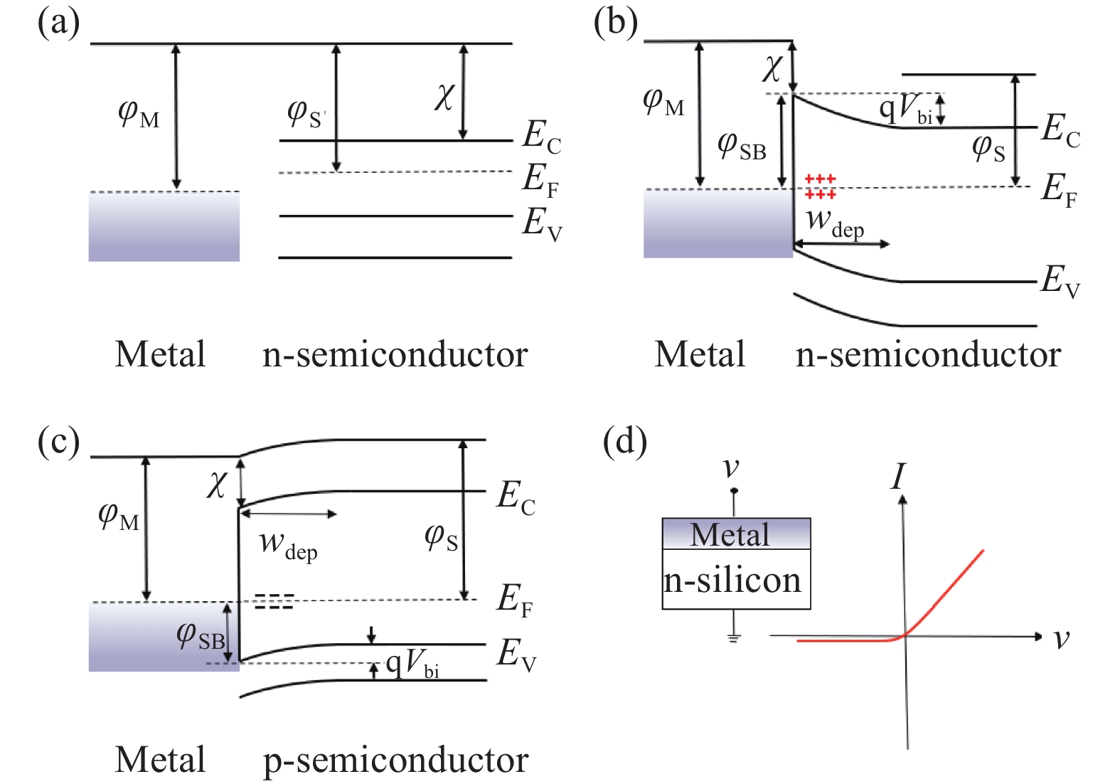
金属与硅形成肖特基结的过程是一个涉及电荷重新分布和电子能级调整的物理过程。如图1 (a)所示,对于N型硅,金属与硅接触后,N型硅由于费米能级一般高于金属的费米能级,导致N型硅的电子流向金属。在此过程中,半导体与金属接触的界面因电子转移而形成电场,电场的方向由半导体指向金属,又由于电场方向是电势降低的方向(也是电子的电势能升高的方向),因此N型硅的能带向上翘曲,形成如图1 (b)所示的能带结构。在理想情况下,金属与N型硅形成的肖特基结的势垒高度可由公式φ = Wmetal −χsi计算获得,其中φ为肖特基结势垒高度,Wmetal为金属的功函数,χsi为硅中电子的亲和势,代表硅导带底到真空的能量距离。如图1(c)所示,金属与P型硅形成肖特基结的过程与N型硅的情况类似,两者主要的不同点在于:N型硅肖特基结对应的热载流子一般为热电子,而P型硅肖特基结对应的热载流子通常是热空穴。

图 1 金属-硅肖特基结形成的原理示意图。 (a)金属和硅接触前的能带图; (b)金属和N型硅接触后的肖特基结能带图;(c)金属和P型硅接触后的肖特基结能带图;(d)肖特基结的典型电流-电压特性曲线
Figure 1. Schematic diagram of the formation principle of metal-silicon Schottky junction. (a) Energy band diagram before the contact between metal and silicon; (b) Energy band diagram of Schottky junction after the contact between metal and N-type silicon; (c) Energy band diagram of Schottky junction after the contact between metal and P-type silicon; (d) Typical current-voltage characteristic curve of Schottky junction
外加偏置电压的引入会打破肖特基结的热平衡状态,导致金属和硅之间的费米能级不再相等,从而改变了费米能级与肖特基结势垒的相对高度。具体而言,正向偏置时会使势垒相对高度降低,允许电子从金属流向硅中,形成正向电流;反向偏置则使势垒相对高度增加,阻止电子流动,电流几乎为零,展现了整流特性,如图1(d)所示。在实际情况中,肖特基势垒的高度由很多复杂因素决定,包括界面的性质、材料性质和制备条件等。在金属和硅之间形成肖特基势垒时,这些因素可以显著改变其高度。尤其是界面态可能会引发费米能级的钉扎效应,导致实际的肖特基势垒高度与理论预测值存在较大偏差。因此,在实际应用中,肖特基势垒的高度一般是通过实验测量来确定。
当红外光照射到金属-硅肖特基结探测器时,光子与金属内的电子发生相互作用,激发电子从低能量态跃迁至高能量态,形成热电子。这些热电子具备一定的初始动量分布,并在金属内部进行传输。其中,部分热电子会朝着肖特基结方向移动,并有一定几率越过肖特基势垒注入到硅材料中。成功注入硅中的热电子会继续向电极方向移动,最终形成可测量的电流,即光电流。如图2所示,光电流的形成过程涉及多个过程:首先是光子吸收导致热电子的产生,其次是热电子在金属内的传输,最后是热电子越过肖特基势垒注入硅材料。这些过程中均存在能量损耗,包括辐射损耗、热损耗、电子-电子、电子-声子相互作用引起的损耗等,导致大部分能量转化为热能而非电能。为了提高金属-硅肖特基结探测器的光电转换效率,须深入理解各阶段的能量损耗机制,并确立有效的策略来抑制这些损耗,增强光电流的产生。
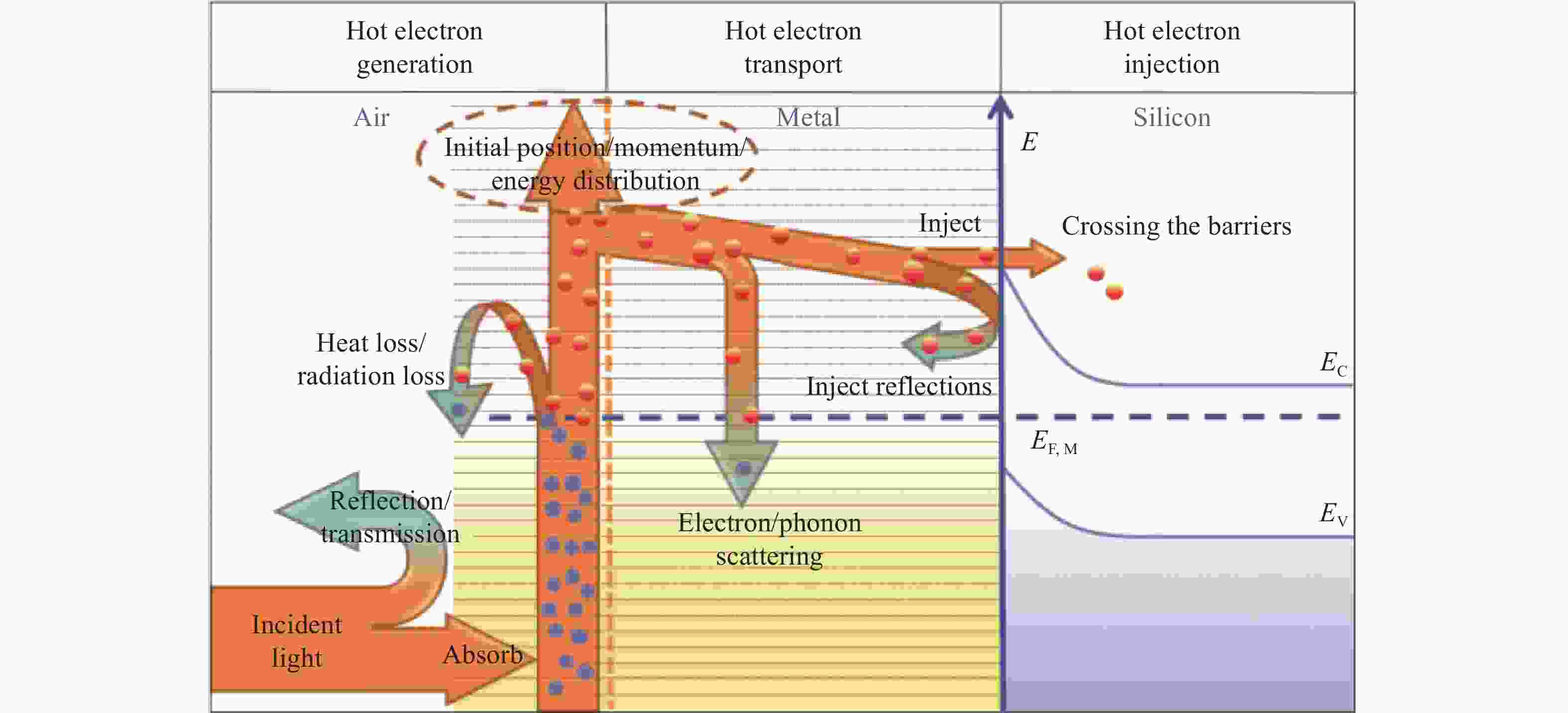
图 2 热电子产生、传输和注入三个阶段中能量的传递和损耗过程
Figure 2. The process of energy transfer and loss in the three stages of hot electron generation, transport, and injection
-
在金属中热电子的产生主要有两种方式[13−15]。第一种方式是入射光直接激发块体金属中的热电子。在这种情况下,光的吸收率对热电子的激发效率起着决定性作用,而块体金属会反射绝大部分的入射光,因而该种方式的热电子激发效率较低。第二种方式是光照射到金属纳米结构上激发表面等离激元共振[16−22]。这些等离激元在超快的时间尺度上(1~10 μs)发生弛豫。在这一过程中,等离激元可能通过多种方式衰减,包括通过朗道阻尼[23−24]退化成热电子-热空穴对,通过辐射衰减将能量以光子的形式发射,或者直接形成热损耗[25]。这些衰减机制的比例受到金属纳米结构的尺寸、材料种类以及热载流子的寿命等因素的影响[26−29]。因此,在热电子的产生过程中,光反射引起的损耗、等离激元的辐射损耗以及热损耗构成了主要的能量损失途径。为了提升热电子的产生效率,降低这些损耗机制至关重要。这需要对金属纳米结构[30−35]进行优化设计,以实现更高的光吸收率和更有效的等离激元转化过程。
激发的热电子的空间分布、初始能量和动量分布都对金属-硅肖特基探测器的光电转换效率具有重要的影响。首先,热电子在空间上的分布上并不均匀,这归因于金属不同区域光强度的差异,导致光强度较高的区域产生更多热电子。具体来说,热电子的空间分布可由下列公式给出:
$$ n\left(\stackrel{\rightharpoonup }{r},\omega \right)\propto \frac{1}{2\hslash }\mathrm{Im}\left(\varepsilon \right){\left|E\left(\stackrel{\rightharpoonup }{r},\omega \right)\right|}^{2} $$ 式中:n为热电子数目;E为入射光的电场;ω为入射光的频率;ε为金属的介电函数。由于入射光通常由多个频率组成,因此在计算热电子分布n时,需对频率进行积分。在探测器的设计中,优化热电子的空间分布,以确保其尽可能靠近肖特基结界面,可提升热电子注入硅中的概率。
其次,热电子的初始能量和动量分布也可能存在非均匀性[36−37]。在金属内部,原本位于费米能级(EF)以下的电子,在吸收入射光能量或由入射光激发的等离激元退化成热电子后,其能量将增加∆E,从而热电子的能量范围位于EF与EF+∆E之间。当电子的激发过程发生在同一能带内(即带内跃迁)时,受激发的电子态密度在EF以下通常呈现较为均匀的分布,使得激发后的热电子能量也在EF+∆E范围内均匀分布。然而,当电子发生带间跃迁时,情况则截然不同。此时,电子的态密度可能变得极为不均匀,导致热电子的能量分布也不均匀,如图3所示。

图 3 金属材料类型对热电子初始能量分布的影响
Figure 3. Effect of metal material type on initial energy distribution of hot electrons
以金属金为例,其d带电子主要位于费米能级下约2.6 eV的位置。当入射光子的能量超过此值时,会触发大量的d带电子的带间跃迁。这些跃迁后的电子大多位于费米能级附近,无法形成有效的热电子以越过肖特基势垒,从而对光电转换效率产生不利影响。另一方面,热电子的初始动量分布同样受到多种因素的影响,包括金属的晶体相对于硅界面的取向、入射光的电场方向以及带间跃迁等[36]。对于光电转换而言,理想的情形是电子的初始能量都高于肖特基势垒(而不是在EF+∆E范围均匀分布,或在势垒高度以下),电子的初始动量(速度)方向能够朝向肖特基界面,这样可增加其到达肖特基结界面的几率。因此,为了提升探测器的光电转换效率,须充分考虑热电子的初始能量分布以及动量分布特点。
-
热电子在产生后,必须传输至肖特基结的界面,才有可能成功注入硅中。在传输过程中,热电子会经历多种散射过程,主要包括电子-电子散射和电子-声子散射[38−43]。从动力学角度来看,热电子激发后在不同的时间尺度内展现出三种主要状态[36−44]。如图4 (a)所示,在小于10 μs的时间内,为金属吸收光后的热电子激发。而在大约10~100 μs的时间尺度内,热电子主要受到电子-电子散射过程的影响,导致其能量逐步降低,电子间的能量进行重新分配,形成一个准费米分布。当时间尺度超过100 μs时,电子-声子相互散射过程占据主导地位,使得电子与晶格之间发生能量交换,热电子逐渐冷却至平衡态,整个系统恢复到初始状态。因此,在热电子的传输过程中,电子-电子散射和电子-声子散射两个过程至关重要,它们直接决定了热电子是否能够成功到达金属-硅界面。这两种散射过程可以通过平均自由程来描述,其中电子-电子散射对应的平均自由程为lee,而电子-声子散射对应的平均自由程为lep。特别地,电子-电子散射的平均自由程lee并非一个常数,而是与热电子的能量高低密切相关。具体而言,能量较高的热电子更易于与其他电子发生碰撞,因此其自由程相对较短,而能量较低的热电子则拥有较长的自由程。另一方面,电子-声子散射的平均自由程lep主要受到声子数量的影响,与电子能量的关系并不显著[45−47]。由于声子的数量与温度有关,因此在特定温度下,可以认为lep是一个相对稳定的值。图4 (b)展示了金的平均自由程lee和lep,可以看出,在热电子能量小于2 eV的区间内,两种自由程均达到20 nm以上。

图 4 (a)热电子受到的散射过程及时间尺度; (b)热电子受电子和声子散射的平均自由程与热电子能量的关系
Figure 4. (a) The scattering process and time scale of hot electrons; (b) the relationship between the mean free path of hot electrons scattered by electrons and phonons and the energy of hot electron
受到电子-电子散射、电子-声子散射后,热电子从初始位置传输到肖特基界面的概率与激发点-界面的距离呈指数衰减关系,可由下面的公式给出[48]:
$$ P\left(\stackrel{\rightharpoonup }{r},E\right)=\frac{1}{2\pi }{\displaystyle \underset{\theta 1}{\overset{\theta 2}{\int }}\mathrm{exp}\left(-\frac{d\left(\stackrel{\rightharpoonup }{r}\right)}{l\left(E\right)\left|\mathrm{cos}\theta \right|}\right)}{\mathrm{d}}\theta $$ (1) 式中:$ P\left(\stackrel{\rightharpoonup }{r},E\right) $为r处激发的能量为E的热电子达到金-硅界面的概率;$ d\left(\stackrel{\rightharpoonup }{r}\right) $为r处热电子到金-硅界面的距离;$ \theta $为热电子的动量的方向;l(E)为热电子的自由程,由lee和lep根据马西森(Matthiessen)规则可以计算获得,即1/l(E)=1/lee + 1/lep。
因此,为提升热电子成功到达肖特基结界面的概率,可以从两个方面入手。首先是增加热电子的自由程。在金属材料内部缺陷较少的前提下,热电子的自由程主要由材料本身的类型所决定,因而可以采用具有较长自由程的材料。其次是缩短热电子初始位置与肖特基界面之间的距离。可通过调节入射光的电场分布使热电子的产生位置尽量靠近肖特基结界面,或者采用超薄金属材料将热电子限制在肖特基界面附近。
-
热电子到达金属-硅肖特基界面时并不一定都能够注入到硅中,其能量还必须满足一定的条件。具体而言,根据福勒(Fowler)模型,热电子垂直于肖特基界面的动能分量要高于势垒高度才能注入到硅中[49]。可认为热电子高于费米能级EF的能量部分为动能,在这种情况下,设热电子高于费米能级的能量为Ed,则有[49]:
$$ {E_{\rm{d}}} = \frac{{{{\left( {\hbar {k_{\rm{d}}}} \right)}^2}}}{{2m}} $$ (2) 式中:$\hbar {k_{\rm{d}}}$为热电子的动量大小,${k}_{{\rm{d}}}=\stackrel{\rightharpoonup }{\left|{k}_{{\rm{d}}}\right|}$为动量对应的波矢的模。根据上式,垂直于金-硅界面的能量部分可以表示为[49]:
$$ {E_{{\rm{d}} \bot }} = \frac{{{{\left( {\hbar {k_{{\rm{d}} \bot }}} \right)}^2}}}{{2m}} $$ (3) 式中:${k_{{\rm{d}} \bot }}$表示垂直于金-硅界面的动量。因此,只有这部分能量大于肖特基势垒高度的热电子才有可能注入到硅中,即满足如下的条件[37]:
$$ \hbar {k_{{\rm{d}} \bot }} > \sqrt {2m\varphi } $$ (4) 上式表示的注入条件对应的图像如图5所示,即在动量空间中,只有动量分布在红色锥形区内的那些热电子才可能注入。这个锥形区对应的临界角度为Ω,满足关系${k_{\rm{d}}}\cos \varOmega = \sqrt {2 m\varphi /{\hbar ^2}}$。因此,电子注入的概率就是对这个阴影区的立体角进行积分,再除以总的立体角,即有[49]:
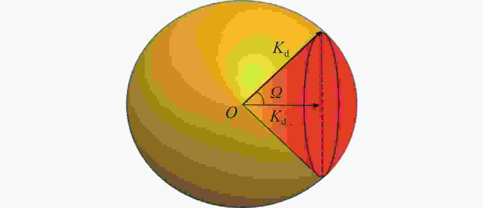
图 5 能够注入到硅中的热电子动量的锥形分布
Figure 5. The conical distribution of the momentum of hot electrons that can be injected into silicon
$$ P\left( {{E_{\rm{d}}}} \right) = \frac{{{\varOmega _{\rm{s}}}}}{{4\pi }} = \frac{1}{{4\pi }}\int\limits_0^{2\pi } {\int\limits_0^\varOmega {\sin \theta {\rm{d}}} } \theta {\rm{d}}\varphi = \frac{1}{2}\left( {1 - \cos \varOmega } \right) $$ (5) 又由于${k_{\rm{d}}}\cos \varOmega = \sqrt {2 m\varphi /{\hbar ^2}}$,可化简为$\cos \varOmega = \sqrt {\varphi /({\hbar ^2}{k_{\rm{d}}}/2 m)} = \sqrt {\varphi /{E_{\rm{d}}}}$。因此,上式可进一步简化为[49]:
$$ P\left( {{E_{\rm{d}}}} \right) = \frac{1}{2}\left( {1 - \sqrt {\frac{\varphi }{{{E_{\rm{d}}}}}} } \right) $$ (6) 从公式(6)可以看出,热电子的注入概率与其本身的能量Ed密切相关,Ed越大,注入效率越高。当Ed远远大于势垒高度φ时,注入概率趋近于0.5。这意味着高能量的热电子,只要其动量方向指向金属-硅界面,就有机会实现注入;但能量稍低的热电子要在动量方向在立体角Ω之内才能注入,如图5所示。未能成功注入的热电子会在界面处被反射回金属内部,其能量因各种散射过程而逐渐降低,这大大降低了它们再次注入到硅中的可能性。为了提高热电子的注入几率,可以采取多种策略。一种策略是采用双肖特基结、体肖特基结、粗糙表面等,这些结构通过增加金属与硅之间的接触面,扩大了可注入的角度范围,进而提高了注入效率。另一种策略是降低肖特基结势垒高度,但同时也会提高暗电流,进而影响探测器的信噪比。因此需综合考虑探测器的信噪比来决定是否采用该方法。
-
本节主要概述光学吸收增强的各种方法,以及抑制辐射损耗和热损耗的有效手段。这些方法和手段都能够提升热电子的产生效率。
-
光吸收是探测器实现光电转换最基本且最关键的步骤,通过增强光吸收可促进探测器中热电子的生成,从而提高光电转换效率。为了增强光吸收性能,研究者们提出了一系列创新方法,包含利用周期性或随机排列的纳米结构以增加光场的局部化[35, 50],采用平面叠层结构的谐振腔或抗反射膜来增加光吸收。下面分别对这些方法中的代表性工作进行介绍。
采用周期性纳米结构来增强探测器的光学吸收是目前应用最为广泛的方法。2011年,Knight等报告了一种金等离激元天线周期阵列增强的硅基热电子探测器,金等离激元天线一方面可以在共振波长处增强光吸收[51],同时在其内部还能产生热电子注入到硅中。研究发现,天线的长度影响共振吸收的波长,进而影响光电流的大小。当天线从110 nm变化到158 nm时,对应的谐振波长约从1250 nm增加到1500 nm,在谐振波长处探测器响应率达到最大值,这说明通过提高金天线的吸收率,可以提升热电子探测器的光电转换效率。
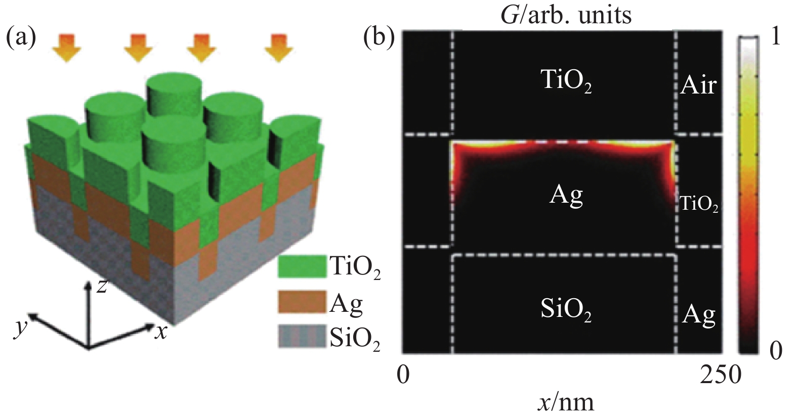
2014年,Lin等提出了深沟槽/薄金属等离激元天线结构增强的金-硅热电子探测器[52],能够在1250~1650 nm范围内实现宽光谱高效吸收,峰值吸收率达到88%。作者通过比较纳米棒、纳米片和纳米孔阵列天线,发现结构天线对应的器件的光吸收率、吸收带宽和响应度均优于其它天线结构。
同年,Li等人提出了一种通过利用超材料完美吸收结构来增强热电子探测器的光响应性能的方法,如图6所示。他们对偏振敏感的一维结构和偏振不敏感的二维结构进行了深入的研究[53]。结果发现,在1200~1500 nm波段内,两种结构的吸收率均能达到约50%,而峰值吸收率则超过90%。基于这种结构所制作的热电子探测器,其峰值响应度也高达3.37 mA/W。此外,二维结构的吸收率对入射光的角度并不敏感,即便在入射光角度为60°的情况下,仍能维持90%的吸收率。
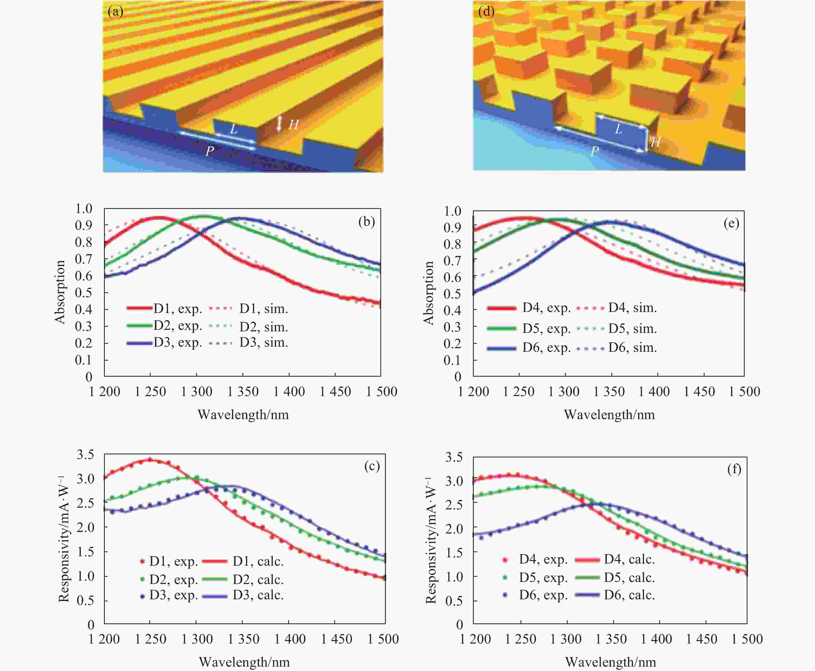
图 6 (a)、(b)基于一维和二维超材料完美吸收器的光电探测器示意图;(b)、(c)和(e)、(f)分别为(a)和(b)图探测器对应的吸收和响应曲线
Figure 6. (a), (b) Schematic diagram of a photodetector based on a one - and two-dimensional metamaterial perfect absorber; (b), (c) and (e), (f) are the absorption and response curves corresponding to the detectors in figure (a) and (b), respectively
相较于周期结构,平面叠层结构和随机纳米结构在制备工艺上更为简便。针对这些结构对光吸收的增强效果,研究者们也开展了深入的探索和研究。例如,2017年,Zhang等报道了利用分布式布拉格反射器,在金属/半导体/金属结构中集成热电子收集层,制作了基于Tamm等离激元的热电子探测器[54],如图7所示。通过强烈的Tamm等离激元共振,使得87%以上的入射光可以被金属层吸收。实验证明,纯平面和薄金属设计有利于实现高的光响应度,该类探测器的无偏光响应达到13.7 nA/mW,是同样工艺条件下常规的光栅耦合型器件(6.5 nA/mW)的2倍以上。
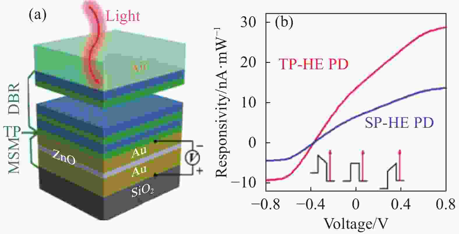
图 7 (a) Tamm等离激元增强型热电子探测器结构示意图; (b)其与光栅耦合增强型热电子探测器的响应度对比图
Figure 7. (a) Schematic diagram of the Tamm plasmon enhanced thermal electron detector; (b) Comparison diagram of its responsiveness with the grating coupled enhanced thermionic detector
2018年,Wen等报道了一种随机的光吸收增强结构的热电子探测器,如图8所示。首先,通过结合金退火和硅刻蚀的方法在硅表面制作随机的孔结构[55];随后,在这些孔结构上共形覆盖了一层薄金膜。这种随机结构能够在1~2 μm的宽波段范围实现接近90%的高效吸收,进而使得探测器的响应度达到了1.5~13 mA/W。2021年,Zhou等通过利用银离子辅助刻蚀硅的方法制备出无序金/硅纳米孔吸光结构[35],实现了多模局域等离子体共振,该探测器的吸收率达到82%,响应度可达0.34 mA/W。2023年,Zhang等设计了无序金/硅纳米针结构的热电子探测器[50],该结构在1200~2400 nm波段范围内平均吸收率高达97.3%,无偏压响应达到了2.56 mA/W。

图 8 (a)随机结构增强热电子探测器示意图;(b)不同退火温度下制备的Au/SiNH结构的吸收光谱;(c)不同Au涂层厚度的Au/SiNH器件的响应度;(d)不同照明模式下的响应度;(e)不同温度退火制备的Au/SiNH的扫描电镜(SEM)图像
Figure 8. (a) Schematic diagram of a random structure enhanced thermionic detector; (b) Absorption spectra of Au/SiNH structures prepared at different annealing temperatures; (c) The responsiveness of Au/SiNH devices with different Au coating thicknesses; (d) Responsiveness under different lighting modes; (e) Scanning electron microscopy (SEM) images of Au/SiNH prepared by annealing at different temperatures
-
对于入射光先激发金属等离激元,随后等离激元退化为热电子的产生机制。可以通过调控金属结构的尺度来优化降低热损耗的比例。这一方法有助于提高热电子的产生效率。
2013年,Govorov等人的一项研究揭示了金属纳米晶体尺寸对其热电子产生效率的重要影响[56]。具体而言,较大的金属纳米颗粒激发出的热电子能量相对较低,而直径小于20 nm的颗粒则能激发出能量更高的热电子。这一现象归因于纳米尺寸效应的存在,它打破了声子辅助热电子激发过程中所需满足的动量守恒条件。此外,研究还发现,当光场的偏振方向与纳米颗粒尺寸最小的方向一致时,更有利于热电子的产生。2014年,Manjavacas等人以球形势阱中的自由电子气模型为基础,深入研究了金属纳米球中的热电子产生过程。他们发现,颗粒尺寸和热电子寿命是决定热电子产生效率和能量分布的关键因素[57]。在颗粒尺寸较大且热电子寿命较短的情况下,热电子的产生效率会显著提升,但相应地,其能量水平较低。反之,当颗粒尺寸较小或热电子寿命较长时,热电子的能量会相对较高,但产生效率则会有所降低。
2016年,Brown等人采用第一性原理对等离激元的非辐射弛豫过程进行了深入分析。他们发现,在入射光子能量较低,不足以触发带间跃迁时,热损耗、几何和声子辅助的热电子激发过程相互竞争。然而,一旦带间跃迁被激发,直接的电子-空穴激发方式将占据主导[38]。值得注意的是,这些过程之间的比例可以通过调控纳米颗粒的尺寸和结构来优化,如图9所示。特别是当纳米颗粒的尺寸小于20 nm时,热损耗显著降低,而几何和声子辅助的热电子激发则成为主导因素。这一发现为等离激元材料的设计和优化提供了重要的理论依据。
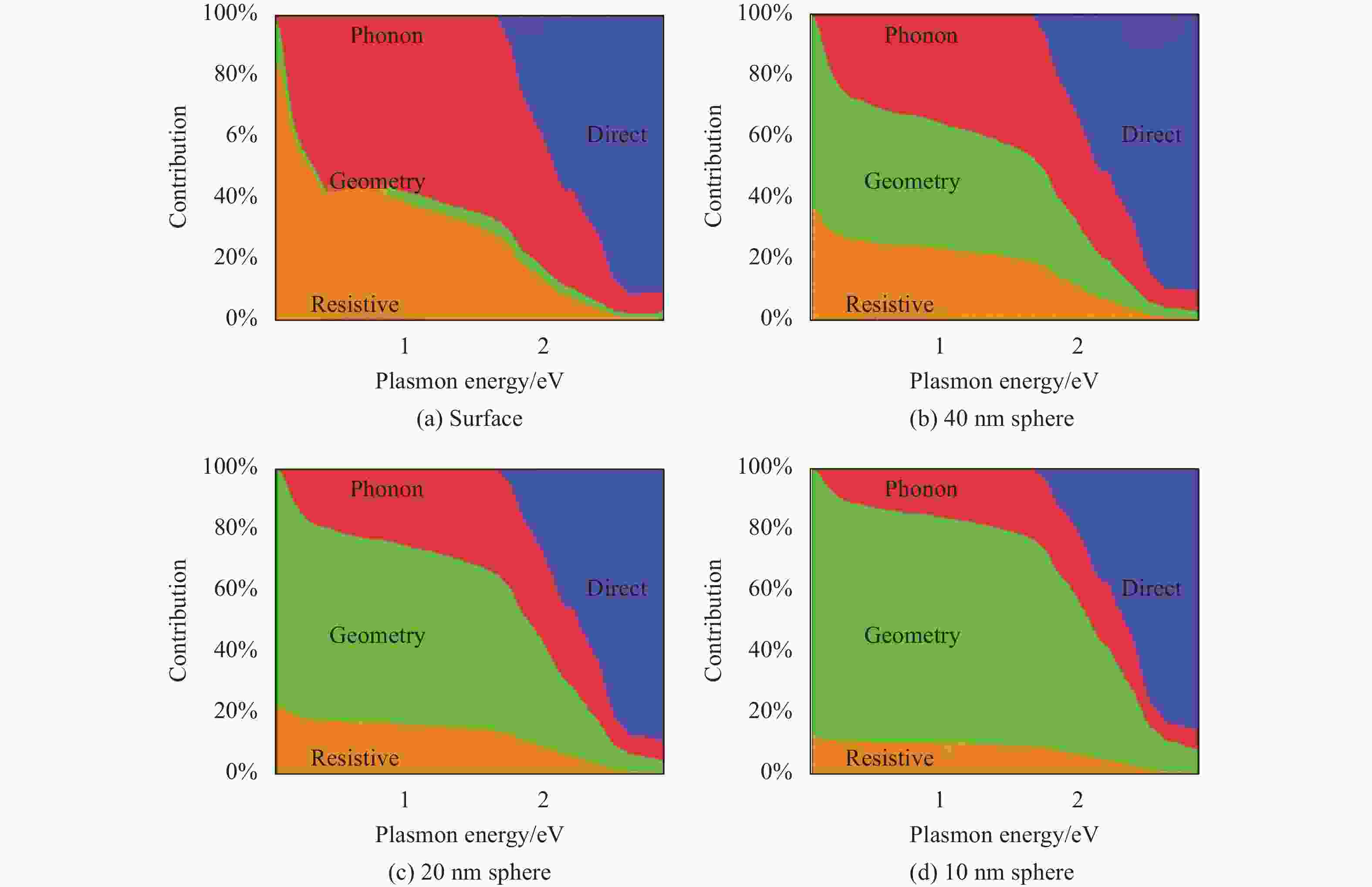
图 9 (a)半无限表面、 (b) 40 nm、(c) 20 nm和(d) 10 nm直径球体中的热损耗、几何辅助、声子辅助和直接跃迁占吸收总能量的百分比随频率变化的关系
Figure 9. The frequency variation of the percentage of heat loss, geometrical assist, phonon assist and direct transition to the total absorbed energy in (a) semi-infinite surface, (b) 40 nm, (c) 20 nm and (d) 10 nm diameter spheres
-
热电子产生时的初始位置、初始能量和动量、热电子的自由程对热电子传输到肖特基界面的概率都有很大的影响。本节将围绕这三方面对现有研究工作进行分析和总结。
-
从公式(1)可知,热电子从产生到传输到肖特基界面处的几率随传输距离呈指数衰减。因此,如果热电子在产生时就紧邻肖特基界面,将会显著提高其成功传输至该界面的几率,这对于优化热电子探测器的性能至关重要。
通过精心地设计表面等离激元的共振模式,可以使光场集中在肖特基结的界面。例如,2013年,Sobhani等设计了一种金属光栅结构,可在其上下表面激发表面等离激元,进而引发强烈的窄带共振吸收现象[16]。此过程中,大部分热电子在离肖特基界面近的金属层的底部产生,使得探测器响应度能提高到 0.6 mA /W,相对于纳米天线型探测器高 20 倍。2015年,南开大学Jia等将石墨烯插入金属纳米颗粒和氧化钛之间,可诱导等离激元的光场向金属纳米颗粒/氧化钛形成的肖特基结界面集中,从而增强了光电转换效率[58]。
2018年,苏州大学李孝峰团队提出了一种银纳米棒阵列结构,如图10 (a)所示。该结构激发等离激元共振时,会在银的顶部和侧壁形成两个高强度电场分布点,进而促进了热电子在肖特基结的界面生成,见图10 (b)。与传统的平面结构相比,这种金属纳米棒阵列结构将量子效率提高了近30倍[48]。同年,该团队通过在DBR(分布式布拉格反射结构)/金平面结构中激发Tamm等离激元,使光场局域在硅与金形成的肖特基界面附近,进而显著提升了热电子的传输效率[59]。
图 10 (a)银纳米棒阵列探测器结构图;(b)该探测器中热电子产生的初始位置
Figure 10. (a) Structure diagram of silver nanorod array detector; (b) The initial position of hot electron generation in the detector
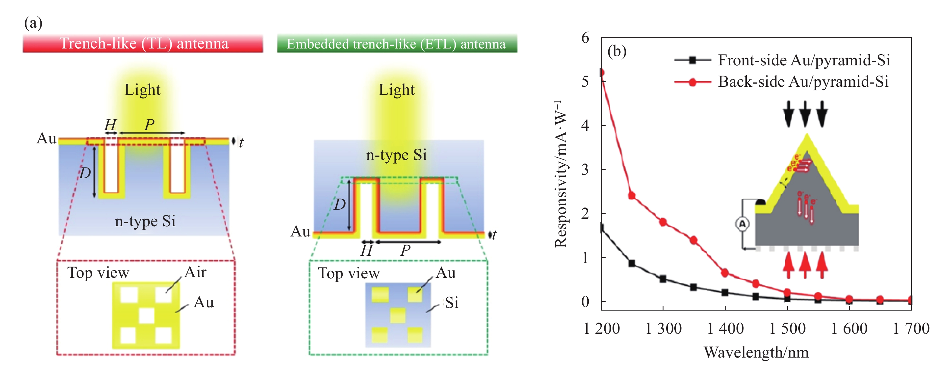
此外,当入射光从硅表面直接照射至肖特基界面(即背照式)时,能够有效地将热电子的产生位置集中在肖特基界面处,从而提升热电子的传输效率。例如,2018年,Duran等人对正照式和背照式测量方式下的Ni/Si肖特基热电子探测器的量子效率进行了对比研究,结果表明背照式下可使量子效率提升约50%[60]。进一步地,2019年Lin等人提出了基于沟槽式天线结构的热电子探测器[61]。如图11 (a)所示,通过正照和背照两种测试方式的对比实验,发现两种方式均能有效激发等离激元并促使热电子聚集在肖特基界面,但背照式下的光响应度更为显著。
2020年,Zhai等人设计了Au/Si微锥体结构的热电子探测器[22]。研究发现,在1200 nm波长下,背照式与前照式相比,响应度增强了3.5倍,而光吸收仅提升了约1.1倍,如图11 (b)所示。背照式下响应度的增强并非仅仅归因于较高的光吸收能力,更关键的是,在该情况下热电子产生的初始位置更为接近肖特基界面,从而共同促进了探测器性能的提升。

图 11 (a)沟槽式天线结构探测器在正照式(左)背照式(右)探测示意图;(b) 金-硅微锥结构探测器中正面和背面照射模式下的响应率曲线
Figure 11. (a) The channel antenna structure detector in the front light (left) back light (right) detection diagram; (b) Response curves of gold-silicon microcone detectors in front and back irradiation modes
-
热电子的平均自由程主要由金属材料的固有性质所决定,因此在选定特定金属材料后,能够调控热电子自由程的余地相对较小。然而,仍然可以通过控制热电子自由程与金属厚度的比例,优化热电子传输到肖特基界面的效率。
2010年,Scales等针对厚薄两种金属薄膜,构建了热载流子发射概率评估理论模型。该模型认为,薄层金属能促使热电子在两个金属界面之间发生来回反射,进而显著增加热电子传输到肖特基界面的概率[49]。研究发现,当电子的平均自由程与金属厚度之比接近10时,薄膜探测器相较于厚膜探测器展现出明显优势,其内量子效率能够提升2.4倍。Jin等研究了金属厚度和种类对热电子探测器量子效率的影响[62]。如图12 (a)所示,对于Au和Pt两种金属来说,金属变薄后虽然光反射/透射损耗变低,但是由于热电子能够在金属两个界面多次反射,增加了热电子的注入概率,从而提高了探测器的量子效率。图12 (b)展示了同一厚度下的不同金属的量子效率测试结果,发现热电子自由程是影响量子效率的主要因素。
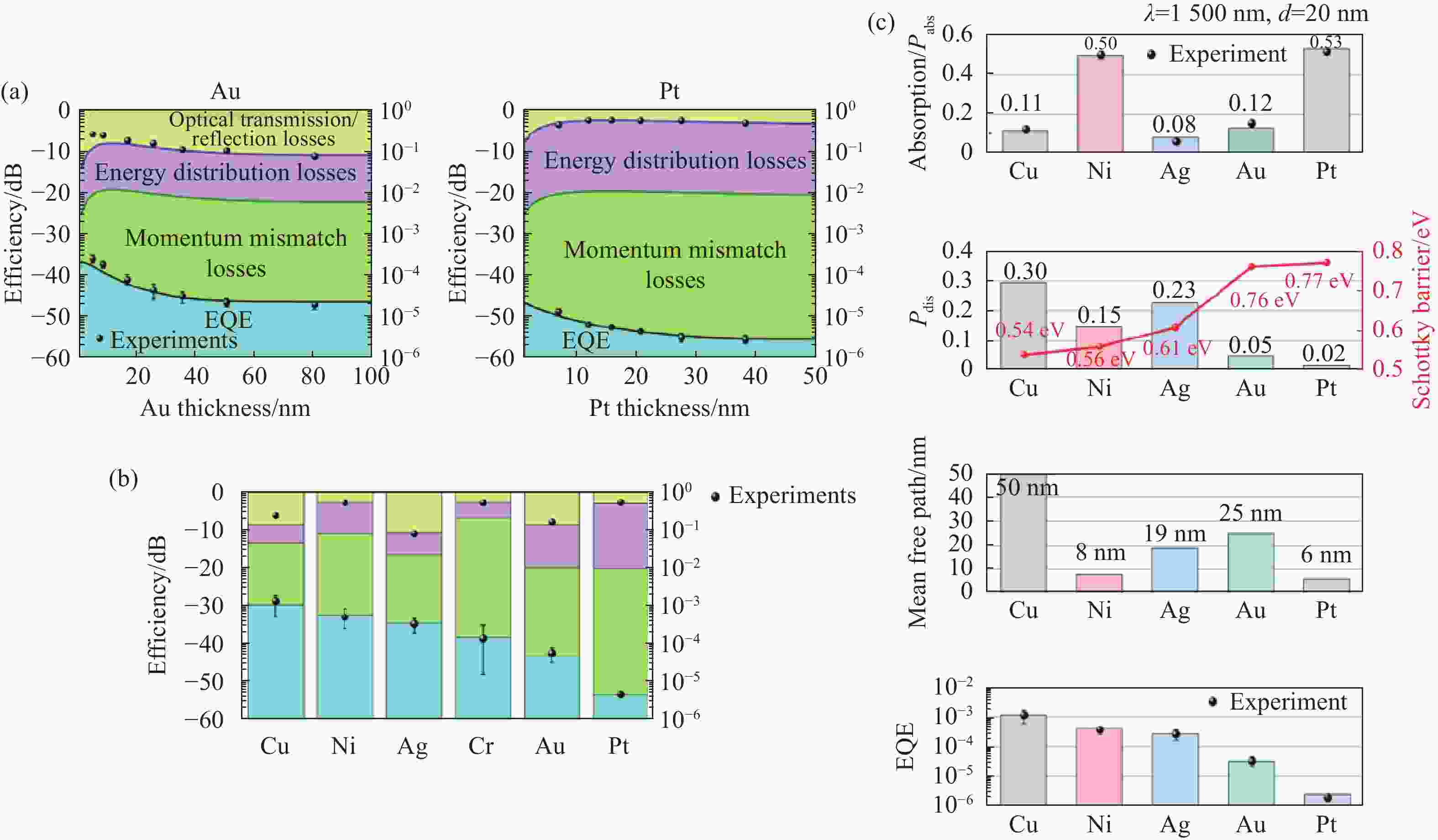
图 12 (a) Au和Pt肖特基探测器在1510 nm波长下的三种主要热电子损耗机制占比;(b)定量比较了20 nm厚度的六种金属肖特基探测器的外量子效率;(c) Cu,Ni,Ag,Au,Pt 五种金属对应得吸收率,注入概率,平均自由程以及量子效率
Figure 12. (a) The proportion of three main thermoelectronic loss mechanisms of Au and Pt Schottky detectors at 1510 nm; (b) Quantitative comparison of the external quantum efficiency of six metal Schottky detectors with a thickness of 20 nm; (c) The five metals Cu, Ni, Ag, Au, Pt pair absorption rate, injection probability, mean free path and quantum efficiency
最近,Seok等基于Cu,Ni,Ag,Au,Pt五种不同金属的热电子探测器的光吸收率,注入概率,平均自由程以及量子效率进行了详细对比[63],如图12(c)所示。发现基于铜的探测器虽然吸收率不高,但是注入概率和平均自由程都最大,使得其量子效率达到了最高。另外,还发现当将铜的厚度从40 nm减小到8 nm时,相应的外量子效率值增加了4倍以上。这些结果也说明热电子平均自由程和金属膜的厚度对于光电转化效率具有重要的影响。
-
热电子产生后的初始能量决定了其是否具有足够的能量越过肖特基势垒,所以它对光电转化效率起着关键作用。热电子能量除了受激发光子的能量的影响外,还与材料本身的态密度等因素相关,这为优化热电子的能量分布提供了可能。另一方面,热电子初始动量方向决定了其运动的方向,实际中期望热电子朝着肖特基界面方向运动,因此初始动量分布也会影响热电子到达肖特基界面的概率。
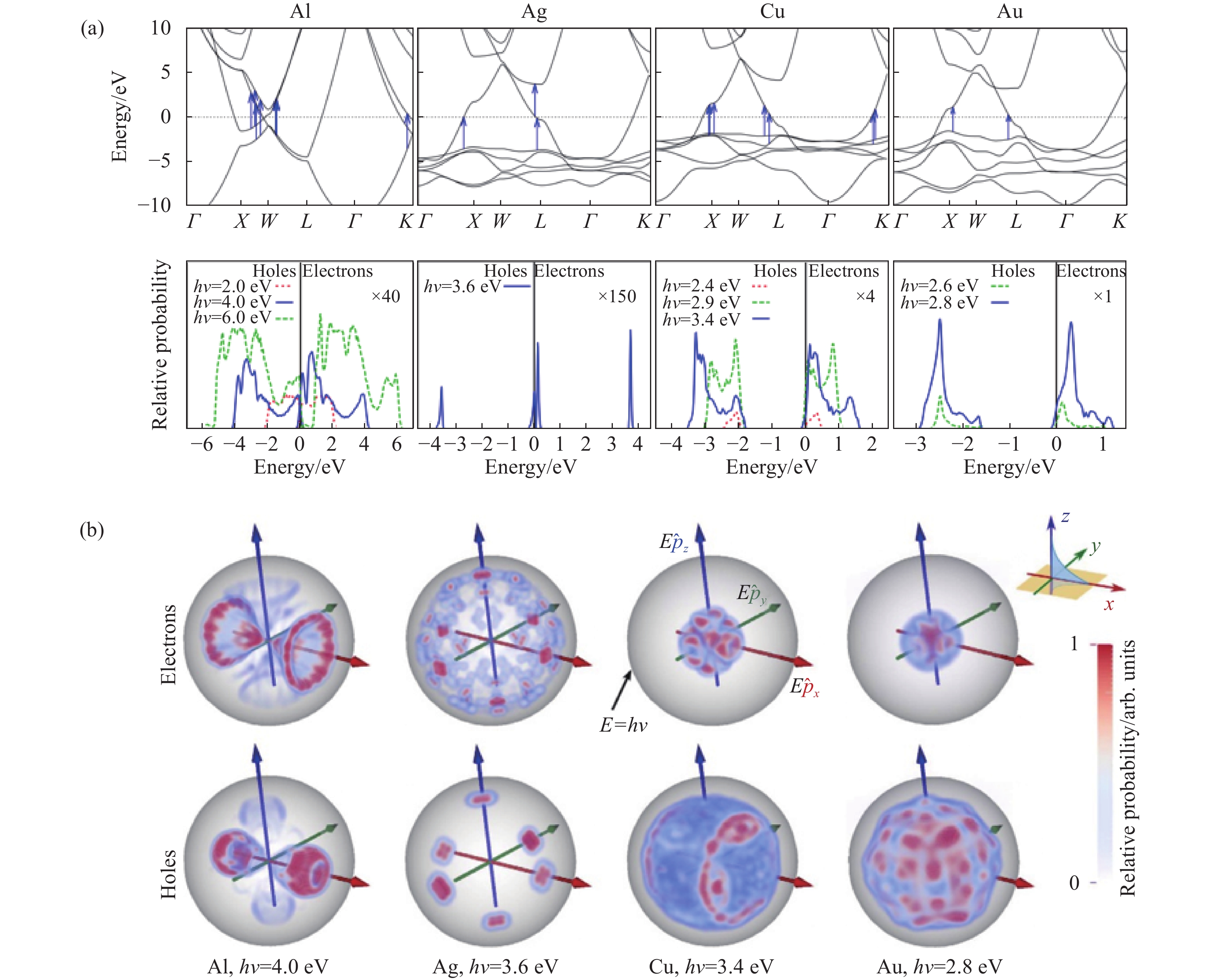
2014 年,Sundararaman等基于第一性原理计算方法,对铝、金、银和铜中等离激元产生的热载流子初始能量和动量进行了对比分析,发现产生的热载流子能量与电子能带结构密切相关,特别是d带离费米能级的距离[17]。如图13所示,铜与金由于更容易激发高能量热空穴和低能量电子,银产生的热空穴和热电子的能量分布较窄,而铝则产生空穴和电子的连续能量分布。他们还发现金属的尺度减小到纳米级后,几何辅助带内跃迁也可以使铜和金中产生能量较高的热电子。另外,热载流子的动量分布与金属的晶向和等离激元极化方向密切相关,但都不是均匀的,这点与Fowler模型的动量均匀性假设不同。
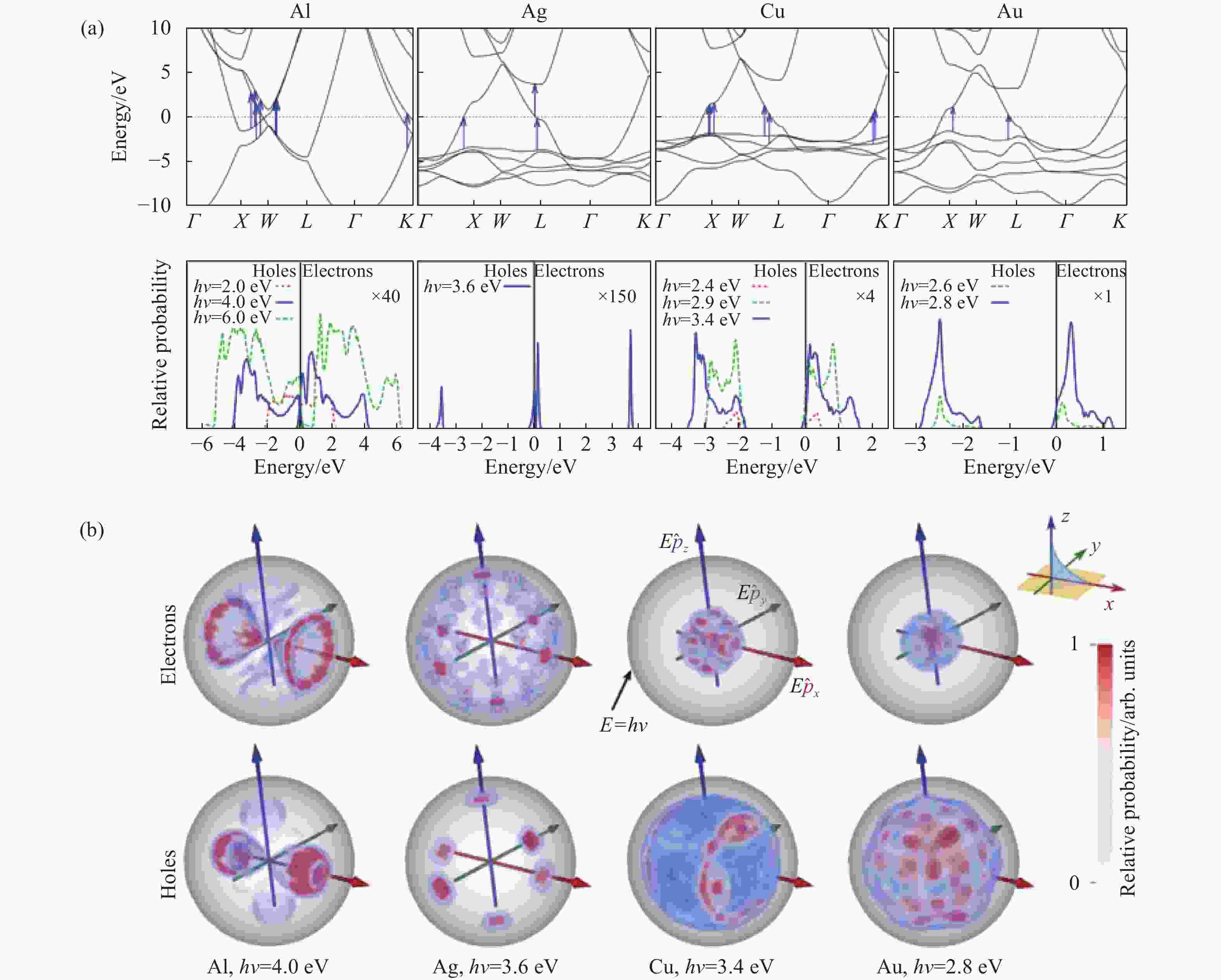
图 13 (a)从左到右依次是铝、银、铜和金的能带结构和热载流子能量分布与入射光子能量的关系(上图为热电子可能发生的跃迁在能带中的位置,下图为热载流子的能量分布); (b)从左到右依次是铝、银、铜和金的能量和动量方向分布(上图为热电子的能量和动量方向分布,下图为空穴能量和动量方向分布)
Figure 13. (a) From left to right, the band structure of aluminum, silver, copper and gold and the relationship between the hot carrier energy distribution and the incident photon energy are shown (The above figure shows the position of the possible transition of hot electrons in the energy band, and the following figure shows the energy distribution of hot carriers); (b) From left to right are the directional distributions of energy and momentum for aluminum, silver, copper and gold (The above figure shows the direction distribution of energy and momentum of hot electrons, and the following figure shows the direction distribution of energy and momentum of holes)
2015年,Bernardi等人运用密度泛函理论和多体格林函数方法,深入探究了金和银中表面等离子体激元所引发的热电子能量分布及其散射机制。研究结果显示,等离子体激元在衰变为热电子的过程中,主要存在两种截然不同的过程:带内过程与带间过程[64]。在带内过程中,热电子的能量分布均匀,能量水平相对较高,同时它们的平均自由程也较大;而带间过程则表现出不同的特点,其中热电子的能量较低,热空穴的能量则相对较高,并且热电子的平均自由程相对较小。Gong等对一系列金属和合金材料的热载流子分布进行了理论计算,发现热载流子的初始能量和动量分布由材料类型和入射光的能量共同决定[65]。
同年,Brown等采用第一性原理计算方法,并通过该计算预测了四种不同金属产生热电子的初始能量分布,发现由于声子辅助跃迁和直接跃迁所引起金属的热载流子初始能量分布是有所不同[38]。等离激元衰变能量在高于带间阈值,直接跃迁占主导地位,相应的热载流子初始能量分布取决于等离子体金属;而低于带间阈值时,声子辅助跃迁产生从零到等离子体激元能量的均匀热载流子能量分布。该结论与先前的研究基本一致。
-
成功到达肖特基界面的热电子要注入到硅中,还需满足其垂直于肖特基界面的动能分量高于肖特基势垒高度的条件。这意味着对于具备特定动能的热电子,仅当其运动方向处于一个锥形区域内时,才能有效实现注入。为了提高热电子的注入概率,研究者也发展出了多种方法,包括增加肖特基界面的面积、调控界面的性质等。
-
采用多个肖特基结的设计可以增加肖特基界面的面积,从而使得更多运动方向的热电子都能够满足注入的条件。
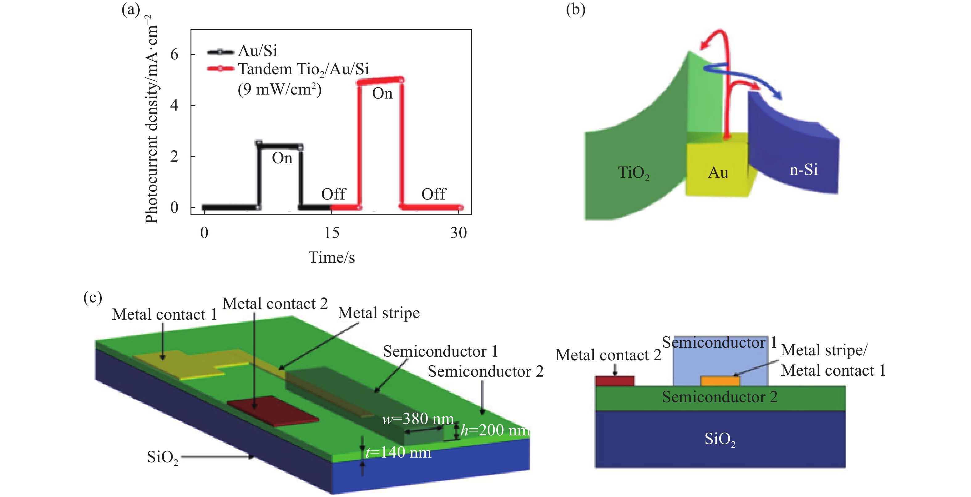
2013 年,Knight等将等离子微纳结构嵌入到硅中,形成了三个肖特基界面,这种嵌入方法使得热电子探测器的响应度提高了25倍[66]。2014 年,Lee等设计并制备了TiO2/Au/Si双肖特基串联结构的热电子器件[67]。如图14 (a)、 (b)所示,相比于单层肖特基器件,其提高了约50%。这是由于双肖特基势垒为收集热电子提供了额外的途径,通过两个势垒之间不同能量范围的多重反射,使热电子的收集得到了增强。
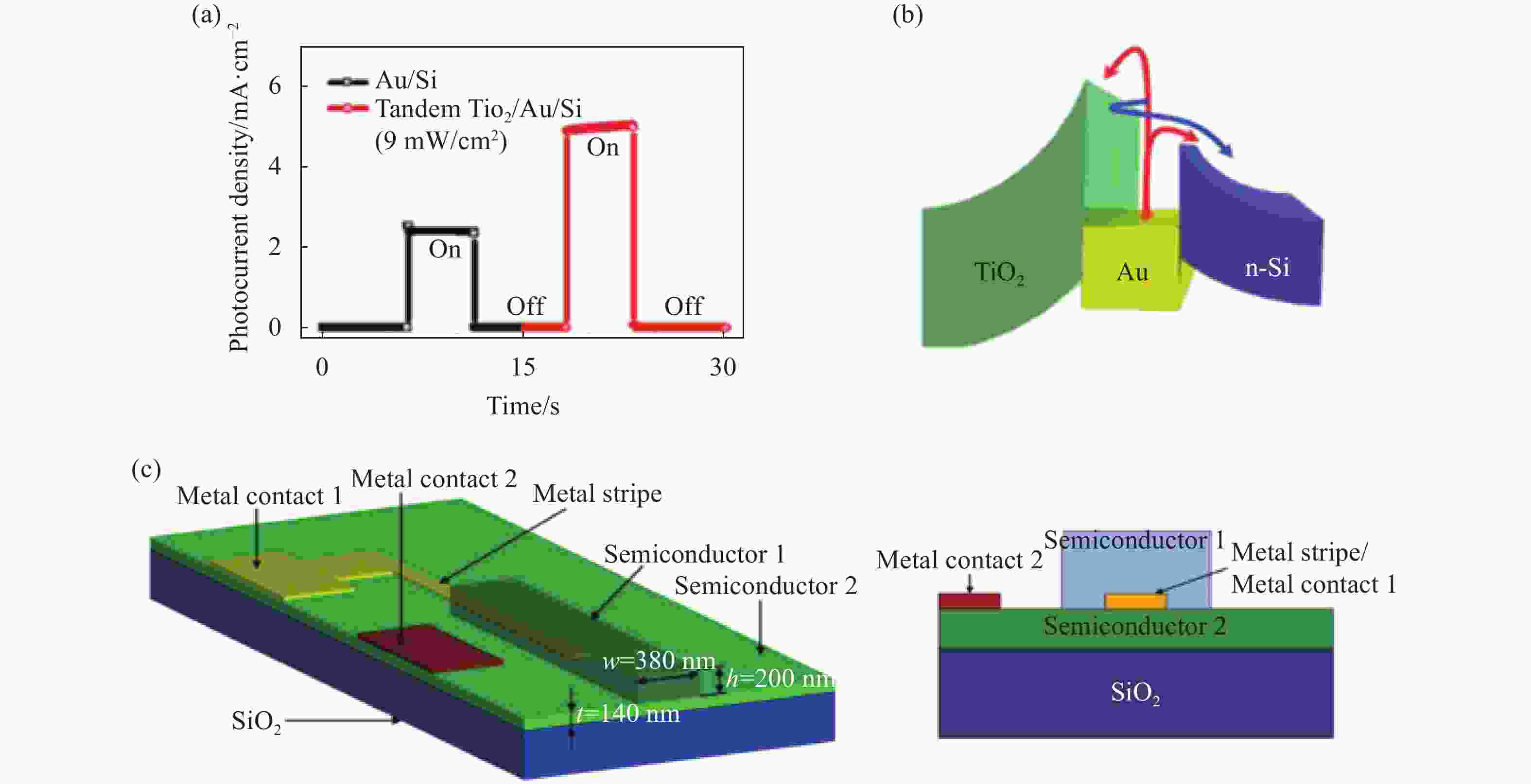
图 14 (a)铝、(b) 银、(c) 铜和 (d)金的能带结构和热载流子能量分布与入射光子能量的关系(其中,上图为热电子可能发生的跃迁在能带中的位置,下图为热载流子的能量分布)
Figure 14. The relationship between the energy distribution of (a) aluminum, (b) silver, (c) copper and (d) gold and the energy of incident photons(Among them, the above figure shows the position of the possible transition of hot electrons in the energy band, and the following figure shows the energy distribution of hot carriers)
2019年,Gosciniak等人提出了一种波导集成型肖特基热电子探测器设计方案[21],该方案显著特点在于将金属条带完整嵌入半导体材料之中,其结构示意如图14(c)所示。由于金属条带被半导体完全包裹,所有具备适宜波矢的热电子均能顺利注入硅中,从而显著提升热电子注入效率。作者预测该器件响应度在1550 nm处可达0.5 A/W。此外,苏州大学的李孝峰团队借助蒙特卡洛模拟方法,研究了热电子器件的注入效率,对比分析了单肖特基和双肖特基器件的注入效率[42]。研究结果显示,在较厚的金属层中,双结系统的热电子注入效率(达到1.07%)显著高于单结系统(仅为0.64%)。然而,在金属层较薄的情况下,两者的效率则较为接近。这一发现表明,当金属厚度较大时,双结系统在热电子注入效率方面展现出显著的优势;而在金属较薄时,两者的效率则趋于接近。这一理论模型的建立,不仅为双肖特基探测器结构的设计提供了理论依据,也为多肖特基探测器结构的进一步研究和优化提供了重要的指导。
-
研究者们发现肖特基界面的性质,如引入其他材料可以调控热电子的注入概率。例如,2016年Goykhman等发现,通过在片上集成的金-硅热电子探测器中引入石墨烯,可以有效弥补两者之间的晶格缺陷,促进热电子的注入。该探测器的响应度在1550 nm处高达85 mA/W,同时其内量子效率也达到了7%,相较于传统的金属-硅肖特性能提升了一个数量级[68]。除此之外,2019年Güsken等P型硅与TiN薄膜涂层之间形成的非晶TiO2−x薄膜具有丰富的陷阱态,可以显著提高热电子探测器的响应度[69]。基于该结构,可使Au/TiO2−x/p-Si探测器在1250 nm处的响应度提升至4 mA/W,如图15 (a)所示。
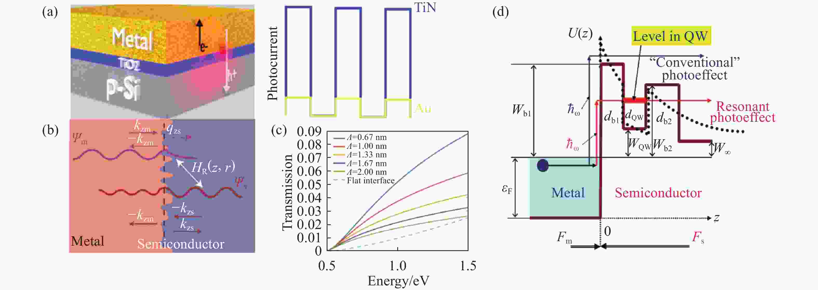
图 15 (a)金属/TiO2−x/p-Si探测器结构及对光电响应的提升效果; (b)粗糙界面示意图;(c)在金属半导体界面的不同粗糙度下,热电子注入概率与电子能量的关系,Λ越小表示粗糙度越大;(d)金属-半导体结引入量子阱后的能带图。虚线为肖特基势垒,量子阱中的准离散能级用红色粗线表示
Figure 15. (a) Metal/TiO2−x/p-Si detector structure and its effect on photoelectric response; (b) Rough interface diagram; (c) The relationship between the probability of hot electron injection and electron energy under different roughness of metal semiconductor interface, the smaller Λ indicates the larger roughness. (d) Band diagram of metal-semiconductor junction after introduction of quantum well. The dashed line is the Schottky barrier, and the quasi-discrete energy levels in the quantum well are represented by the thick red line
此外,调整肖特基界面的粗糙度同样可以有效提升热电子的注入概率。2012年,Levy研究团队利用与CMOS兼容的硅局部氧化方法,成功研制出了一种低损耗波导型热电子探测器[70]。该探测器在1550 nm的工作波长下,响应度高达12.5 mA/W,内量子效率也达到了1%。这一性能的实现主要归功于制造工艺所引发的粗糙界面,其不仅能够在尖锐边缘处形成局部高强度电场,还能够打破界面处电子注入的动量守恒规则。因此,原本可能会完全反射回金属的热电子,得以顺利进入硅中,从而显著提高了热电子的注入效率。随后,Khurgin等对此进行了深入地探究,分析了热电子注入概率与肖特基界面的粗糙度的关系[71],如图15 (b)、(c)所示。他们对比了不同粗糙度下热电子的注入概率,发现界面的粗糙度越高(即图中Λ越大),电子注入概率越高。热电子注入概率的提高是由于粗糙界面可以等效为电子随机光栅,增加了热电子注入到硅中的动量方向的范围,从而提升注入概率。该团队后来又提出在金属-半导体界面引入量子阱,形成准离散能级,利用电子共振隧穿的方法可大幅提高热电子的注入概率[72],如图15(d)所示。复旦大学Feng等人发现将金-硅肖特基结的硅制成纳米线,可以增加硅的态密度,基于该方法也可提高热电子注入概率 [73],如图16所示。在1150 nm处,其响应度达到了94.5 mA/W, 比探测率达到了4.38×1011cm·Hz0.5/W。
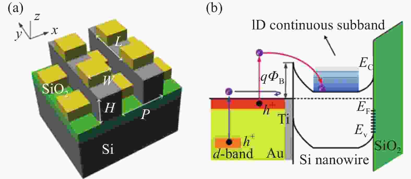
图 16 (a)金-硅肖特基结的硅制成纳米线结构; (b)硅纳米线/金天线界面中的能带结构示意图
Figure 16. (a) Nanowire structures made of silicon with gold-silicon Schottky junction; (b) Schematic diagram of band structure at the silicon nanowire/gold antenna interface
-
在上一节中,讨论了提升硅基热电子光电转化效率的策略,这些策略在实质上是提升了探测器的响应度或量子效率。然而,要全面评估探测器的性能,除了响应度和量子效率之外,比探测率和等效噪声功率同样不可忽视,因为它们能够更全面地反映探测器的信噪比表现。为了获得更高的比探测率(或实现更低的等效噪声功率),探测器不仅需要维持高响应度,还必须实现低暗电流。值得注意的是,肖特基探测器由于其电荷传输机制主要依赖于多数载流子,其暗电流水平往往高于PN结等依赖少数载流子传输的器件。因此,有效降低肖特基热电子探测器的暗电流成为了一项值得深入研究的课题。
首先,通过减小金属与半导体接触面积可减小暗电流。例如,Wen等设计了金字塔型探测器结构,通过金字塔结构中实施部分金属化,显著减少了金属与半导体之接触界面[34]。这一设计不仅成功将热电子聚焦于纳米尖端,还有效地将暗电流降低了两倍,显著提升了探测器的性能。
其次,通过界面调控也可以抑制暗电流。例如,Kim等通过石墨烯/锗肖特基结探测器的界面引入了一层很薄的氧化铝层,可增加低能载流子的隧穿距离并减少界面处的费米能级钉扎效应,从而抑制了暗电流[74]。测试发现,基于该方法暗电流可降低两个数量级。Yang等通过在石墨烯/硅肖特基结探测器的界面引入一层钆铁石榴石(Gd3Fe5O12,GdIG)薄膜[75],可有效钝化接触界面并增加势垒高度,实现了对暗电流的抑制。在施加−2 V的偏压条件下,该结构的暗电流显著降低了54倍;同时在自供电模式下,其开关比达到了的8.2 × 10⁶。
此外,提高肖特基势垒高度也是抑制暗电流的有效手段。2018年,厦门大学Huang等通过在ITO与硅之间引入极薄的银层,并将银退火成纳米颗粒,发现可将肖特基势垒高度提高0.32 eV,进而可将暗电流降低2300倍[76]。2020年,中国科学院物理研究所Li等人基于类似的思路,在ITO与硅之间引入极薄的金层以提高肖特基势垒高度,发现器件的暗电流可以低至10−7A/cm2,同时探测器的整流比可达1.5×108[43]。随后,Lee等通过在石墨烯中掺杂聚乙烯亚胺,成功地将石墨烯/p型硅光电探测器的肖特基势垒高度从0.42 eV调制至0.68 eV[77]。这一方法显著改善了探测器的性能,使暗电流从980 nA大幅降低至219 pA。与未掺杂的器件相比,暗电流降低了4000倍。
值得注意的是,在调控肖特基热电子探测器的暗电流时,常常会伴随着对光电转化效率的影响。因此,需要考虑比探测率或等效噪声功率这类衡量信噪比的综合指标,以确保对探测器性能优化程度的准确评估。
-
综上所述,硅基热电子短波红外探测技术近年来取得了显著进展,表1详尽地总结了代表性硅基热电子探测器的性能。这些探测器响应度通常在mA/W的量级,暗电流一般在10−4~10−8 A/cm²的范围内,对应的比探测率在106~1010 Jones的区间。值得注意的是,部分采用创新结构设计的硅基热电子器件展现出了更为卓越的性能,例如Feng等人提出的一种基于超表面天线结构的器件[73],其比探测率达到了1011 Jones的量级,这说明硅基热电子探测器在性能提升方面仍然具有潜力。
表 1 近年来硅基热电子短波红外探测器汇总
Table 1. Summary of silicon-based hot electron shortwave infrared detectors in recent years
Device type/
Enhancement strategyResponsivity Dark current/
Dark current densityDetectivity/
JonesNEP/
W·Hz−1/2Year Au film on Si nanobowl[35]
Hot electron generation0.34 mA·W−1@1300 nm
0.29 mA·W−1@1500 nm2.5×10−7 A None 8.3×10⁻¹⁰ 2021 Disordered Au/
Si nanoneedles[50]
Hot electron generation2.56 mA·W−1@1300 nm
0.33 mA·W−1@1500 nm4×10−10 A None 4.4×10⁻¹²
@1300 nm2023 Au antennas/Ti/Si[51]
Hot electron generation10 μA·W−1@1250 nm
3 μA·W−1@1550 nmNone None None 2011 Deep-trench/thin Au/
Si antenna[52]
Hot electron generation3 mA·W−1@1300 nm
1.25 mA·W−1@1400 nm
0.5 mA·W−1@1550 nm8.7×10−9 A·cm−2 5.68 ×10¹⁰
2.37 ×10¹⁰
9.47 ×10⁹None 2014 Metamaterial Au/Si[53]
Hot electron generation3 mA·W−1@1300 nm None None None 2014 Two distributed Bragg reflectors (DBRs)
Al2O3/TiO2 Al2O3/TiO2/Au[54]
Hot electron generation27 mA·W−1@813 nm None None None 2021 Disordered Au Si NHs[55]
Hot electron generation1.5-13 mA·W−1
@1100-1500 nm1×10−6 A None 4.75×10⁻¹¹-
3.77×10−102018 Au grating/Si[16]
Hot electron generation0.6 mA·W−1@1460 nm None None None 2013 Material-embedded
Trenchlike thin Au/Si[61]
Hot electron generation5854 nA·mW−1@1310 nm
693 nA·mW−1@1550 nmNone None None 2019 Au/Si pyramid [22]
Hot electron generation5.2 mA·W−1@1200 nm None None None 2020 Au NWs embedded in Si[66]
Hot electron injection0.065 mA·W−1@1500 nm 1×10⁻⁹ A 3.63×10⁶ 2.75×10⁻¹⁰ 2013 TiN/thin Au stripe
embedded in Si[68]
Hot electron injectionExceed 1.0 A·W−1@1550 nm None None None 2016 Thin film TiN/p-Si[69]
Hot electron injection1 mA·W−1@1250 nm 3×10⁻¹⁰ A 6.12×10⁸ 9.8×10⁻¹² 2019 Waveguide-based Al/Si[70]
Hot electron injection12.5 mA·W−1
@1550 nm (0.1 V)3×10⁻⁸ A
(0.1 V)None 7.84×10⁻¹² 2012 Metasurface Au/Si[73]
Hot electron transfer
and injection94.5 mA·W−1
@1150 nm (1.5 V)1.45×10⁻⁷
A·cm−24.38 ×10¹¹ None 2019 Partially metalizing the
pyramid Al/SiO2/Si[34]
Dark current suppressionNone Reduce by
2 timesNone None 2021 Graphene/Al2O3/Ge[74]
Dark current suppression1.2 A·W−1@1550 nm (2 V) 1×10⁻⁶ A None None 2021 Interface engineering
assisted graphene/Si[75]
Dark current suppressionNone@890 nm 7.2×10⁻¹⁰ A 9.3×10¹² 1.8×10⁻¹² 2022 ITO/ Thin Ag/n-Si[76]
Dark current suppression0.05 A·W−1@1550 nm (2 V) 2.4×10⁻⁶
A/cm2 (−1 V)None None 2018 Thin ITO/Au/
Au Nanoparticle/n-Si[43]
Dark current suppression2.82 mA·W−1@1310 nm
(−1 V)4.4×10⁻⁵
A/cm2 (−1 V)None None 2022 Graphene with
polyethyleneimine/p-Si[77]
Dark current suppression0.3 A·W−1@850 nm 2.4×10⁻¹⁰ A 5.9×10¹⁰ None 2021 NanoalloysAu40Ag60/Si[78]
Hot electron transfer7.3 mA·W−1@1310 nm
1.9 mA·W−1@1550 nmNone None None 2024 Au/crystallized Ge/Si[79]
Hot electron injection0.71 A·W−1@1310 nm
0.64 A·W−1@1550 nm (1 V)None None None 2022 TalrTe4/Si[80]
Hot electron transfer14 mA·W−1@1310 nm
1.32 mA·W−1@1550 nmNone None None 2022 Mo2C/MoGeSiN4/Si[81]
Hot electron transfer176 mA·W−1@1550 nm None None None 2022 尽管硅基热电子探测器在兼容CMOS制造工艺和成本效益方面具有显著优势,但与铟镓砷、锗、量子点等传统短波红外探测器相比,商用铟镓砷光电探测器具备高响应度,通常达到A/cm2的量级,同时暗电流保持在10−9 A/W的级别,其比探测率普遍在1012~1014 Jones范围内。同样,锗和量子点短波红外探测器在响应度、暗电流和比探测率等方面均表现出与铟镓砷探测器相近的性能。
展望未来,硅基热电子短波红外探测技术的发展仍具有广阔的前景。通过不断优化器件结构、提高材料性能以及探索新的机制,有望进一步提升硅基热电子探测器的性能,缩小与传统短波红外探测器之间的性能差距。具体而言,可从以下几个方面进一步开展研究:
1)在新材料研究方面,可开发性能更为卓越的热电子材料。重点分析材料的热电子自由程和电子态密度两个核心属性,它们对硅基热电子探测器的光电转换效率有着显著的影响。一方面,平均自由程越长,热电子越容易穿越材料内部并成功注入到肖特基界面,从而提升光电转换效率。另一方面,材料的电子态密度亦至关重要,它决定了热电子的初始能量分布。理想情况下,期望材料在费米能级附近表现出很高的电子态密度,这样电子在受到光子激发时,更可能形成高能量的电子,进而进一步提升光电转换效率。为了获得上述材料性质,可考虑探索金属合金材料[78]、导电氧化物、金属硅化物、金属氮化物和新型二维材料等,这些材料可能提供优化热电子发射性能的新途径[79−80],推动硅基热电子短波红外探测器性能的进一步提升。
2)在新结构研究方面,需解决两个重要的问题。首先是如何通过创新的微纳结构设计,实现宽带宽红外光的高效吸收。尽管当前在提升探测器吸收率方面的工作已经较为丰富,且吸收率也能达到较高水平,但如何在保证宽带宽的同时实现高吸收率,仍然是一个具有挑战性的任务。其次,需深入探索肖特基界面结构与其性质之间的关系。肖特基界面的特性不仅直接关系到热电子的注入效率,还会对探测器的暗电流产生显著影响。因此,如何精心设计界面结构,例如通过引入二维材料、调控界面表面态和粗糙度等手段,提升热电子注入效率,同时保持或降低暗电流水平,也是值得深入研究的课题。
3)在新机制研究方面,可探索更高效的光电转换原理,以突破当前硅基热电子探测器的性能瓶颈。目前,多数报道的硅基热电子探测器遵循着热电子产生、传输和注入的经典理论框架。然而,在这一框架下的每一个环节,均存在多个热电子能量的损耗路径,这难以避免地导致了光电转换效率的低下。因此,需寻求改变这种经典光电转换机制。例如,近期有报道指出,热电子在受到光激发后能够直接从金属跃迁到硅材料中,这种直接且高效的过程有望显著提升光电转换效率[82−83]。此外,还可以借鉴近年来在半金属二维材料中发现的热电子的光热电效应等新型机制[84−91]。这些探索可能会从根本上突破现有原理的限制,为未来的红外探测技术发展开辟新的路径。
总之,硅基热电子探测技术能够将硅的响应波段拓展至短波红外波段,同时与硅基半导体工艺兼容,具有低成本和高均一性等优势,有望在军事、安防、环境监测等多个领域发挥重要的作用。文中从肖特基热电子探测技术的光电转换机制出发,对热电子的产生、传输及注入三个核心环节进行系统回顾。并针对上述三个环节所存在的能量损耗过程分析了相应的应对措施或优化策略。此外,也探讨了暗电流的抑制方法,为硅基热电子短波红外探测器的进一步优化与应用提供参考。
Silicon based hot electron short wave infrared detection technology (cover paper·invited)
-
摘要: 短波红外具有穿透烟雾的特性,可在低光照环境或恶劣天气条件下成像,在军事、安防、环境监测等多个领域展现出重要应用价值。硅基热电子短波红外探测技术因具备与CMOS半导体工艺兼容、响应波段灵活可调等独特优势,已成为当前研究的热点。文中系统地回顾了该领域的国内外研究进展,剖析了与光电转换效率密切相关的热电子产生、传输与注入等物理过程中的能量损耗机制。在此基础上,总结了针对性的改进策略,包括通过光学吸收增强和热损耗抑制来增加热电子的产生效率;通过精确调控热电子的初始位置、能量、动量分布及自由程来优化其传输过程;以及利用肖特基结和界面调控等技术来提高热电子的注入概率。此外,文中还讨论了暗电流的抑制方法,以期提升探测器的整体性能。最后,展望了硅基热电子红外光电探测器未来的发展方向。Abstract:
Significance Short wave infrared detectors, as a very important type of detector, play a crucial role in sensing and obtaining target image information. Their notable features include the ability to penetrate smoke, high spatial recognition, all-weather working ability, and applicability in harsh weather conditions, making it widely applicable in multiple fields of national major needs and national economic development. In the military field, shortwave infrared detectors, with their unique night vision and covert reconnaissance functions, have become a key tool for enhancing combat capabilities at night and in adverse weather conditions. In the field of security monitoring, it provides strong technical support for video monitoring under low or no light conditions, significantly enhancing security capabilities. In terms of environmental monitoring, these detectors provide valuable data support for environmental protection and climate research by accurately measuring specific components in the atmosphere. In addition, in the medical field, the application of shortwave infrared detectors in disease diagnosis has opened up new paths for medical technology innovation. Therefore, in-depth research on shortwave infrared detectors has important practical significance. Progress This article systematically reviews the photoelectric conversion mechanism of Schottky photodetector, and summarizes and analyzes recent research results at home and abroad around the basic physical processes of hot electrons. This article first introduces the formation and basic characteristics of metal silicon Schottky junctions, and explores the three core processes of hot electron generation, transmission, and injection. Next, in terms of the generation of hot electrons, a review is conducted on the relevant work of researchers to improve the efficiency of hot electron generation through methods such as light absorption enhancement and thermal loss suppression. In terms of the transfer of hot electrons, the current proposed methods to control the initial position, initial energy and momentum, and mean-free path of hot electrons have been summarized to improve the transfer efficiency of hot electrons. In the injection method of hot electrons, strategies to improve injection efficiency such as multiple Schottky junctions and interface engineering were introduced. In addition, considering the crucial impact of dark current on detector performance, this article also explores current methods for suppressing dark current. Finally, this article provides an outlook on the future development direction of this field. Conclusions and Prospects Silicon-based hot electron detection technology holds the potential to broaden the response band of silicon to include the short-wave infrared band, while maintaining compatibility with silicon-based semiconductor processes. Its advantages, including low cost and high uniformity, bode well for its significant role in diverse fields such as military applications, security, and environmental monitoring. Looking ahead, it is imperative to delve deeper into the research of novel materials, structures, and mechanisms to further enhance the detector's performance. By focusing on developing new materials that can enhance the mean-free path of electrons and optimize the density of states, the transport efficiency of hot electrons can be boosted. Concurrently, the pursuit of innovative structures that efficiently absorb wide-spectrum infrared light, coupled with the optimization of the Schottky interface to increase hot electron injection efficiency and minimize dark current, is paramount. Moreover, exploring novel photoelectric conversion mechanisms that transcend the constraints of classical frameworks offers a promising avenue for pioneering advancements in infrared detection technology. -
Key words:
- short wave infrared /
- hot electrons /
- detector /
- Schottky junction
-
图 1 金属-硅肖特基结形成的原理示意图。 (a)金属和硅接触前的能带图; (b)金属和N型硅接触后的肖特基结能带图;(c)金属和P型硅接触后的肖特基结能带图;(d)肖特基结的典型电流-电压特性曲线
Figure 1. Schematic diagram of the formation principle of metal-silicon Schottky junction. (a) Energy band diagram before the contact between metal and silicon; (b) Energy band diagram of Schottky junction after the contact between metal and N-type silicon; (c) Energy band diagram of Schottky junction after the contact between metal and P-type silicon; (d) Typical current-voltage characteristic curve of Schottky junction
图 2 热电子产生、传输和注入三个阶段中能量的传递和损耗过程
Figure 2. The process of energy transfer and loss in the three stages of hot electron generation, transport, and injection
图 3 金属材料类型对热电子初始能量分布的影响
Figure 3. Effect of metal material type on initial energy distribution of hot electrons
图 4 (a)热电子受到的散射过程及时间尺度; (b)热电子受电子和声子散射的平均自由程与热电子能量的关系
Figure 4. (a) The scattering process and time scale of hot electrons; (b) the relationship between the mean free path of hot electrons scattered by electrons and phonons and the energy of hot electron
图 5 能够注入到硅中的热电子动量的锥形分布
Figure 5. The conical distribution of the momentum of hot electrons that can be injected into silicon
图 6 (a)、(b)基于一维和二维超材料完美吸收器的光电探测器示意图;(b)、(c)和(e)、(f)分别为(a)和(b)图探测器对应的吸收和响应曲线
Figure 6. (a), (b) Schematic diagram of a photodetector based on a one - and two-dimensional metamaterial perfect absorber; (b), (c) and (e), (f) are the absorption and response curves corresponding to the detectors in figure (a) and (b), respectively
图 7 (a) Tamm等离激元增强型热电子探测器结构示意图; (b)其与光栅耦合增强型热电子探测器的响应度对比图
Figure 7. (a) Schematic diagram of the Tamm plasmon enhanced thermal electron detector; (b) Comparison diagram of its responsiveness with the grating coupled enhanced thermionic detector
图 8 (a)随机结构增强热电子探测器示意图;(b)不同退火温度下制备的Au/SiNH结构的吸收光谱;(c)不同Au涂层厚度的Au/SiNH器件的响应度;(d)不同照明模式下的响应度;(e)不同温度退火制备的Au/SiNH的扫描电镜(SEM)图像
Figure 8. (a) Schematic diagram of a random structure enhanced thermionic detector; (b) Absorption spectra of Au/SiNH structures prepared at different annealing temperatures; (c) The responsiveness of Au/SiNH devices with different Au coating thicknesses; (d) Responsiveness under different lighting modes; (e) Scanning electron microscopy (SEM) images of Au/SiNH prepared by annealing at different temperatures
图 9 (a)半无限表面、 (b) 40 nm、(c) 20 nm和(d) 10 nm直径球体中的热损耗、几何辅助、声子辅助和直接跃迁占吸收总能量的百分比随频率变化的关系
Figure 9. The frequency variation of the percentage of heat loss, geometrical assist, phonon assist and direct transition to the total absorbed energy in (a) semi-infinite surface, (b) 40 nm, (c) 20 nm and (d) 10 nm diameter spheres
图 10 (a)银纳米棒阵列探测器结构图;(b)该探测器中热电子产生的初始位置
Figure 10. (a) Structure diagram of silver nanorod array detector; (b) The initial position of hot electron generation in the detector
图 11 (a)沟槽式天线结构探测器在正照式(左)背照式(右)探测示意图;(b) 金-硅微锥结构探测器中正面和背面照射模式下的响应率曲线
Figure 11. (a) The channel antenna structure detector in the front light (left) back light (right) detection diagram; (b) Response curves of gold-silicon microcone detectors in front and back irradiation modes
图 12 (a) Au和Pt肖特基探测器在1510 nm波长下的三种主要热电子损耗机制占比;(b)定量比较了20 nm厚度的六种金属肖特基探测器的外量子效率;(c) Cu,Ni,Ag,Au,Pt 五种金属对应得吸收率,注入概率,平均自由程以及量子效率
Figure 12. (a) The proportion of three main thermoelectronic loss mechanisms of Au and Pt Schottky detectors at 1510 nm; (b) Quantitative comparison of the external quantum efficiency of six metal Schottky detectors with a thickness of 20 nm; (c) The five metals Cu, Ni, Ag, Au, Pt pair absorption rate, injection probability, mean free path and quantum efficiency
图 13 (a)从左到右依次是铝、银、铜和金的能带结构和热载流子能量分布与入射光子能量的关系(上图为热电子可能发生的跃迁在能带中的位置,下图为热载流子的能量分布); (b)从左到右依次是铝、银、铜和金的能量和动量方向分布(上图为热电子的能量和动量方向分布,下图为空穴能量和动量方向分布)
Figure 13. (a) From left to right, the band structure of aluminum, silver, copper and gold and the relationship between the hot carrier energy distribution and the incident photon energy are shown (The above figure shows the position of the possible transition of hot electrons in the energy band, and the following figure shows the energy distribution of hot carriers); (b) From left to right are the directional distributions of energy and momentum for aluminum, silver, copper and gold (The above figure shows the direction distribution of energy and momentum of hot electrons, and the following figure shows the direction distribution of energy and momentum of holes)
图 14 (a)铝、(b) 银、(c) 铜和 (d)金的能带结构和热载流子能量分布与入射光子能量的关系(其中,上图为热电子可能发生的跃迁在能带中的位置,下图为热载流子的能量分布)
Figure 14. The relationship between the energy distribution of (a) aluminum, (b) silver, (c) copper and (d) gold and the energy of incident photons(Among them, the above figure shows the position of the possible transition of hot electrons in the energy band, and the following figure shows the energy distribution of hot carriers)
图 15 (a)金属/TiO2−x/p-Si探测器结构及对光电响应的提升效果; (b)粗糙界面示意图;(c)在金属半导体界面的不同粗糙度下,热电子注入概率与电子能量的关系,Λ越小表示粗糙度越大;(d)金属-半导体结引入量子阱后的能带图。虚线为肖特基势垒,量子阱中的准离散能级用红色粗线表示
Figure 15. (a) Metal/TiO2−x/p-Si detector structure and its effect on photoelectric response; (b) Rough interface diagram; (c) The relationship between the probability of hot electron injection and electron energy under different roughness of metal semiconductor interface, the smaller Λ indicates the larger roughness. (d) Band diagram of metal-semiconductor junction after introduction of quantum well. The dashed line is the Schottky barrier, and the quasi-discrete energy levels in the quantum well are represented by the thick red line
图 16 (a)金-硅肖特基结的硅制成纳米线结构; (b)硅纳米线/金天线界面中的能带结构示意图
Figure 16. (a) Nanowire structures made of silicon with gold-silicon Schottky junction; (b) Schematic diagram of band structure at the silicon nanowire/gold antenna interface
表 1 近年来硅基热电子短波红外探测器汇总
Table 1. Summary of silicon-based hot electron shortwave infrared detectors in recent years
Device type/
Enhancement strategyResponsivity Dark current/
Dark current densityDetectivity/
JonesNEP/
W·Hz−1/2Year Au film on Si nanobowl[35]
Hot electron generation0.34 mA·W−1@1300 nm
0.29 mA·W−1@1500 nm2.5×10−7 A None 8.3×10⁻¹⁰ 2021 Disordered Au/
Si nanoneedles[50]
Hot electron generation2.56 mA·W−1@1300 nm
0.33 mA·W−1@1500 nm4×10−10 A None 4.4×10⁻¹²
@1300 nm2023 Au antennas/Ti/Si[51]
Hot electron generation10 μA·W−1@1250 nm
3 μA·W−1@1550 nmNone None None 2011 Deep-trench/thin Au/
Si antenna[52]
Hot electron generation3 mA·W−1@1300 nm
1.25 mA·W−1@1400 nm
0.5 mA·W−1@1550 nm8.7×10−9 A·cm−2 5.68 ×10¹⁰
2.37 ×10¹⁰
9.47 ×10⁹None 2014 Metamaterial Au/Si[53]
Hot electron generation3 mA·W−1@1300 nm None None None 2014 Two distributed Bragg reflectors (DBRs)
Al2O3/TiO2 Al2O3/TiO2/Au[54]
Hot electron generation27 mA·W−1@813 nm None None None 2021 Disordered Au Si NHs[55]
Hot electron generation1.5-13 mA·W−1
@1100-1500 nm1×10−6 A None 4.75×10⁻¹¹-
3.77×10−102018 Au grating/Si[16]
Hot electron generation0.6 mA·W−1@1460 nm None None None 2013 Material-embedded
Trenchlike thin Au/Si[61]
Hot electron generation5854 nA·mW−1@1310 nm
693 nA·mW−1@1550 nmNone None None 2019 Au/Si pyramid [22]
Hot electron generation5.2 mA·W−1@1200 nm None None None 2020 Au NWs embedded in Si[66]
Hot electron injection0.065 mA·W−1@1500 nm 1×10⁻⁹ A 3.63×10⁶ 2.75×10⁻¹⁰ 2013 TiN/thin Au stripe
embedded in Si[68]
Hot electron injectionExceed 1.0 A·W−1@1550 nm None None None 2016 Thin film TiN/p-Si[69]
Hot electron injection1 mA·W−1@1250 nm 3×10⁻¹⁰ A 6.12×10⁸ 9.8×10⁻¹² 2019 Waveguide-based Al/Si[70]
Hot electron injection12.5 mA·W−1
@1550 nm (0.1 V)3×10⁻⁸ A
(0.1 V)None 7.84×10⁻¹² 2012 Metasurface Au/Si[73]
Hot electron transfer
and injection94.5 mA·W−1
@1150 nm (1.5 V)1.45×10⁻⁷
A·cm−24.38 ×10¹¹ None 2019 Partially metalizing the
pyramid Al/SiO2/Si[34]
Dark current suppressionNone Reduce by
2 timesNone None 2021 Graphene/Al2O3/Ge[74]
Dark current suppression1.2 A·W−1@1550 nm (2 V) 1×10⁻⁶ A None None 2021 Interface engineering
assisted graphene/Si[75]
Dark current suppressionNone@890 nm 7.2×10⁻¹⁰ A 9.3×10¹² 1.8×10⁻¹² 2022 ITO/ Thin Ag/n-Si[76]
Dark current suppression0.05 A·W−1@1550 nm (2 V) 2.4×10⁻⁶
A/cm2 (−1 V)None None 2018 Thin ITO/Au/
Au Nanoparticle/n-Si[43]
Dark current suppression2.82 mA·W−1@1310 nm
(−1 V)4.4×10⁻⁵
A/cm2 (−1 V)None None 2022 Graphene with
polyethyleneimine/p-Si[77]
Dark current suppression0.3 A·W−1@850 nm 2.4×10⁻¹⁰ A 5.9×10¹⁰ None 2021 NanoalloysAu40Ag60/Si[78]
Hot electron transfer7.3 mA·W−1@1310 nm
1.9 mA·W−1@1550 nmNone None None 2024 Au/crystallized Ge/Si[79]
Hot electron injection0.71 A·W−1@1310 nm
0.64 A·W−1@1550 nm (1 V)None None None 2022 TalrTe4/Si[80]
Hot electron transfer14 mA·W−1@1310 nm
1.32 mA·W−1@1550 nmNone None None 2022 Mo2C/MoGeSiN4/Si[81]
Hot electron transfer176 mA·W−1@1550 nm None None None 2022  下载: 导出CSV
-
[1] Cao F, Liu L, Li L. Short-wave infrared photodetector [J]. Materials Today, 2023, 62: 327-349. doi: 10.1016/j.mattod.2022.11.003 [2] Follansbee J, Wiley L, Leslie P, et al. Drone detection performance in the reflective bands: visible, near infrared, short wave infrared, and extended short wave infrared [J]. Optical Engineering, 2022, 61(9): 095106. [3] Huo N, Konstantatos G. Recent progress and future prospects of 2D-based photodetectors [J]. Advanced Materials, 2018, 30(51): 1801164. doi: 10.1002/adma.201801164 [4] Hansen M P, Malchow D S. Overview of SWIR detectors, cameras, and applications[C]//Thermosense XXX. SPIE, 2008, 6939: 94-104. [5] De Cea M, Van Orden D, Fini J, et al. High-speed, zero-biased silicon-germanium photodetector [J]. APL Photonics, 2021, 6(4): 041302. [6] Li X L, Liu Z, Peng L Z, et al. High-performance germanium waveguide photodetectors on silicon [J]. Chinese Physics Letters, 2020, 37(3): 038503. doi: 10.1088/0256-307X/37/3/038503 [7] Ma Xu, Li Yunxue, Huang Runyu, et al. Development and application of short wave infrared detectors (invited) [J] Infrared and Laser Engineering , 2022, 51 (1): 20210897. (in Chinese) [8] Ma Runze, Zhang Xiaoming, Feng Shuai, et al. Research status and prospects of infrared photoelectric detection technology (invited) [J] Journal of Photonics , 2021, 50 (10): 1004006. (in Chinese) [9] Shin D, Park Y, Jeong H, et al. Exploring the potential of colloidal quantum dots for near-infrared to short-wavelength infrared applications[J]. Advanced Energy Materials , 2024, 2304550. [10] Wang Qilong, Li Yupei, Zhai Yusheng, et al. Progress in plasmon enhanced gold silicon Schottky junction near-infrared photodetectors [J] Infrared and Laser Engineering , 2019, 48 (2): 0203002. (in Chinese) [11] Tang Yan, Li Jiaxiang, Chen Qin, et al. Surface plasmon enhanced silicon-based near-infrared photoconductive detectors [J] Chinese Journal of Lasers , 2020, 47 (11): 1113002. (in Chinese) [12] Kiziroglou M E, Li X, Zhukov A A, et al. Thermionic field emission at electrodeposited Ni–Si Schottky barriers [J]. Solid-State Electronics, 2008, 52(7): 1032-1038. doi: 10.1016/j.sse.2008.03.002 [13] Chen H, Su L, Jiang M, et al. Highly desirable photodetectors derived from versatile plasmonic nanostructures [J]. Advanced Functional Materials, 2017, 27(45): 1704181. doi: 10.1002/adfm.201704181 [14] Li W, Valentine J G. Harvesting the loss: surface plasmon-based hot electron photodetection [J]. Nanophotonics, 2017, 6(1): 177-191. doi: 10.1515/nanoph-2015-0154 [15] Zheng B Y, Zhao H, Manjavacas A, et al. Distinguishing between plasmon-induced and photoexcited carriers in a device geometry [J]. Nature Communications, 2015, 6(1): 7797. doi: 10.1038/ncomms8797 [16] Sobhani A, Knight M W, Wang Y, et al. Narrowband photodetection in the near-infrared with a plasmon-induced hot electron device [J]. Nature Communications, 2013, 4(1): 1643. doi: 10.1038/ncomms2642 [17] Sundararaman R, Narang P, Jermyn A S, et al. Theoretical predictions for hot-carrier generation from surface plasmon decay [J]. Nature Communications, 2014, 5(1): 5788. doi: 10.1038/ncomms6788 [18] García de Arquer F P, Mihi A, Konstantatos G. Large-area plasmonic-crystal–hot-electron-based photodetectors [J]. ACS Photonics, 2015, 2(7): 950-957. doi: 10.1021/acsphotonics.5b00149 [19] Uskov A V, Protsenko I E, Ikhsanov R S, et al. Internal photoemission from plasmonic nanoparticles: comparison between surface and volume photoelectric effects [J]. Nanoscale, 2014, 6(9): 4716-4727. doi: 10.1039/c3nr06679g [20] Gerislioglu B, Ahmadivand A, Adam J. Infrared plasmonic photodetectors: the emergence of high photon yield toroidal metadevices [J]. Materials Today Chemistry, 2019, 14: 100206. doi: 10.1016/j.mtchem.2019.100206 [21] Gosciniak J, Atar F B, Corbett B, et al. Plasmonic Schottky photodetector with metal stripe embedded into semiconductor and with a CMOS-compatible titanium nitride [J]. Scientific Reports, 2019, 9(1): 6048. doi: 10.1038/s41598-019-42663-3 [22] Zhai Y, Li Y, Ji J, et al. Hot electron generation in silicon micropyramids covered with nanometer-thick gold films for near-infrared photodetectors [J]. ACS Applied Nano Materials, 2020, 3(1): 149-155. doi: 10.1021/acsanm.9b01840 [23] Tang H, Chen C J, Huang Z, et al. Plasmonic hot electrons for sensing, photodetection, and solar energy applications: A perspective[J]. The Journal of Chemical Physics , 2020, 152(22): 220901. [24] Uskov A V, Khurgin J B, Smetanin I V, et al. Landau damping in hybrid plasmonics [J]. The Journal of Physical Chemistry Letters, 2022, 13(4): 997-1001. doi: 10.1021/acs.jpclett.1c04031 [25] Clavero C. Plasmon-induced hot-electron generation at nanoparticle/metal-oxide interfaces for photovoltaic and photocatalytic devices [J]. Nature Photonics, 2014, 8(2): 95-103. doi: 10.1038/nphoton.2013.238 [26] Huang J, Zhao X, Huang X, et al. Understanding the mechanism of plasmon-driven water splitting: hot electron injection and a near field enhancement effect [J]. Physical Chemistry Chemical Physics, 2021, 23(45): 25629-25636. doi: 10.1039/D1CP03509F [27] Lv L, Yu J, Hu M, et al. Design and tailoring of two-dimensional Schottky, PN and tunnelling junctions for electronics and optoelectronics [J]. Nanoscale, 2021, 13(14): 6713-6751. doi: 10.1039/D1NR00318F [28] Hu C, Liu T, Liu K, et al. Lightwave nano-converging enhancement by an arrayed optical antenna based on metallic nano-cone-tips for CMOS imaging detection [J]. Scientific Reports, 2022, 12(1): 15761. doi: 10.1038/s41598-022-20077-y [29] Jin H, Kahk J M, Papaconstantopoulos D A, et al. Plasmon-induced hot carriers from interband and intraband transitions in large noble metal nanoparticles [J]. PRX Energy, 2022, 1(1): 013006. doi: 10.1103/PRXEnergy.1.013006 [30] Shao W, Yang Q, Zhang C, et al. Planar dual-cavity hot-electron photodetectors [J]. Nanoscale, 2019, 11(3): 1396-1402. doi: 10.1039/C8NR05369C [31] Frydendahl C, Grajower M, Bar-David J, et al. Giant enhancement of silicon plasmonic shortwave infrared photodetection using nanoscale self-organized metallic films [J]. Optica, 2020, 7(5): 371-379. doi: 10.1364/OPTICA.379549 [32] Lin K T, Lin H, Jia B. Plasmonic nanostructures in photodetection, energy conversion and beyond [J]. Nanophotonics, 2020, 9(10): 3135-3163. doi: 10.1515/nanoph-2020-0104 [33] Linic S, Chavez S, Elias R. Flow and extraction of energy and charge carriers in hybrid plasmonic nanostructures [J]. Nature Materials, 2021, 20(7): 916-924. doi: 10.1038/s41563-020-00858-4 [34] Wen H, Augel L, Knobbe J. Approaches for optimizing near infrared Si photodetectors based on internal photoemission[C]//2021 International Conference on IC Design and Technology (ICICDT). IEEE, 2021: 1-4. [35] Zhou L, Zhang C, Li L, et al. Nanobowls-assisted broadband absorber for unbiased Si-based infrared photodetection [J]. Optics Express, 2021, 29(10): 15505-15516. doi: 10.1364/OE.423897 [36] Brongersma M L, Halas N J, Nordlander P. Plasmon-induced hot carrier science and technology [J]. Nature Nanotechnology, 2015, 10(1): 25-34. doi: 10.1038/nnano.2014.311 [37] Zhang C, Luo Y, Maier S A, et al. Recent progress and future opportunities for hot carrier photodetectors: from ultraviolet to infrared bands [J]. Laser & Photonics Reviews, 2022, 16(6): 2100714. [38] Brown A M, Sundararaman R, Narang P, et al. Nonradiative plasmon decay and hot carrier dynamics: effects of phonons, surfaces, and geometry [J]. ACS Nano, 2016, 10(1): 957-966. doi: 10.1021/acsnano.5b06199 [39] Dubi Y, Sivan Y. “Hot” electrons in metallic nanostructures—non-thermal carriers or heating? [J]. Light: Science & Applications, 2019, 8(1): 89. [40] Khurgin J B. Hot carriers generated by plasmons: where are they generated and where do they go from there? [J]. Faraday Discussions, 2019, 214: 35-58. doi: 10.1039/C8FD00200B [41] Shi L, Chen K, Zhai A, et al. Status and outlook of metal–inorganic semiconductor–metal photodetectors [J]. Laser & Photonics Reviews, 2021, 15(1): 2000401. [42] Jiang Zixiang, Liu Tingting, Sun Qingxin, et al. Research on injection efficiency of thermoelectronic devices based on monte carlo simulation [J] Laser&Optoelectronics Progress , 2021, 58 (5): 0504001. (in Chinese) [43] Li X, Deng Z, Ma Z, et al. Demonstration of SWIR silicon-based photodetection by using Thin ITO/Au/Au nanoparticles/n-Si structure [J]. Sensors, 2022, 22(12): 4536. doi: 10.3390/s22124536 [44] Saavedra J R M, Asenjo-Garcia A, García de Abajo F J. Hot-electron dynamics and thermalization in small metallic nanoparticles [J]. Acs Photonics, 2016, 3(9): 1637-1646. doi: 10.1021/acsphotonics.6b00217 [45] Penn D R. Electron mean free paths for free-electron-like materials [J]. Physical Review B, 1976, 13(12): 5248. doi: 10.1103/PhysRevB.13.5248 [46] Brorson S D, Fujimoto J G, Ippen E P. Femtosecond electronic heat-transport dynamics in thin gold films [J]. Physical Review Letters, 1987, 59(17): 1962. doi: 10.1103/PhysRevLett.59.1962 [47] Quinn J J. Range of excited electrons in metals [J]. Physical Review, 1962, 126(4): 1453. doi: 10.1103/PhysRev.126.1453 [48] Zhang C, Qian Q, Qin L, et al. Broadband light harvesting for highly efficient hot-electron application based on conformal metallic nanorod arrays [J]. ACS Photonics, 2018, 5(12): 5079-5085. doi: 10.1021/acsphotonics.8b01389 [49] Scales C, Berini P. Thin-film Schottky barrier photodetector models [J]. IEEE Journal of Quantum Electronics, 2010, 46(5): 633-643. doi: 10.1109/JQE.2010.2046720 [50] Zhang C, Huang B, Li H, et al. Plasmonic nanoneedle arrays with enhanced hot electron photodetection for near‐ir imaging [J]. Advanced Functional Materials, 2023, 33(45): 2304368. doi: 10.1002/adfm.202304368 [51] Knight M W, Sobhani H, Nordlander P, et al. Photodetection with active optical antennas [J]. Science, 2011, 332(6030): 702-704. doi: 10.1126/science.1203056 [52] Lin K T, Chen H L, Lai Y S, et al. Silicon-based broadband antenna for high responsivity and polarization-insensitive photodetection at telecommunication wavelengths [J]. Nature Communications, 2014, 5(1): 3288. doi: 10.1038/ncomms4288 [53] Li W, Valentine J. Metamaterial perfect absorber based hot electron photodetection [J]. Nano Letters, 2014, 14(6): 3510-3514. doi: 10.1021/nl501090w [54] Zhang C, Wu K, Giannini V, et al. Planar hot-electron photodetection with tamm plasmons [J]. ACS Nano, 2017, 11(2): 1719-1727. doi: 10.1021/acsnano.6b07578 [55] Wen L, Chen Y, Liang L, et al. Hot electron harvesting via photoelectric ejection and photothermal heat relaxation in hotspots-enriched plasmonic/photonic disordered nanocomposites [J]. ACS Photonics, 2018, 5(2): 581-591. doi: 10.1021/acsphotonics.7b01156 [56] Govorov A O, Zhang H, Gun’ko Y K. Theory of photoinjection of hot plasmonic carriers from metal nanostructures into semiconductors and surface molecules [J]. The Journal of Physical Chemistry C, 2013, 117(32): 16616-16631. doi: 10.1021/jp405430m [57] Manjavacas A, Liu J G, Kulkarni V, et al. Plasmon-induced hot carriers in metallic nanoparticles [J]. ACS Nano, 2014, 8(8): 7630-7638. doi: 10.1021/nn502445f [58] Li X, Jia C, Ma B, et al. Substrate-induced interfacial plasmonics for photovoltaic conversion [J]. Scientific Reports, 2015, 5(1): 14497. doi: 10.1038/srep14497 [59] Zhang C, Cao G, Wu S, et al. Thermodynamic loss mechanisms and strategies for efficient hot-electron photoconversion [J]. Nano Energy, 2019, 55: 164-172. doi: 10.1016/j.nanoen.2018.10.051 [60] Duran J, Sarangan A. Schottky-barrier photodiode internal quantum efficiency dependence on nickel silicide film thickness [J]. IEEE Photonics Journal, 2019, 11(1): 1-15. [61] Lin K T, Chan C J, Lai Y S, et al. Silicon-based embedded trenches of active antennas for high-responsivity omnidirectional photodetection at telecommunication wavelengths [J]. ACS Applied Materials & Interfaces, 2019, 11(3): 3150-3159. [62] Jin Y, Seok J, Yu K. Highly efficient silicon-based thin-film schottky barrier photodetectors [J]. ACS Photonics, 2023, 10(5): 1302-1309. doi: 10.1021/acsphotonics.2c01923 [63] Seok J, Jin Y, Yu K. Enhancing the external quantum efficiency of Schottky barrier photodetectors through thin copper films [J]. Optics Express, 2023, 31(23): 38578-38588. doi: 10.1364/OE.501753 [64] Bernardi M, Mustafa J, Neaton J B, et al. Theory and computation of hot carriers generated by surface plasmon polaritons in noble metals [J]. Nature Communications, 2015, 6(1): 7044. doi: 10.1038/ncomms8044 [65] Gong T, Munday J N. Materials for hot carrier plasmonics [J]. Optical Materials Express, 2015, 5(11): 2501-2512. doi: 10.1364/OME.5.002501 [66] Knight M W, Wang Y, Urban A S, et al. Embedding plasmonic nanostructure diodes enhances hot electron emission [J]. Nano Letters, 2013, 13(4): 1687-1692. doi: 10.1021/nl400196z [67] Lee Y K, Lee H, Park J Y. Tandem-structured, hot electron based photovoltaic cell with double Schottky barriers [J]. Scientific Reports, 2014, 4(1): 4580. doi: 10.1038/srep04580 [68] Goykhman I, Sassi U, Desiatov B, et al. On-chip integrated, silicon–graphene plasmonic Schottky photodetector with high responsivity and avalanche photogain [J]. Nano Letters, 2016, 16(5): 3005-3013. doi: 10.1021/acs.nanolett.5b05216 [69] Gusken N A, Lauri A, Li Y, et al. TiO2– x-enhanced IR hot carrier based photodetection in metal thin film–Si junctions [J]. ACS Photonics, 2019, 6(4): 953-960. doi: 10.1021/acsphotonics.8b01639 [70] Goykhman I, Desiatov B, Khurgin J, et al. Waveguide based compact silicon Schottky photodetector with enhanced responsivity in the telecom spectral band [J]. Optics Express, 2012, 20(27): 28594-28602. doi: 10.1364/OE.20.028594 [71] Grajower M, Levy U, Khurgin J B. The role of surface roughness in plasmonic-assisted internal photoemission schottky photodetectors [J]. Acs Photonics, 2018, 5(10): 4030-4036. doi: 10.1021/acsphotonics.8b00643 [72] Shuklin F A, Smetanin I V, Protsenko I E, et al. Hot electron photoemission in metal–semiconductor structures aided by resonance tunneling[J]. Applied Physics Letters , 2021, 118(18). [73] Feng B, Zhu J, Lu B, et al. Achieving infrared detection by all-Si plasmonic hot-electron detectors with high detectivity [J]. ACS Nano, 2019, 13(7): 8433-8441. doi: 10.1021/acsnano.9b04236 [74] Kim C, Yoo T J, Chang K E, et al. Highly responsive near-infrared photodetector with low dark current using graphene/germanium Schottky junction with Al2O3 interfacial layer [J]. Nanophotonics, 2021, 10(5): 1573-1579. doi: 10.1515/nanoph-2021-0002 [75] Ji P, Yang S, Wang Y, et al. High-performance photodetector based on an interface engineering-assisted graphene/silicon Schottky junction [J]. Microsystems & Nanoengineering, 2022, 8(1): 9. [76] Huang Z, Mao Y, Lin G, et al. Low dark current broadband 360-1650 nm ITO/Ag/n-Si Schottky photodetectors [J]. Optics Express, 2018, 26(5): 5827-5834. doi: 10.1364/OE.26.005827 [77] Yoo T J, Kim S Y, Kwon M G, et al. A facile method for improving detectivity of graphene/p‐type silicon heterojunction photodetector [J]. Laser & Photonics Reviews, 2021, 15(8): 2000557. [78] Okamoto S, Kusada K, Nomura Y, et al. Facilely fabricated Zero-Bias silicon-based plasmonic photodetector in the near-infrared region with a Schottky barrier properly controlled by nanoalloys[J]. ACS Applied Materials & Interfaces , 2024,16(7): 8984-8992. [79] Kumari K, Kumar S, Mehta M, et al. Laser-crystallized epitaxial germanium on silicon-based near-infrared photodetector [J]. IEEE Sensors Journal, 2022, 22(12): 11682-11689. doi: 10.1109/JSEN.2022.3174736 [80] Zhang L, Han X, Wen P, et al. Weyl-semimetal TaIrTe4/Si nanostructures for self-powered Schottky photodetectors [J]. ACS Applied Nano Materials, 2022, 5(5): 6523-6531. doi: 10.1021/acsanm.2c00613 [81] Li H, Ali W, Wang Z, et al. Enhancing hot-electron generation and transfer from metal to semiconductor in a plasmonic absorber [J]. Nano Energy, 2019, 63: 103873. doi: 10.1016/j.nanoen.2019.103873 [82] Sistani M, Bartmann M G, Güsken N A, et al. Plasmon-driven hot electron transfer at atomically sharp metal–semiconductor nanojunctions [J]. ACS Photonics, 2020, 7(7): 1642-1648. doi: 10.1021/acsphotonics.0c00557 [83] Zhang X, Wang M, Tang F, et al. Transient electronic depletion and lattice expansion induced ultrafast bandedge plasmons [J]. Advanced Science, 2020, 7(2): 1902408. doi: 10.1002/advs.201902408 [84] Wu J, Chen Y, Wu J, et al. Perspectives on thermoelectricity in layered and 2D materials [J]. Advanced Electronic Materials, 2018, 4(12): 1800248. doi: 10.1002/aelm.201800248 [85] Li D, Gong Y, Chen Y, et al. Recent progress of two-dimensional thermoelectric materials [J]. Nano-Micro Letters, 2020, 12: 1-40. doi: 10.1007/s40820-019-0337-2 [86] Yu Zehao, Zhang Zhangfa, Wu Jing , et al. Research progress in two-dimensional layered thermoelectric materials [J]. Acta Physica Sinica , 2023, 72 (5): 135-155. (in Chinese) [87] Ma Q, Ren G, Xu K, et al. Tunable optical properties of 2D materials and their applications [J]. Advanced Optical Materials, 2021, 9(2): 2001313. doi: 10.1002/adom.202001313 [88] Massicotte M, Soavi G, Principi A, et al. Hot carriers in graphene–fundamentals and applications [J]. Nanoscale, 2021, 13(18): 8376-8411. doi: 10.1039/D0NR09166A [89] Castilla S, Terrés B, Autore M, et al. Fast and sensitive terahertz detection using an antenna-integrated graphene pn junction [J]. Nano Letters, 2019, 19(5): 2765-2773. doi: 10.1021/acs.nanolett.8b04171 [90] Lan G, Tang L, Dong J, et al. Enhanced asymmetric light-plasmon coupling in graphene nanoribbons for high-efficiency transmissive infrared modulation [J]. Laser & Photonics Reviews, 2024, 18(1): 2300469. [91] Liu T, Zhang C, Li X. 2D MXenes for hot-carrier photodetection [J]. Advanced Optical Materials, 2022, 10(20): 2201153. doi: 10.1002/adom.202201153 -

 点击查看大图
计量
- 文章访问数: 53
- HTML全文浏览量: 5
- PDF下载量: 29
- 被引次数: 0

