


-
多光谱成像技术是基于光谱学和成像学发展起来的一门新兴技术,将光谱分析与几何成像相结合,作为一种分析工具,可应用于很多不同研究领域。在多光谱信息获取中,传统的点到点光谱成像系统结构复杂,对平台稳定度要求高,在空间分辨率、光谱分辨、信噪比、曝光时间等方面相互制约,限制了光谱成像系统性能的提升[1-3]。
采用基于相位调制的单次曝光多光谱强度关联成像技术作为一种新的成像机制,该方法在地物探测、分类识别等方面具有巨大潜力[4],以色列的stern小组[5]提出了基于相位调制的准单色热光单次曝光压缩成像方案,但只给出了模拟结果。MIT的Fergus R.小组[6-7]采用反射式随机表面作为局域随机相位调制器,进行了初步的单次曝光压缩感知成像实验。中国科学院上海光学精密机械研究所的韩申生项目组[8]提出了一种基于稀疏与冗余表象的压缩感知光谱成像方案,对光谱成像系统的局域分辨能力、光谱分辨率和信噪比等影响因素进行了系统研究。
国内外针对传统的多光谱成像技术、单次曝光多光谱关联成像工作原理及仿真分析方面进行了深入的研究,但对于多光谱关联成像系统中薄膜器件的研究却鲜有报道。文中提出了多光谱关联成像系统的设计方案,并对系统中带通滤波器进行了研制。
-
成像系统结构如图1所示,成像透镜将目标物体成像至分光镜后,将入射光平均分成两束。透射光被光电探测阵列1接收,光电探测阵列1为普通的RGB相机,用于监视目标物体的位置。反射光束经过成像透镜、带通滤波器后允许特定波长范围的光谱通过,再由空间随机相位调制器调制形成一幅散斑图样,空间随机相位调制器作为一个随机光栅可将不同谱段的光谱分开。光电探测阵列2接收并记录散斑场,再由服务器对探测到的散斑场光强分布数据进行处理,通过压缩感知算法得到目标的多光谱图像。

Figure 1. Structure of single-exposure multi-spectral intensity correlation imaging system
带通滤波器是多光谱关联成像系统中的重要光学元件,根据系统的技术要求,带通滤波器具体技术指标如表1所示。
Parameter Specification Substrate BK7 Incident angle/(°) 0-30 Spectrum range/nm 350-440 450-700 710-800 Transmittance <0.5% ≥98% <0.5% Table 1. Technical parameter
可见光波段常用的高折射率材料有TiO2、H4、HfO2、Nb2O5,其中TiO2在沉积过程中极不稳定,易失氧而形成亚氧化钛,吸收增大;电子束蒸发条件下H4与HfO2的折射率均低于Nb2O5[9-11],因此选择氧化铌(Nb2O5)作为高折射率材料。Nb2O5薄膜的光学性能优异,折射率约为2.3(λ=550 nm),具有很好的化学稳定性和抗腐蚀性能,薄膜表现为较小压应力,同等厚度条件下它的应力比SiO2还小,能够有效避免由于薄膜厚度过厚引起的膜层脱落现象[12, 13]。常用的低折射率材料有SiO2、MgF2,MgF2具有较大的应力,制备层数较多的薄膜时易出现膜裂现象,因此文中选择SiO2作为低折射率材料。
依据光学薄膜基础理论,对于多层膜,当层数为k(k=1,2,3,…)时,膜系与基底组合的特征矩阵为:
式中:
${\eta _j}$ 为第j层薄膜材料的有效导纳;${\eta _{\rm{s}}}$ 为基底材料的有效导纳;${\sigma _j}$ 为第j层膜的位相厚度,其表达式为:式中:
$N$ 为薄膜材料的折射率;d为薄膜的物理厚度;${\theta _j}$ 为光在第j层介质内的入射角,膜系与基底的组合导纳为:薄膜反射率为:
透过率为:
由公式(5)可以计算多层膜的光谱透过率,基于上述理论,对文中所需的带通滤光膜进行设计。
对于变角度宽波段带通滤光膜而言,采用常规的评价函数很难设计出容差小于±1%的膜,因而引入新的评价函数。即在波长
${\lambda _{\rm{1}}} \sim {\lambda _s}$ 、角度${\theta _{\rm{1}}} \sim {\theta _{\rm{2}}}$ 范围内,j层膜的振幅透过率${T_j}(\lambda ,\theta )$ (测量值)与理想振幅透过率${T_0}(\lambda ,\theta )$ 之差最小时,可认定此时的预设值即为测量值,每层膜的光学厚度为理想厚度,将评价函数定义为:式中:
${\omega _j}(\lambda ,\theta )$ 为常数,代表权重因子,其数值大小取决于光源能量分布及受光器分光灵敏度。由技术指标可知,文中在角度0˚~30˚范围内,在350~440 nm和710~800 nm波段,${T_0}(\lambda ,\theta ){\rm{ = 0}}$ ;在450~700 nm波段,${T_0}\left( {\lambda ,\theta } \right) = 100\% $ 。将公式(6)导入MATLAB软件中的遗传算法工具箱中,将膜系的膜层数设置为变量的个数,每层的几何厚度均限定在30~800 nm范围内,利用程序根据目标值对膜系进行自动优化,得到评价函数极小值为0.235 1,优化后的膜系为Sub| 0.764 2H 0.619 3L 0.675 9H 0.574 9L 0.670 3H 0.557 3L 0.667 6H 0.558 0L 0.651 9H 0.577 2L 0.615 5H 0.609 1L 0.575 7H 0.639 6L 0.544 9H 0.651 2L 0.549 0H 0.639 5L 0.586 6H 0.620 2L 0.640 2H 0.632 9L 0.775 6H 0.799 3L 0.825 0H 0.638 1L 0.706 9H 0.623 7L 0.877 5H 0.267 1L 0.178 8H 0.319 2L 0.257 2H 0.226 2L 0.321 7H 0.292 0L 0.210 2H 0.268 3L 0.329 2H 0.281 0L 0.202 7H 0.291 6L 0.303 3H 0.291 4L 0.198 5H 0.299 6L 0.295 0H 0.274 7L 0.227 1H 0.283 0L 0.275 8H 0.287 0L 0.233 8H 0.264 1L 0.260 3H 0.298 5L 0.234 8H 0.190 0L 0.310 5H 0.440 4L |Air。
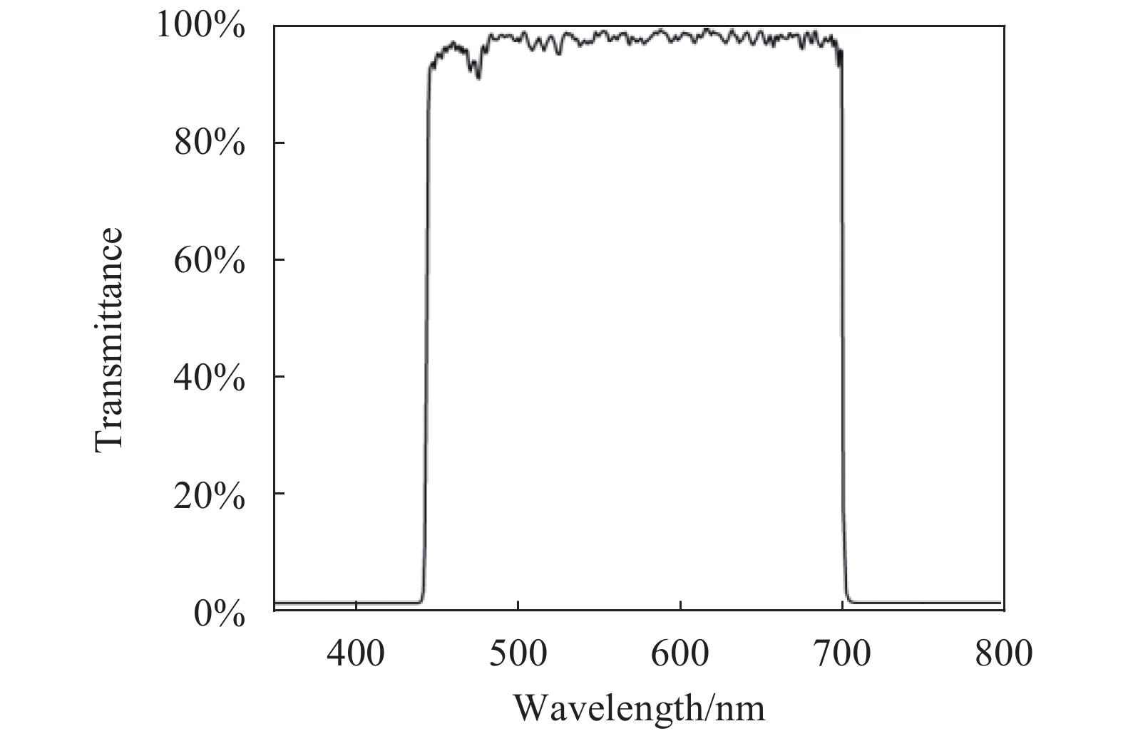
为提高450~700 nm波长处的透过率,需要在背面加镀减反射膜,利用上述方法优化后得到膜系Sub| 0.650 1H 0.592 4L 2.840 9H 2.102 6L |Air。将前、后表面膜系数据导入膜系设计软件中,得到单次曝光多光谱关联成像系统中带通滤波器理论设计曲线如图2所示。

Figure 2. Theoretical design curve of a thin film device in a single-exposure multispectral correlation imaging system
-
该实验是在OZZSQ900真空镀膜机上进行的,该镀膜机配有双“e型”电子枪、考夫曼离子源和双探头晶控系统。将经过清洁处理后的基片放入真空室的工件盘上。当真空度达到4.0×10⁻³ Pa时进行烘烤,待基片温度达180 ℃时维持20 min,开启离子源清洗180 s,当本底真空度达到1.0×10⁻³ Pa开始蒸镀。
薄膜透过率会随着表面散射效应的增大而降低,而表面粗糙度是影响散射效应的主要因素。由膜系设计结果可知,最后一层薄膜为SiO2薄膜,成膜表面粗糙度受沉积速率的影响较大,因此采用控制变量法针对不同的沉积速率进行实验,离子源氧气流量为12 sccm,烘烤温度180 ℃。使用ZYGO白光干涉仪对SiO2薄膜表面形貌进行表征。如图3(a)、3(b)和3(c)分别为0.5 nm/s、0.7 nm/s和0.9 nm/s沉积速率下的SiO2薄膜三维形貌图。

Figure 3. Three-dimensional morphology of SiO2 films with different deposition rates
由图3可以看出,随着沉积速率的增加,薄膜更加均匀致密,但表面缺陷也随之增加,这会影响光束在薄膜表面的散射情况,从而导致薄膜透射损失增大。在不同速率制备的SiO2薄膜表面随机取多点测量,得到薄膜表面粗糙度(Sa、Sq、Sz)平均值如表2所示。
Surface roughness Deposition rates 0.5 nm/s 0.7 nm/s 0.9 nm/s Sa/μm 0.002 2 0.001 2 0.001 7 Sq/μm 0.002 3 0.001 2 0.002 1 Sz/μm 0.059 0 0.026 3 0.136 3 Table 2. Surface roughness of UV-SiO2 film at different deposition rates
评价表面粗糙度的参数随着沉积速率的增加均呈现先减小后增大的趋势,是由于沉积速率越大膜料粒子动能越大,增大了其在基底表面上的迁移率,膜层更加致密,薄膜表面粗糙度减小,但过大的沉积速率又会致使薄膜生长缺陷增加,表面粗糙度变大。当速率为0.7 nm/s时,Sa、Sq、Sz值最小,薄膜表面粗糙度较低,薄膜致密性较好,因此选择SiO2的沉积速率为0.7 nm/s。经实验确定了SiO2和Nb2O5沉积工艺参数如表3所示。
Material Substrate temperature/℃ Degree of vacuum/Pa Deposition rate/(nm·s−1) Flow rate of O2/sccm Kaufman HPE SiO2 180 1.0×10⁻³ 0.7 5 0 Nb2O5 180 1.0×10⁻³ 0.5 35 15 Table 3. Deposition process parameters of Nb2O5 and UV-SiO2
在熔融石英基底上沉积500 nm Nb2O5薄膜,在ZF7基底制备500 nm SiO2薄膜,分别结合Sellmeier和Cauchy色散模型,利用Optichar软件拟合得到材料的光学常数如图4所示。
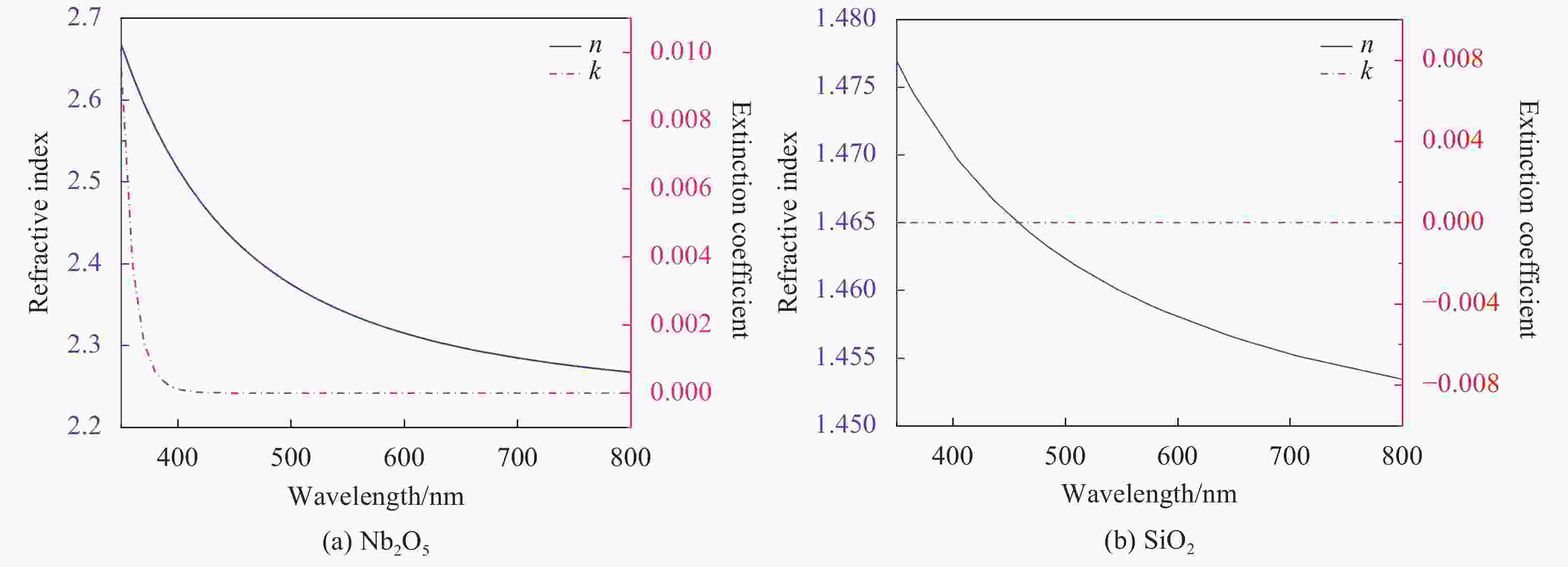
Figure 4. Material optical constants
-
采用美国安捷伦公司生产的Cary5000对带通滤光片进行光谱测试,测试结果如图5所示。
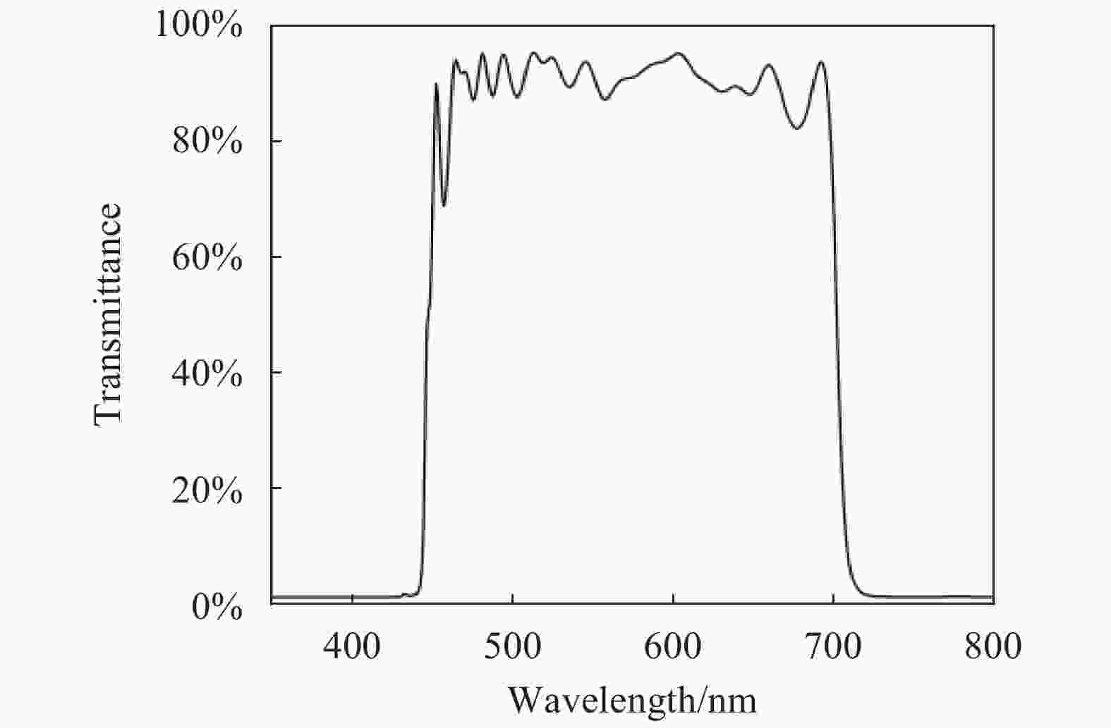
Figure 5. Comparison chart of spectral test curve and design curve
由图5可以看出,测试曲线与设计曲线存在较大的差距,利用TFCalc软件进行逆向反演法分析,薄膜整体厚度均大于设计厚度。实验采用晶控法监控膜层厚度,晶振片谐振频率变化量与薄膜物理厚度增量之间的关系为:
式中:
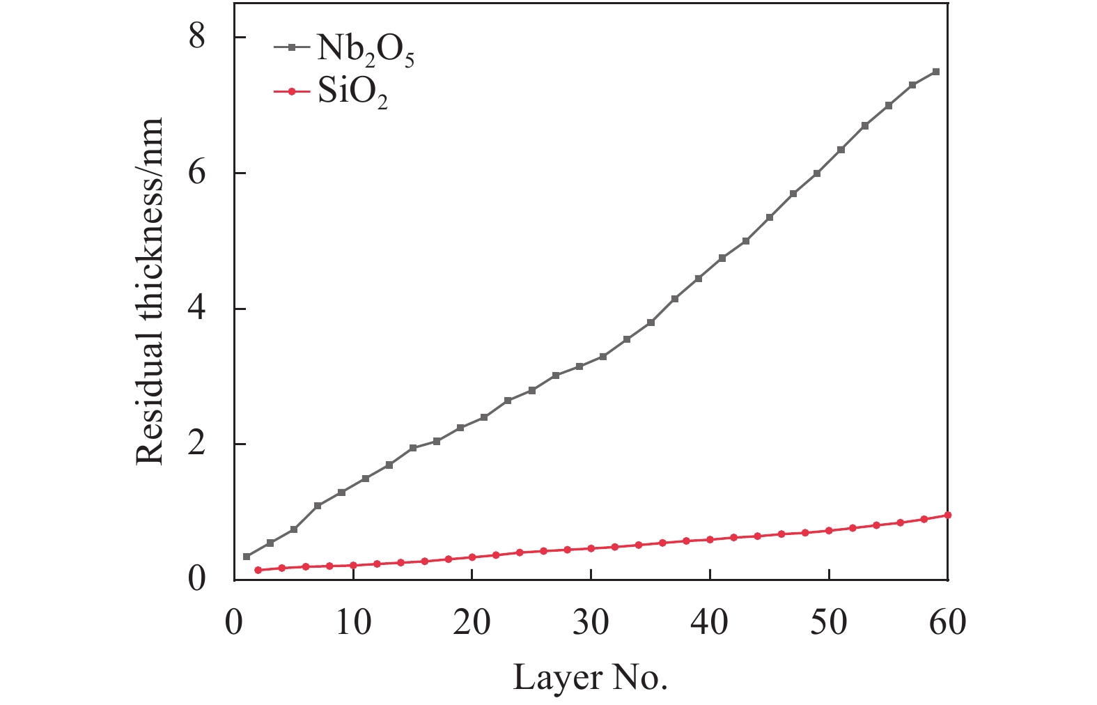
${\rho _m}$ 为薄膜密度;${\rho _z}$ 为石英密度,薄膜材料以及晶振片材料一旦确定,$\dfrac{{{\rho _m}}}{{{\rho _z}}}$ 即为定值;${N_{at}}$ 为常数,其数值大小为1 670 kHz·mm;F为晶振片的谐振基频;$\Delta {d_m}$ 为薄膜厚度增量,是式中唯一变量,由公式(7)可知,随着薄膜厚度的增加,晶振片的谐振频率变化量越来越小,其灵敏度也会随之下降,当下降到一定程度时,振荡器会出现跳频现象,此时的膜厚监控误差会越来越大,误差不断累积从而影响薄膜的光谱特性,也正因为如此,使得残余蒸镀不具备可重复性。残余蒸镀是指蒸镀结束后挡板会自动关闭,但此时真空室内仍存在膜料分子运动,会继续到达基板表面形成薄膜,这一过程中产生的膜厚变化量称为残余蒸镀量。为有效提高膜厚控制精度,对各膜层残余蒸镀进行分析讨论,如图6所示为各膜层残余蒸镀量。
Figure 6. Residual vapor deposition of each film layer
从图中可以看出:Nb2O5薄膜整体的残余蒸镀量过大,因此调整Nb2O5的沉积速率为0.25 nm/s,降低分子运动的动能,减小膜料分子的惯性,从而使残余蒸镀量减小。调整速率后,对材料的光学常数重新拟合计算并应用该光学常数进行膜系设计。同时通过曲线的变化趋势还可以看到,从第35层开始曲线变陡,两种薄膜的曲线斜率均有所增加,Nb2O5的残余蒸镀变化趋势更为明显,说明此时的晶振片灵敏度过低,膜厚监控误差过大,且通过软件分组分析后发现第35~60层膜厚变化量确有异常变化,因此调整监控方法进行实验。当完成第34层蒸镀后,更换监控探头,用另一新晶振片监控后25层。如图7为调整Nb2O5工艺以及监控方法后的各膜层残余蒸镀量。

Figure 7. Comparison of residual evaporation before and after modification
从图中前35层残余蒸镀量的对比可以看出,调整Nb2O5的沉积速率后,其薄膜的整体残余蒸镀量明显降低;同时通过监控方式的修改,有效减小了第35~60层薄膜的残余蒸镀,并与前35层呈现同一规律性变化。由膜系设计结果可知,后25层薄膜的物理厚度普遍低于前35层,因此其残余蒸镀量也相对偏低。
通过实验及以上曲线分析可知,各膜层残余蒸镀量仍不具备可重复性,这是由于其具体数值变化量与膜层厚度有直接关系,因此利用Matlab软件调用ployfit函数来建立膜层厚度与残余蒸镀之间的关系式,进而修正各膜层理论厚度。基于最小二乘法曲线拟合原理,为避免计算量增加引起较大误差,采用多项式二次函数对Nb2O5薄膜理论厚度与残余蒸镀量数据进行拟合,如图8(a)所示为拟合曲线,并得到Nb2O5膜厚
${y_1}$ 与残余蒸镀量${x_1}$ 拟合函数为: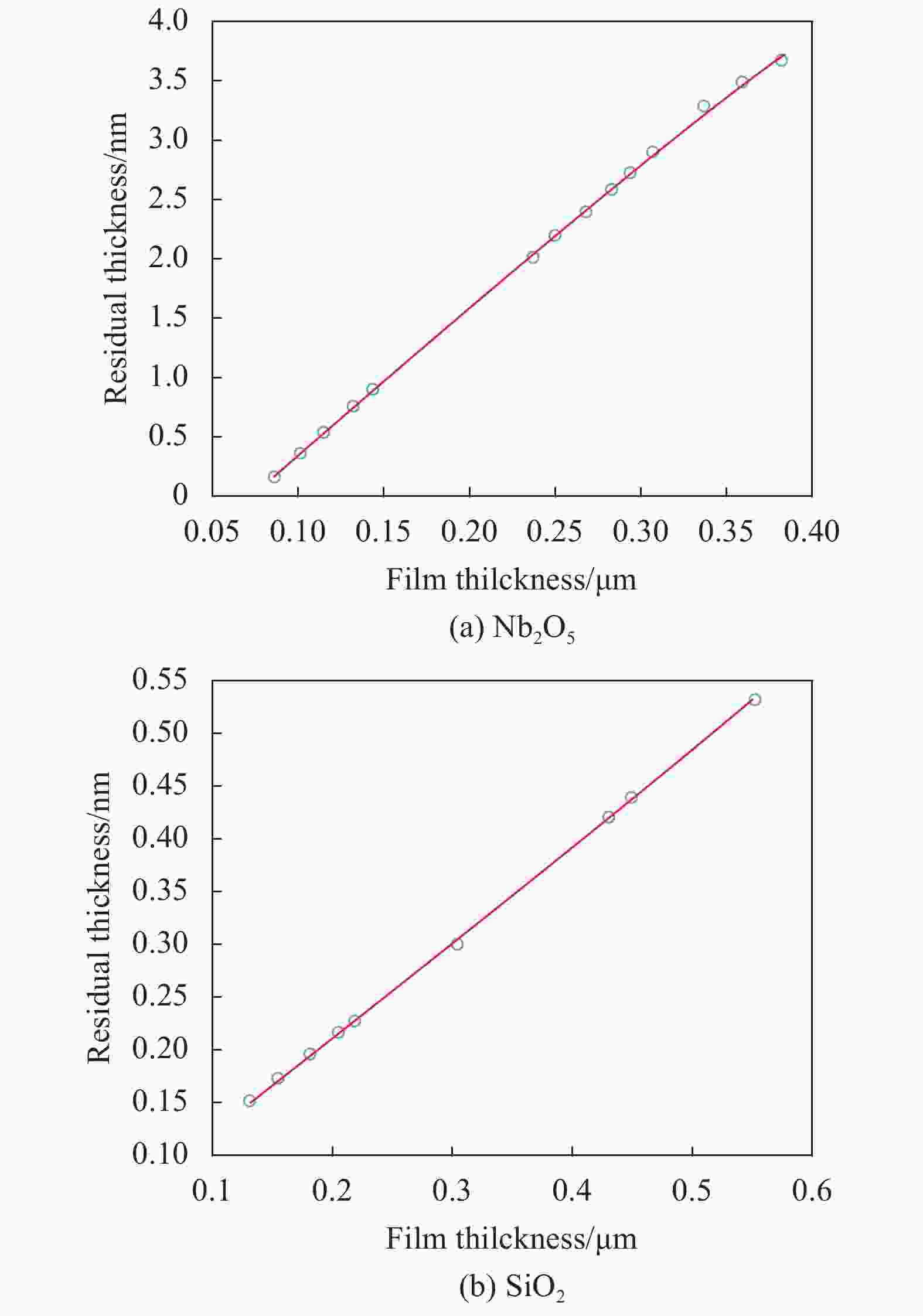
Figure 8. Fitting curve of Nb2O5 and SiO2 film thickness and residual evaporation
同样利用上述方法获得SiO2膜厚与残余蒸镀量数据拟合曲线如图8(b)所示,膜厚
${y_{\rm{2}}}$ 与残余蒸镀量${x_{\rm{2}}}$ 拟合函数为:结合拟合函数修正优化后的膜系,将理论物理厚度代入对应函数计算该厚度下的残余蒸镀量,并在晶控系统内输入每层理论设计厚度与残余蒸镀的差值,再次实验,光谱性能得到明显改善。在背面镀完增透膜后,带通滤波器的光谱曲线如图9所示,在350~440 nm波段,透过率为0.08%,450~700 nm波段平均透过率为98.35%,在710~800 nm范围内透过率为0.02%,满足本课题系统技术指标要求。
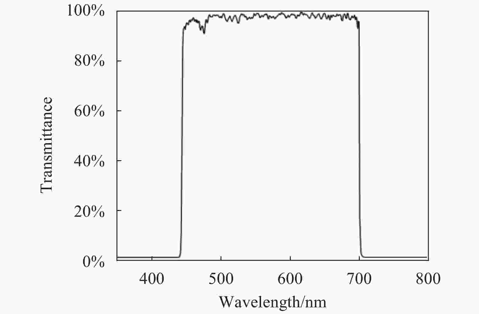
Figure 9. Band pass filter transmittance test curve
-
多光谱关联成像系统常用于地质检测以及成像物理研究等多个领域,因此要求该滤波器具有良好的附着力和耐潮湿性能。按照国家标准GB/T 26331-2010进行测试。
(1) 附着力测试
将剥离强度不小于3 N/cm的胶带紧粘于薄膜表面,确保平整无气泡,并沿垂直薄膜表面方向迅速拉起,重复20次,未出现脱膜现象,附着力良好。
(2) 耐潮湿性测试
将测试片置于温度为50 ℃、相对湿度为95%的环境下24 h,观察测试片表面,未见脱膜现象,耐潮湿性良好。
-
文中根据多光谱关联成像系统的技术要求,对系统所需带通滤波器进行了研制。基于多层膜设计理论,通过目标函数的建立优化膜系结构,完成了带通滤光膜的设计,并使用电子束蒸发法进行研制。通过分析SiO2沉积速率对薄膜表面粗糙度的影响,优化SiO2膜沉积速率,使薄膜表面缺陷得到了改善,降低了表面散射。通过对各膜层残余蒸镀的分析讨论,调整监控方式,减小了薄膜的残余蒸镀量;利用最小二乘法原理建立了膜层厚度与残余蒸镀量之间的拟合函数,提高了制备过程中膜厚控制精度,最终获得450~700 nm波段平均透过率为98.35%的带通滤波器,通过了环境测试,满足系统使用要求。
Research on the bandpass filter used for single-exposure multi-spectral ghost imaging system
doi: 10.3788/IRLA20200169
- Received Date: 2020-06-07
- Rev Recd Date: 2020-07-15
- Available Online: 2020-09-22
- Publish Date: 2020-09-22
-
Key words:
- multi-spectral /
- ghost imaging /
- single-exposure /
- bandpass filter
Abstract: Different from the traditional point-to-point imaging, multi-spectral ghost imaging retrieve the image information of the target by means of modulation and demodulation. In this paper, a single-exposure multi-spectral ghost imaging system based on a fixed phase modulator was built, and the development of thin-film devices in the system was completed. In the thin film, BK7 glass was chosen as the substrate, niobium oxide (Nb2O5) and silicon dioxide (SiO2) were used as the high and low refractive index materials, respectively. Based on the basic theory of optical thin film, the simulation analysis and the film system design were carried out by the film system design software, through setting up evaluation function for film optimization, the design of 450-700 nm band-pass film filter with an incidence angle of 0°-30° was realized and the research and development of this film was completed on OZZSQ900 box-type vacuum coating machine. Through optimizing deposition rate of SiO2 film, the surface defects and scattering loss of film were reduced. The residual evaporation deposition of film was analyzed, the fitting function between film thickness and residual evaporation deposition by least square method was established, monitoring ways was adjusted, residual evaporation deposition was reduced and the accuracy of film thickness control during preparation process was improved. From the test performed by Agilent Cary5000 spectrophotometer, the transmittance is less than 0.5% in the bands of 350-440 nm and 710-800 nm, and higher than 98% in the range of 450-700 nm at the incident angle of 0°-30°, which meets the requirements of the imaging system. The study has important practical significance and engineering value.


 DownLoad: