


-
多余物是指产品技术状态规定以外的一切物质[1-2],包括可动与不可动多余物。探测器杜瓦组件内的不可动多余物在器件冲击或振动过程中也会变成可动多余物。这些多余物进入器件光路,即杜瓦冷屏结构中时,有可能会产生衍射效应,进而影响到焦平面局部光场分布,导致图像上出现“黑斑”或“泊松亮斑”[3]。这些异常斑会严重影响红外探测器对目标信息的提取和分析,降低探测器识别能力[3-5]。因此,研究探测器杜瓦组件内多余物的光学衍射现象,并控制多余物出现显得十分必要,目前国内关于此方面的研究报道还比较少。其实除上述图像异常外,多余物还会导致其他产品失效问题,比如产生信号串扰、较大尺寸的颗粒跨接器件中不连续的导电部分使电路短路[1]等。为了尽可能避免多余物所造成的各种危害,文中不仅对常用探测器杜瓦封装组件内多余物颗粒的衍射规律进行了分析,同时也探讨了杜瓦封装过程中多余物的控制措施。
-
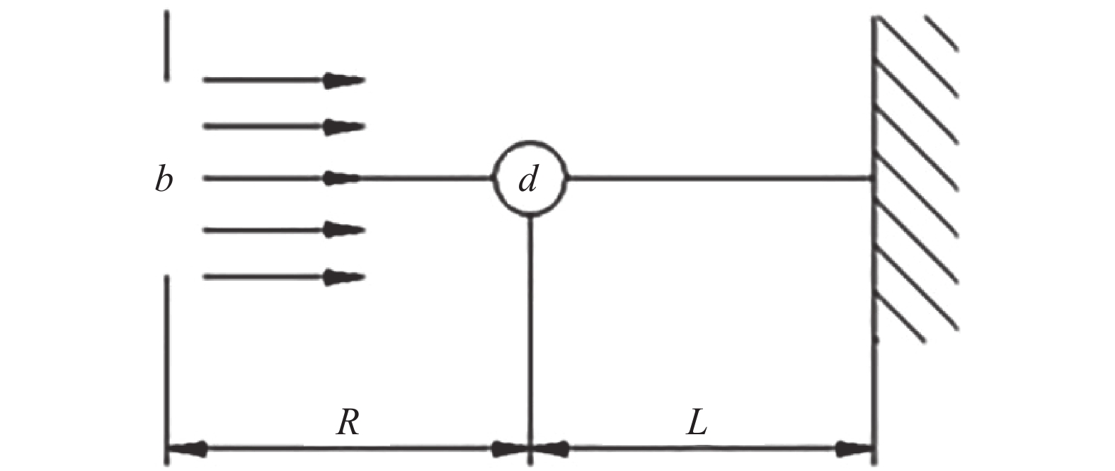
在杜瓦组件中多余物主要是一些机械加工碎屑、毛刺、焊渣以及涂层脱落物等,为了简化分析,假设多余物为直径d的球形颗粒。图1展示了球形多余物颗粒在探测器组件光路中与焦平面以及冷屏的位置关系。

Figure 1. Optical path sketch
在图1中,入射光为平行光,入射波长为λ(单位: μm),b为冷屏开口(单位:mm),d为多余物颗粒直径(单位:mm),R是多余物到冷屏开口的距离(单位:mm),L为多余物与光敏面的距离(单位:mm),冷屏高H=L+R。根据菲涅尔衍射理论,光束经过多余物呈现衍射斑需要满足光束到达多余物时的光斑半径
$\Delta x$ 大于多余物颗粒的直径d[6]。由于光束通过冷屏圆形开口后形成的艾里光斑的半发散角$\Delta \theta $ 为[7-8]:则对应到达多余物时艾里光斑的半径
$\Delta x$ 为:当
$\Delta x$ 大于多余物颗粒直径时,无法挡住光斑的大部分光强,多余物便可以得到充分照明,从而能再次通过多余物颗粒产生衍射效应,使得焦平面上呈现衍射斑。衍射斑可分为两种,多余物颗粒呈圆形时,颗粒边缘的衍射光到达颗粒正下方对应圆心位置处的相位相同,可得到中心有亮斑的黑斑,即“泊松亮斑”。若多余物颗粒边缘不光滑,形状偏离圆形,那么颗粒边缘衍射的光到达颗粒下方投影中心的相位不同,也就无法得到中心亮斑(或中心亮斑非常弱),此时呈现出中心没有亮斑的黑斑[7-10]。
故结合理论分析,光束通过冷屏开口后,经直径为d的多余物颗粒在焦平面上形成衍射斑的条件为:
而根据菲涅尔衍射理论,同样也可估算出其对应在焦平面上形成的衍射斑直径D为[6-7]:
要产生明显的衍射现象,D值当小于焦平面的对角线长度C(单位:mm)[3-4],即:
其中公式(3)右侧项计算值为颗粒满足衍射条件的最大直径dmax,多余物颗粒直径d比dmax小时会产生衍射效应。因此,当波长λ、冷屏开口b及多余物位置R不变时,多余物越小就越容易形成衍射斑;而其他因素不变,冷屏开口b越大,dmax越小,符合公式(3)能产生衍射的d值区间也就越小,则越难形成衍射斑;同理,入射波长λ越长,多余物产生衍射越容易。结合公式(3)和公式(5)可以估算出探测器杜瓦内多余物颗粒可发生明显衍射现象的尺寸范围。
由于在杜瓦冷屏设计中,冷屏高度H和冷屏开口b尺寸需满足红外光学系统F数限制,同时兼顾杜瓦结构的安装尺寸,所以产品设计中往往针对不同的冷屏高度H会匹配相应的冷屏开口尺寸b,即H与b相联系。不同的杜瓦结构H和b不同,典型的几种红外探测器冷屏,其H和b取值分别为20 mm和25 mm、30 mm和10 mm、12 mm和18 mm。文中针对这几种杜瓦冷屏的光路,进行了多余物衍射尺寸的计算,其中入射波长均取10 μm,具体如图2所示。
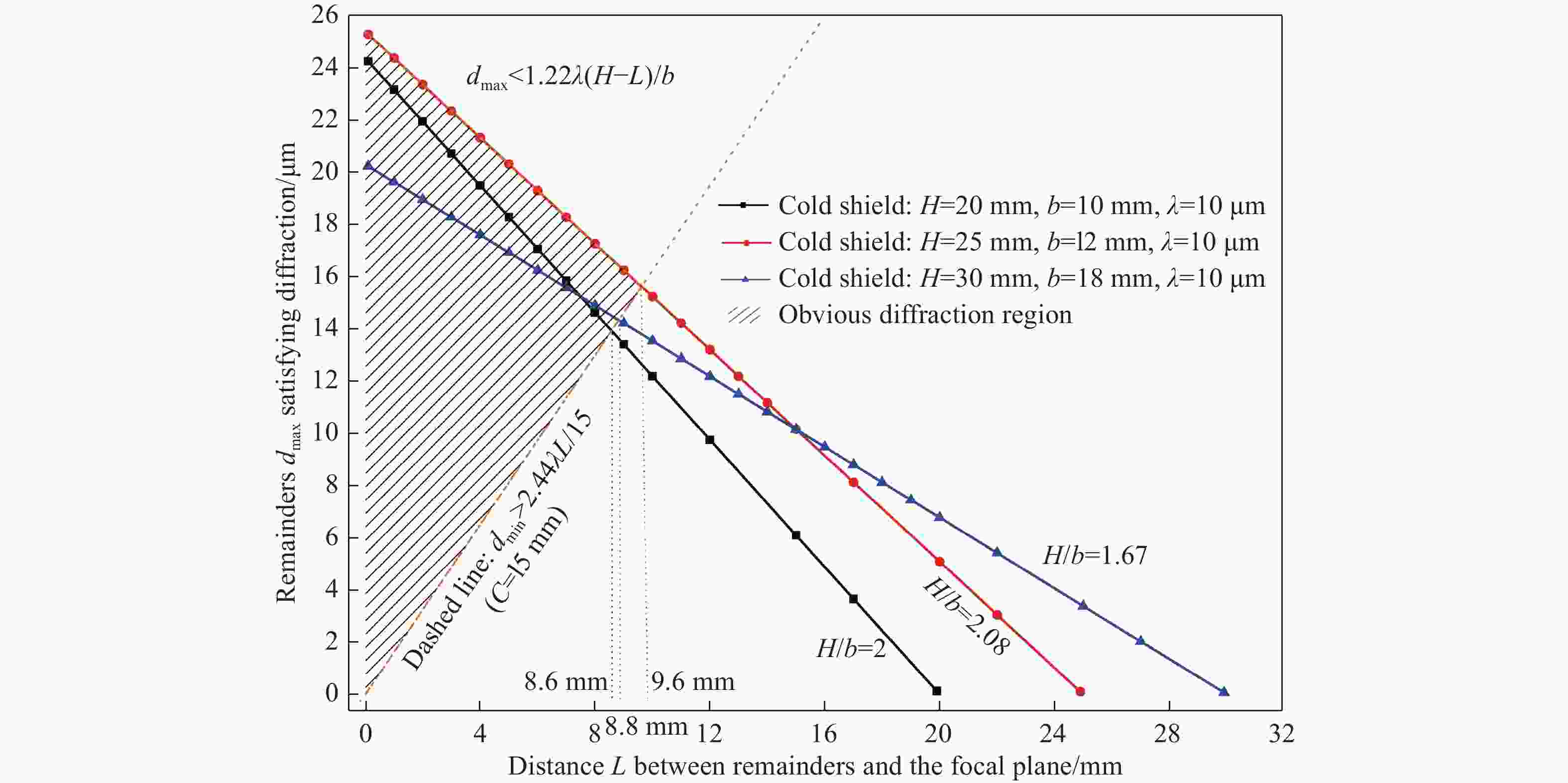
Figure 2. Distance L between remainders and the focal plane-remainders diameter dmax satisfying diffraction curves for different Dewar cold-shielding structures, slant dashed line 2.44λL/C denotes diameter lower limit value for diffraction, shadow region indicates obvious diffraction. Focal plane diagonal length C=15 mm
图2中的实曲线展示了形成衍射斑所要求的最大多余物尺寸dmax随其距离焦平面距离L的变化情况。颗粒离焦平面越近,L越小,dmax就越大。不同的实曲线分别代表不同冷屏结构下的dmax计算结果,结果表明L较小时,冷屏高度H与开口b的比值越大,各位置处对应的dmax越大,即多余物可产生衍射的d值区间越大,越容易发生衍射现象。
由于要产生明显的衍射斑,需要衍射斑直径Dmax=(2.44λL/dmin)<C,此处C为常见的探测器焦平面对角线长15 mm,将C=15 mm代入公式(5)的右侧,可在图2中画出dmin=2.44λL/15的斜虚线,此虚线上方满足公式(5),能产生明显的衍射斑。结合公式(3),实曲线dmax以下的颗粒直径才能满足发生衍射的条件,这样,由斜虚线与实曲线所交成的阴影区域,即为能发生明显衍射现象的多余物颗粒尺寸范围。斜虚线2.44λL/C与实曲线1.22λ(H-L)/b的交点(LC, dc)处LC值为:
如图2所示,C取15 mm,三种冷屏结构中最大的LC值为9.6 mm,对应H/b值最高的结构,也是明显衍射区(图2阴影区)范围最大的结构。
综上所述,为了减少衍射斑的出现,应设计H/b较小的冷屏结构,多余物筛查时更应当注意距离焦平面较近的位置,即L<LC的区域。比如针对这几种杜瓦而言,应分别重点筛查L<8.6 mm、L<8.8 mm、L<9.6 mm的区域(图2),并且在对应的0<L<Lc区间内,需要尽量控制直径位于图2所示阴影区域内的颗粒出现。
-
由第1节的分析可知,一定尺寸范围的多余物颗粒容易产生光学衍射现象,从而引起探测器成像异常;但多余物的危害不仅于此,较大尺寸的多余物会造成划伤或跨接导电部分致使电路失效;而较小尺寸的颗粒位于间距较小的互连线间时也容易引起信号串扰[1-2]等问题。因此,为了提高探测器组件的可靠性,应通过各种检测手段及时去除多余物,并分析其来源,以便控制组件内多余物的数量及大小。
检测多余物的主要方法包括显微镜镜检、非破坏性X射线检测法以及粒子碰撞噪声检测(PIND)。对于较大颗粒物的有无可以通过摇晃听声音或者显微镜镜检来确定,而对于较小的颗粒,可以通过X射线成像法检测,根据X射线图像,能判断多余物的外形、位置和大小。此外晃动器件后,再进行拍摄,对比两次X射线照片中多余物的位置,还可以验证多余物是否可动。X射线的分辨率一般为0.025 mm,当多余物颗粒更小或者更难检测时,可以借助PIND法,通过分析多余物振动时的声音信号,以判别多余物的有无及类别,目前在PIND中结合人工神经网络来识别微粒,能达到98%的识别准确率[2]。PIND较适合于判别微小的硬质松动颗粒。
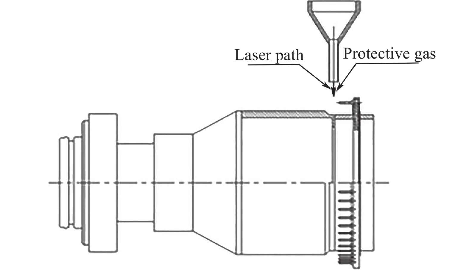
探测器杜瓦组件中的多余物主要来源于机械加工过程、焊接装配过程、表面处理过程、吸气剂安装以及粘片过程等。在机械加工过程中由于各种工艺限制很容易留下尖角、金属残渣及陶瓷粉末等多余物。另外,杜瓦主体装配多采用激光焊接工艺,焊接过程当中不可避免地会产生粉尘及金属飞溅,为防止杜瓦零部件在焊接过程中氧化又必须加以吹气保护,如图3所示,激光光路及保护气体气路都从激光焊接机喷嘴部位出来,导致保护气体将金属粉尘四处吹散,而杜瓦右端陶瓷引线环处有较大开口,使得粉尘有进入到杜瓦腔体内部的可能性,若处理不干净则会残留于杜瓦内部,当探测器振动成像时粉尘就会随之跳动导致黑斑等衍射斑的出现。

Figure 3. Dewar precision assembly sketch
其次,冷屏作为探测器组件光路中的重要零件,其黑化工艺也是引入多余物颗粒不可忽视的环节,冷屏黑化层固化后涂层较硬且脆,若冷屏黑化之前局部表面未处理干净,导致涂层与基体结合不牢;加之黑化涂层内部的残余应力,在受到高低温或者机械冲击时会导致涂层破裂,进而带入多余物到光路中形成衍射现象。同样,吸气剂也是硬脆物质,在其安装或振动过程中,也容易发生破损或脱落而带来多余物颗粒[11]。最后,封装过程中使用棉织材料及滤纸会产生纤维等多余物,如下图4所示,这些细小多余物很容易因静电吸附在芯片表面并残留下来,造成成像时出现成像异常的图像。
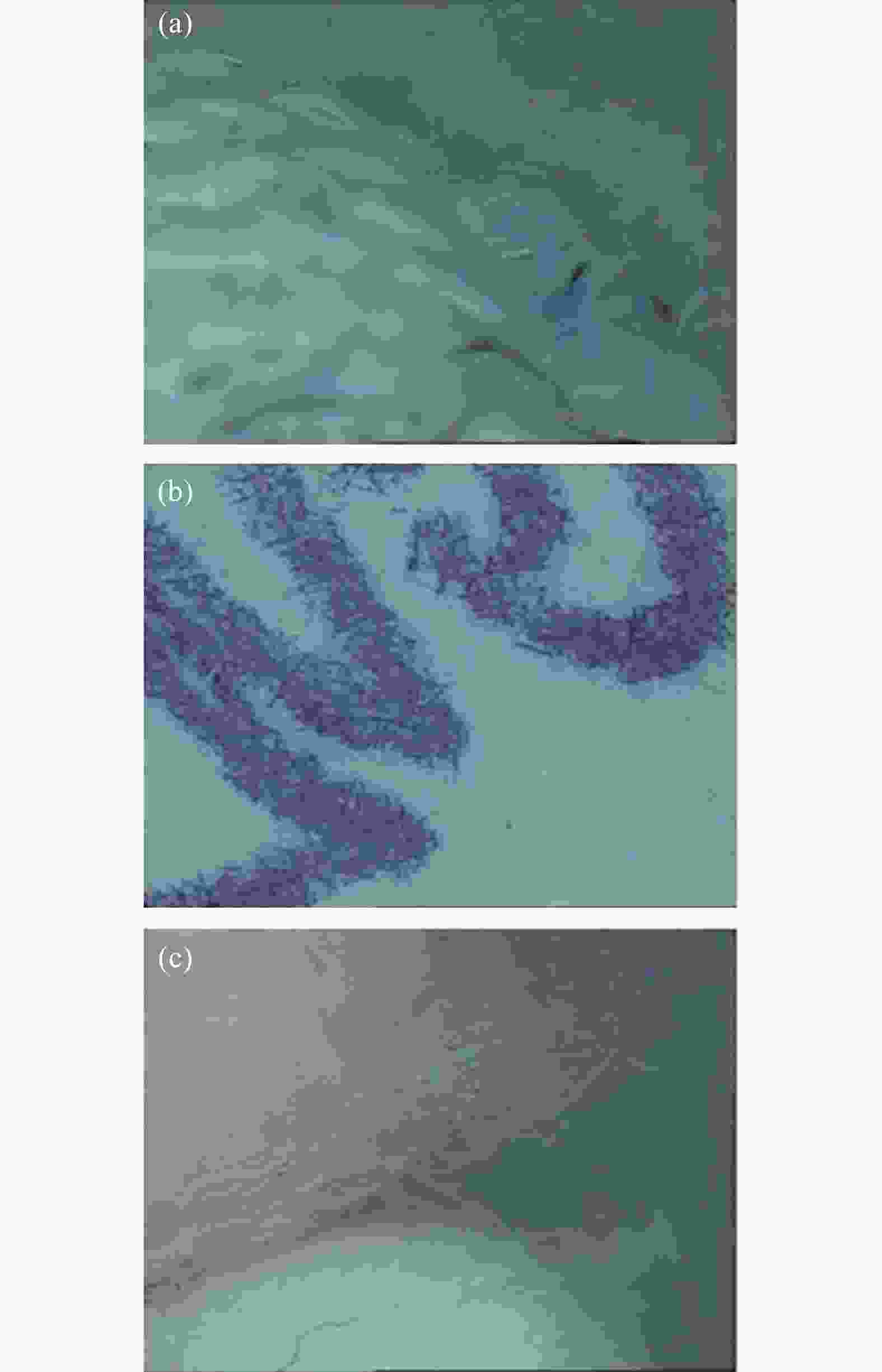
Figure 4. Fiber remainders. (a) Antistatic gloves fiber; (b) Filter paper fiber; (c) Cotton swab fiber
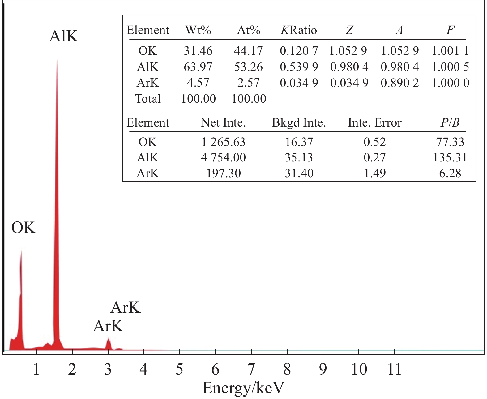
通过多年的生产实践,在探测器杜瓦组件中观察到的多余物多为:金属毛刺、陶瓷颗粒、焊接熔渣、锈蚀、棉纤维、吸气剂掉粉、黑化层脱落物、陶瓷基板介质层碎裂物、芯片边缘颗粒、划片硅渣、引线键合起球或失败焊点等。无机多余物的成分分析可以借助SEM能谱分析来判断。图5中便展示了一只杜瓦组件中残留多余物的能谱图,由图5可知,多余物成分为氧化铝陶瓷,其来源有可能为封装用装载基板。

Figure 5. Energy spectrum analysis of remainders in an infrared detector
多余物来源与产品设计、工艺及材料制备密切相关。为了减少多余物对探测器带来的危害,结合理论分析与生产经验,目前可采取以下适当措施来控制多余物:
(1)结合第1节的分析计算,将低温滤光片放置在冷屏内Lc对应位置,使滤光片、冷屏与焦平面芯片间形成相对封闭的腔体,防止外部多余物进入;该腔体为多余物形成衍射斑的敏感区域,应重点控制其内部的洁净度。
(2)杜瓦结构设计上尽量减少细小台阶和锐边设计,以免出现机加毛刺或划伤化学表面而产生多余物;此外设计时应尽量提出清角以及表面光洁度等要求;金属零件应多选用不易腐蚀氧化的材料;吸气剂材质则宜采用不易掉粉的型号,同时进一步改进吸气剂安装设计,避免刮擦导致吸气剂颗粒脱落。
(3)在焊接过程中可对焊缝外的区域进行保护,减少飞溅;优化焊接能量以减少熔渣;另外,还应改善黑化涂层粘接等工艺,规范粘接操作,提高黑化涂层的牢固度;
(4)确保工作环境的洁净度,100000级以上;加严产品各生产环节中的多余物检验及清理工作。
(5)对检查出的多余物结合成分分析手段,以便知其来源加以防范,对产生过的多余物种类以及来源都应记录在案,以便后续改进工艺来控制多余物。
图6(a)是未进行多余物控制前,红外探测器振动过程中的焦平面图像,其中有明显的异常“黑斑”出现,采取多余物检测以及控制措施后,探测器像面上出现黑斑现象的概率大大降低,像面正常的红外探测器振动图像如图6(b)所示。

Figure 6. Images of infrared detector during vibration. (a) Image with black spot; (b) Normal image
-
一定尺寸大小的多余物颗粒在探测器光路中会产生光学衍射,使像面上呈现衍射斑。根据菲涅尔衍射理论进行计算,结果表明距离焦平面不同位置处的多余物颗粒,其产生明显衍射现象所要求的尺寸范围不同,一般波长越长、颗粒距离焦平面越近就越容易出现衍射现象。对于不同的探测器杜瓦组件,容易产生衍射的位置为距离焦平面距离L<LC的区域。为了避免像面上出现衍射斑同时减少多余物对探测器的其他危害,可以通过改进杜瓦结构的设计和生产工艺,实现对多余物的控制。
Diffraction analysis and control of remainders in infrared detector Dewar packaging
doi: 10.3788/IRLA20200177
- Received Date: 2020-05-15
- Rev Recd Date: 2021-01-10
- Available Online: 2021-05-12
- Publish Date: 2021-03-15
-
Key words:
- infrared detector /
- Dewar /
- remainders control /
- diffraction /
- black spot
Abstract: Remainders with a certain size in the infrared detector assembly easily cause the diffraction phenomenon in the optical path of infrared detector in service, which would change the local luminous flux distribution on the focal plane, resulting in 'black spot' and 'Poisson bright spot ' on the image. In order to reduce the occurrence of such abnormal images, according to Fresnel diffraction theory, the remainder particles diameter satisfying the diffraction spot formation for several typical detector Dewar assemblies was calculated, and the relationship among the remainders dimension, Dewar structure, wavelength and diffraction spot was also analyzed. The results show that diffraction is more likely to happen for longer wavelength and smaller distance between remainders and focal plane; for different detector Dewar assembly, the position inclined to diffraction is the region where the distance denoted by "L" between remainders and focal plane satisfies the equation "L<LC". Besides, combined with the production practice, some corresponding measures to control the remainders were offered. These conclusions in the article provide a reference for the infrared detector production design and engineering application.


 DownLoad: