


-
Thermophotovoltaic (TPV) cells generate electricity by converting the photons emitted from the high-temperature emitter that can be heated by a wide range of energy sources including industrial waste heat[1], solar energy[2], and micro radioisotopes[3]. Up to now, TPV cells have been realized using various III-V semiconductor materials with low bandgap energies (Eg) corresponding to these emitter wavelength range. These materials such as InGaAs grown on InP substrates[4] and GaSb/InGaAsSb grown on GaSb substrates[5-6] have aroused great interest of researchers. GaSb cells are ideal converters for combustion-based thermophotovoltaic systems, which have been widely used in various types of TPV systems [7-9]. It is well known that the bandgap of GaSb material is 0.72 eV which is suitable for the low temperature heat sources of interest.
In the past, Zn diffusion into n-type GaSb bulk substrates has been the most common technology to manufacture GaSb TPV cells. However, recently researchers have paid more and more attention to the epitaxial growth of n-type and p-type GaSb layers, mainly using the MOCVD technique and MBE technique [9].
In this paper, we restrict ourselves to the low-bandgap material of GaSb. Other important low-bandgap semiconductors such as InGaAsSb or InGaAs/InP for TPV application are not considered. In this work, large area GaSb TPV cells with 1 cm×1 cm device area were fabricated using MBE. And the TPV cells have different electrode shape, one is a simple electrode, the other is a grating electrode. By comparing the differences between the two, we can find that the GaSb TPV cells with the grating electrode have better device performance in short circuit current density and fill factor.
-
High quality of epitaxial layers of the devices is necessary for good performance of TPV. The GaSb material in this paper was grown by molecular beam epitaxy (MBE) system using a GaSb substrate. The MBE system is the Veeco GEN II solid-source MBE system and the GaSb substrate is the heavily Te-doped GaSb (001) substrate. Samples are controlled by high resolution X-ray diffraction (HR-XRD) and Atomic Force Microscopy(AFM) for quality management.
The proposed TPV cells just contain the GaSb layers grown on the GaSb substrate. Therefore we only need to find the optimal growth condition for the GaSb epilayers grown on the GaSb substrate. The experiment started with adjusting the growth condition such as growth temperature and V-III ratio. Finally, we found the most suitable growth condition and obtained the high-quality epilayers of the GaSb TPV cells. In the experiments, the GaSb substrate was deoxidized first at temperature above 600 ℃. Then we had to observe the reconstruction temperature of the GaSb substrate which is important to set the growth temperature. The TPV epilayers were grown at temperature of 110 ℃ above the reconstruction temperature. And after many comparative experiments, we found that the most appropriate V-III ratio is 12.
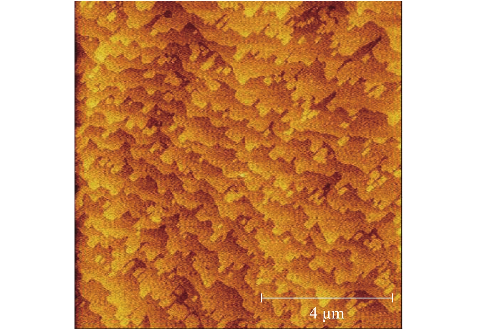
We identify the quality of the GaSb TPV cells by means of the HR-XRD and the AFM. The HR-XRD pattern of the epilayers was shown in Fig.1. An excellent crystalline material quality with a relative lattice mismatch<0.5‰ was measured which is shown in Fig.1. Good surface morphology of the epilayers was observed by AFM image which is shown in Fig.2. The root mean square (RMS) of surface morphology is only 1.5 Å (1 Å=0.1 nm) over a 10 μm×10 μm area, and the atomic steps are clear in the image. In conclusion, the quality of the epilayers of the GaSb TPV cells is great.

Figure 1. High-resolution XRD pattern of the epilayers
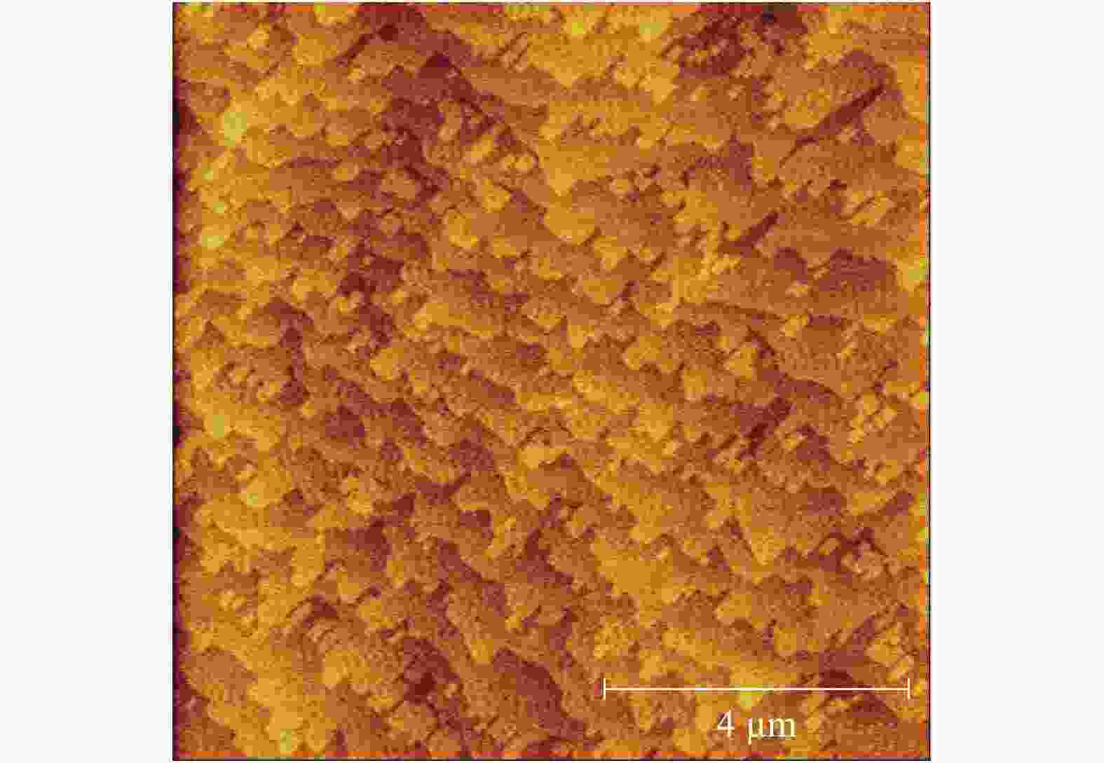
Figure 2. AFM image of the epilayers of the TPV devices
-
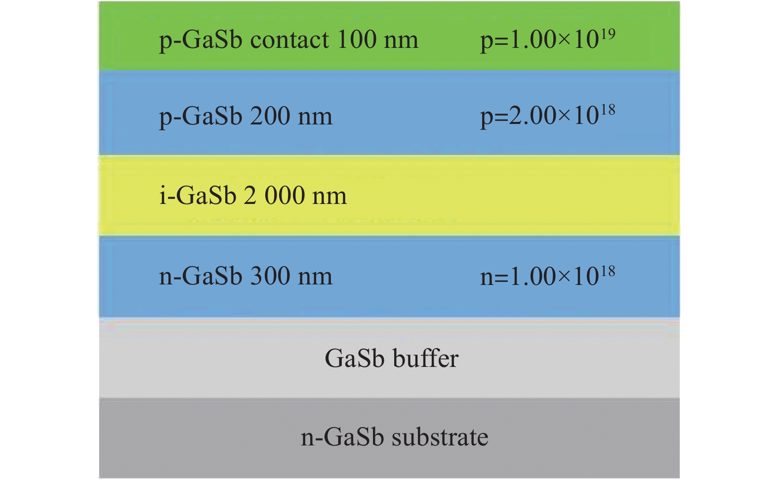
TPV systems generate electricity by converting the photons emitted from the high-temperature emitter. Therefore, the GaSb TPV cells must absorb as much photons as possible. We design the GaSb TPV structure according to the absorption coefficient of GaSb versus wavelength at 300 K[10-11]. The absorption area of the GaSb TPV cells must have enough thickness to satisfy the absorption coefficient of photons.
Figure 3 shows the schematic cross-section of the GaSb TPV structure. The epitaxial structure was grown on an n-type GaSb substrate by using the MBE method. From the top to the bottom, these layers are sequentially named as contact layer, p-GaSb layer, i-GaSb layer, n-GaSb layer, GaSb buffer layer, GaSb substrate. The contact layer and the p-GaSb layer are doped with Be as the p-type. The Be impurities are well behaved acceptors with high hole concentrations, which is helpful to improve the performance of the absorption and external quantum efficiencies[12-13]. The doping level of the contact layer is 1×1019 cm−3 and the doping level of the p-GaSb layer is 2×1018 cm−3. The n-GaSb layer is doped with Te as the n-type at doping levels of 1×1018 cm−3. The Te doping is suitable for n-type GaSb doping at doping level of 1×1018 cm−3[14]. According to the absorption coefficient of GaSb versus wavelength at 300 K[10-11], the absorption coefficient of GaSb is above 104 cm−1 in the near infrared band. In our GaSb TPV structure, the thickness of the i-GaSb layer is 2000 nm, which can ensure the light absorbtivity to reach 90%.

Figure 3. Structure of the GaSb TPV
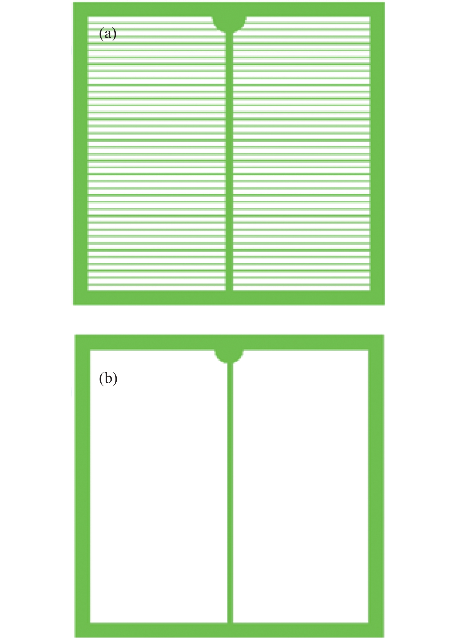
In this work, two kinds of GaSb TPV cells with 1 cm×1 cm dimensions that have different electrode shape were fabricated. The structure of two GaSb TPV cells is shown in the Fig.4. The GaSb TPV cell shown in the Fig.4(a) has a grating electrode and the GaSb TPV cell shown in the Fig.4(b) has a simple electrode. The two kinds of GaSb TPV cells have a same epitaxial structure but have different electrode shapes. Compared with the simple electrode, the grating electrode has a row of 10 μmwide electrodes. The distance between the grating electrodes is 0.25 mm.

Figure 4. Electrode shapes of different GaSb TPV cells. (a) A grating electrode; (b) A simple electrode
By comparing the differences between the two, we can study the influence of electrode structure on device performance. The GaSb TPV cells adopts front electrode and back electrode which are deposited by the electron beam evaporation. The front electrode is deposited using Ti (50 nm)/Pt (50 nm)/Au (100 nm) and the back electrode is deposited using AuGeNi (50 nm)/Au (300 nm). Finally, through the flip-chip bonding, the GaSb TPV devices are brought in contact with the readout circuit.
-
This section discusses the results of the electro-optical characterization of the GaSb TPV cells. Devices will be evaluated regarding the dark current density, open circuit voltage, short circuit current density, photoelectric conversion efficiency and fill factor.
In order to characterize the current characteristics of the TPV cells, I-V measurements have been performed in the dark environment. The Fig.5 shows a typical I-V curve for a large-area 1 cm×1 cm epitaxial GaSb TPV under dark conditions. As shown in the Fig.5, The I1 shows the dark current of the TPV cell with a grating electrode and the I2 shows the dark current of the TPV cell with a simple electrode. At the same forward voltage, the dark current of the TPV cell with a grating electrode is general 50% higher than that of the TPV cell with a simple electrode. The dark current of the TPV cells shows that the grating electrode has higher collection efficiency for carriers and lower resistance.

Figure 5. Dark I-V curve of the GaSb TPV cells 1 cm×1 cm dimensions
In order to obtain the photovoltaic characteristics of the GaSb TPV cells, we have measured the I-V curves under solar simulation and infrared light. From the I-V curves of the GaSb TPV cells, we can calculate the performance parameter such as the open-circuit voltage, the short-circuit current density, the fill factor and the photoelectric conversion efficiency under solar simulation and infrared light.
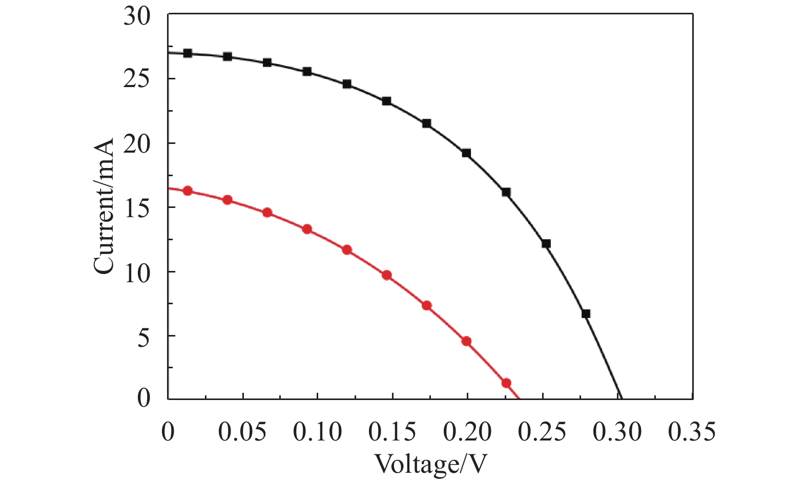
Figure 6 shows the I-V curves of the GaSb TPV cells under solar simulation. The black curve shows the I-V curve of the TPV cell with a grating electrode and the red curve shows I-V curve of the TPV cell with a simple electrode. By comp
aring the I-V curves of the two kinds of GaSb TPV cells, we can see that the TPV cell with a grating electrode has a great improvement in short-circuit current density and the fill factor. Under one-sun illumination, the TPV cell with a grating electrode exhibits an open-circuit voltage of 0.303 V and a short-circuit current density of 27.1 mA/cm2. And the TPV cell with a simple electrode exhibits an open-circuit voltage of 0.235 V and a short-circuit current density of 16.6 mA/cm2. 
Figure 6. I-V curve of the GaSb TPV cells under solar simulation
From the I-V curves of the GaSb TPV cells, we can calculate the P-V curves. The P-V curves are shown in the Fig.7. The black curve shows the P-V curve of the TPV cell with a grating electrode and the red curve shows P-V curve of the TPV cell with a simple electrode. It can been seen that the output power of the TPV cell with a grating electrode is much higher than that of the TPV cell with a simple electrode under one-sun illumination. Therefore, the photoelectric conversion efficiency of the TPV cell with a grating electrode is much higher than that of the TPV cell with a simple electrode.

Figure 7. P-V curve of the GaSb TPV cells under solar simulation
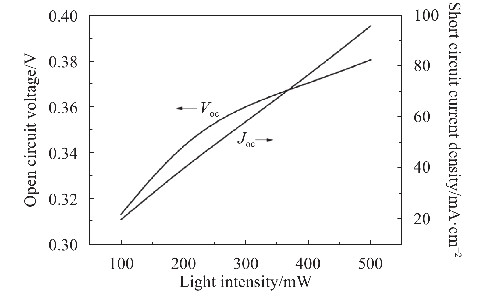
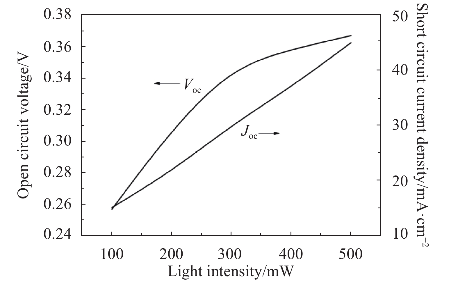
The performance of the GaSb TPV cells under different incident infrared light intensities is shown in Fig.8 and Fig.9 where the change rule of the open-circuit voltage and the short-circuit current density with incident infrared light intensity is given. The incident infrared light is emitted from the 1 μm infrared light source. In theory, the GaSb material has high absorption coefficient for 1 μm infrared photon[10-11]. The Fig.8 shows the performance of the TPV cell with a grating electrode and the Fig.9 shows the performance of the TPV cell with a simple electrode. And the Fig.10 shows the comparisons of the short-circuit current density versus the open-circuit voltage for the TPV cells.
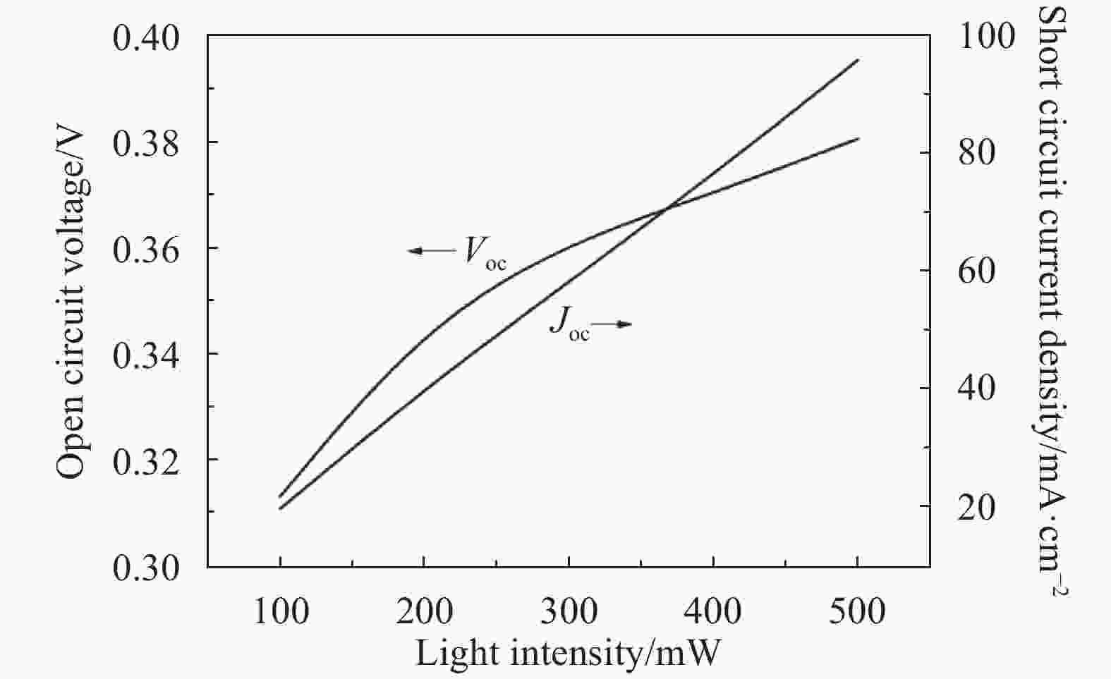
Figure 8. Open-circuit voltage and the short-circuit current density of the TPV cell with a grating electrode
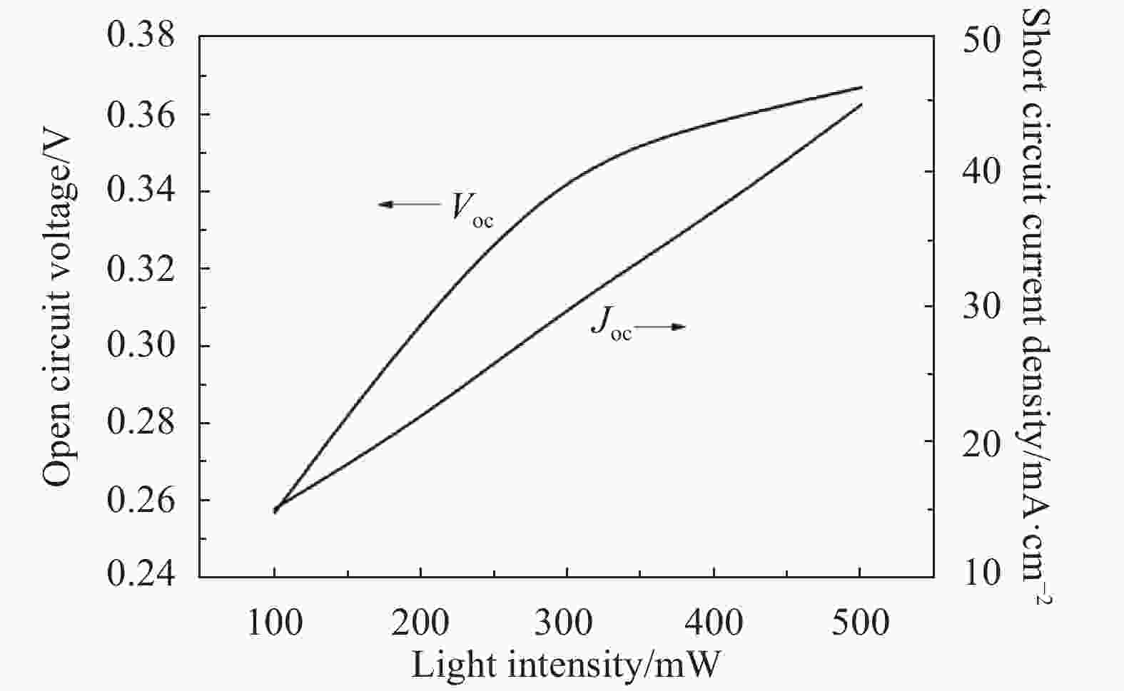
Figure 9. Open-circuit voltage and the short-circuit current density of the TPV cell with a simple electrode
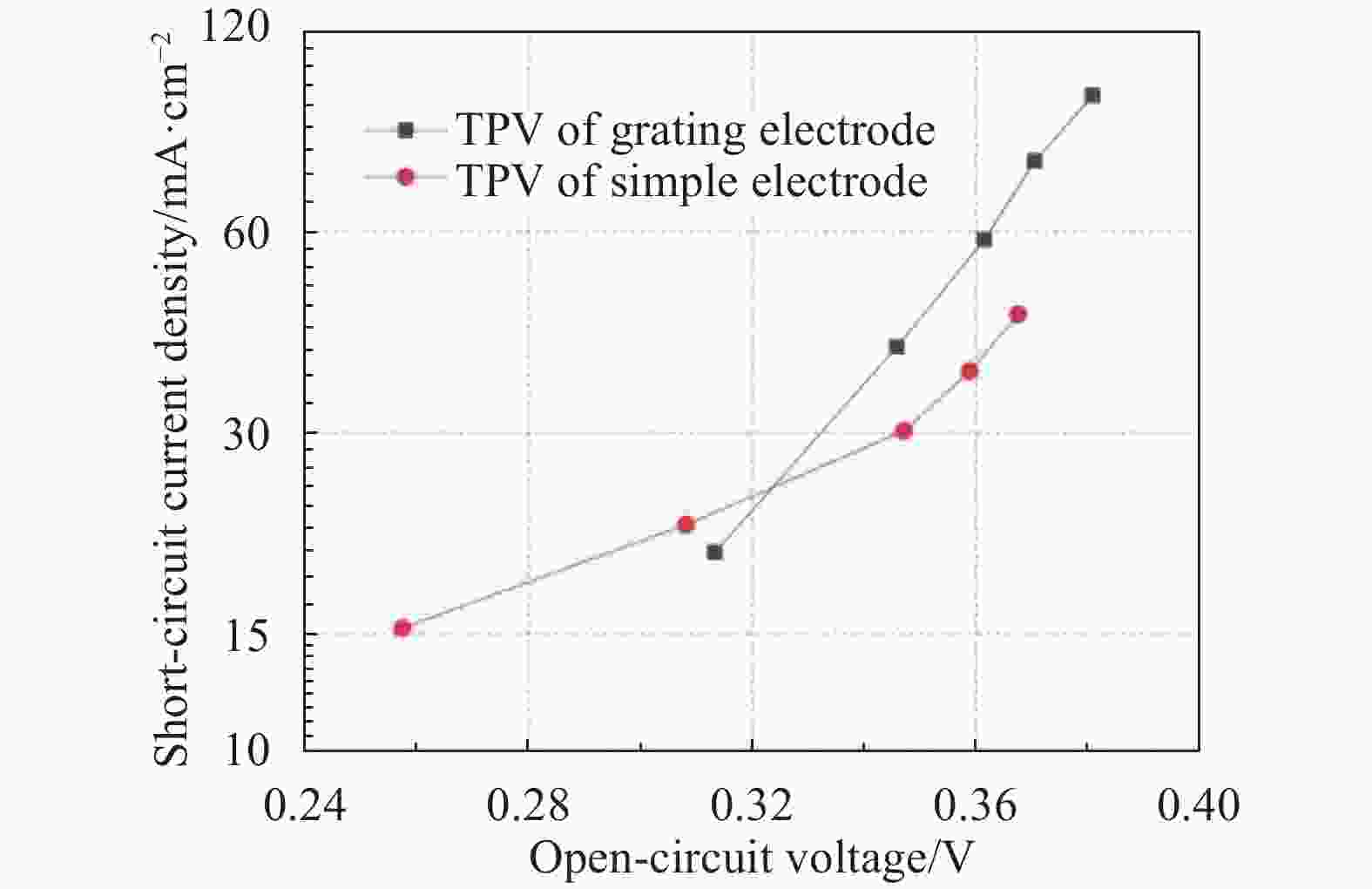
Figure 10. Comparisons of the short-circuit current density versus the open-circuit voltage for the TPV cells
As can be seen from the above figures, the TPV cell with a grating electrode has a higher short-circuit current density at all illumination levels compared to the TPV cell with a simple electrode. Analyzing the comparisons of the short-circuit current density versus the open-circuit voltage for the TPV cells, we can find that at the same illumination levels, the grating electrode greatly improves the short-circuit current density.
By analyzing the differences between the two kinds of GaSb TPV cells, we can find the influence of the electrode shape. The two kinds of GaSb TPV cells have the same epitaxial structure and technological process. The only difference between the two kinds of GaSb TPV cells is the shape of the electrode. One is the grating electrode and the other is the simple electrode. Therefore, different performance can be seen as the result of the different electrode shape. Compared with the simple electrode, the grating electrode has extra area which reduces the light area by 4%. Nevertheless, the GaSb TPV cell with the grating electrode still has much higher short-circuit current density.
Because of the distance between any two neighboring grating electrodes is 0.25 mm, the distance from any point on the cell surface to the electrode is less than 0.13 mm for the grating electrode. But for the simple electrode, the maximum distance is more than 2.4 mm. Obviously, the grating electrode has reduced the lateral distance by more than ten times.
On the one hand, it takes a lateral distance for the photo-induced carriers to reach the electrode. The lateral distance of the grating electrode is much shorter than that of the simple electrode. Therefore, much less time is needed for the photo-induced carriers to reach grating electrodes, which greatly reduces the probability of carrier recombination. The regularity of photo-induced carriers changing with time is given as
The less time means the less probability of the carrier recombination. As taking less time, the number of photo-induced carriers collected is greatly increased. Compared with the simple electrode, the grating electrode can collect more photo-induced carriers, and greatly improves the short-circuit current density.
On the other hand, the shorter lateral distance means shorter lateral transportation of the photo-induced carriers. It will greatly reduce the resistance from the active region to the electrode. The equivalent series resistance(Rs) consists of the resistance from the emitter to the electrode(Relectrode) and the other resistance(Rleft) that is given as
Considering that the two kinds of GaSb TPV cells are different only in electrode structure, the Rleft of the TPV cells are the same. The less Relectrode means that the grating electrode greatly reduces the Rs of the TPV cells. The reduction of the equivalent series resistance will improve the short-circuit current density.
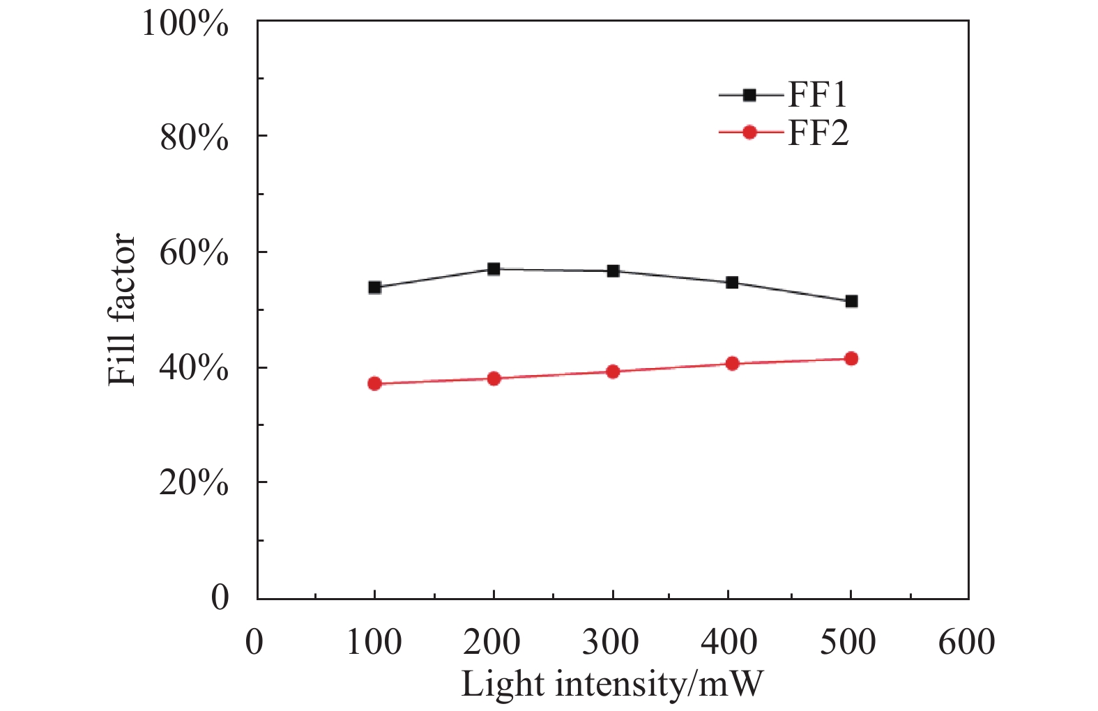
Figure 11 shows the relationship of the fill factor with the incident light intensity for the GaSb TPV cells. The curve of FF1 represents the TPV cell with a grating electrode and the curve of FF2 represents the TPV cell with a simple electrode. Obviously the fill factors of the TPV cell with a grating electrode are higher than that of the TPV cell with a simple electrode.

Figure 11. Fill factor of the GaSb TPV cells
As can be seen from the Fig.11, the fill factors of the TPV cell with a grating electrode are all above 50%. It is concluded that the grating electrode greatly improves the fill factor. On the one hand, the grating electrode will greatly increase the number of the photo-induced carries. Therefore, the grating electrode greatly improves the short-circuit current density, which means higher fill factor. On the other hand, the grating electrode reduces the resistance from the emitter to the electrode. It means that the grating electrode greatly reduces the equivalent series resistance of the TPV cells. Among the parameters affecting the performance of photovoltaic cells, the equivalent series resistance and the equivalent parallel resistance have greatest influence on fill factor. The larger the equivalent series resistance is, the smaller the filling factor is. Therefore, the grating electrode greatly reduces the equivalent series resistance of the TPV cells means the grating electrode will improve the fill factor. An optimal fill factor, as high as 56.8%, has been achieved. And we have obtained the highest photoelectric conversion efficiency which is up to 3.96%. At home, there is little research on GaSb TPV cells, especially large-area GaSb TPV cells. For small area GaSb TPV cells, the best device performance is 0.22 V of open-circuit voltage and 46.9% of fill factor[15], which is lower than this paper’s. In foreign countries, the photoelectric conversion efficiency of GaSb TPV cells is as high as 6%[16], which is higher than this paper’s. But the open-circuit voltage and the short-circuit current density of the proposed GaSb TPV cells are significantly higher than the device performances reported before [17].
-
In this work, we report the growth and characterization of GaSb TPV cells. The GaSb TPV cells were grown on GaSb substrates using MBE method. And two kinds of TPV cells with 1 cm×1 cm dimensions that have different electrode shape were fabricated. Compared with the TPV cell that has a simple electrode, the TPV cell that has a grating electrode shows better device performance including open-circuit voltage, short-circuit current density, fill factor and photoelectric conversion efficiency. Under one-sun illumination, the TPV cell with a grating electrode exhibits an open-circuit voltage of 0.303 V and a short-circuit current density of 27.1 mA/cm2. And the TPV cell with a simple electrode exhibits an open-circuit voltage of 0.235 V and a short-circuit current density of 16.6 mA/cm2. Under infrared light illumination, the TPV cell with a grating electrode exhibits an optimal fill factor of 56.8% and a highest photoelectric conversion efficiency up to 3.96%. Considering that the two kinds of GaSb TPV cells are different only in electrode structure, the improvement of the devices performance can be regarded as being caused by the difference of the electrode structure. In conclusion, the grating electrode is helpful to improve the short-circuit current density and fill factor for TPV cells.
Research on character of molecular beam epitaxial GaSb thermophotovoltaic (TPV) cells
doi: 10.3788/IRLA20200224
- Received Date: 2020-06-08
- Rev Recd Date: 2020-10-20
- Available Online: 2021-05-12
- Publish Date: 2021-03-15
-
Key words:
- GaSb /
- thermophotovoltaic (TPV) cell /
- open-circuit voltage /
- short-circuit current density /
- fill factor
Abstract: GaSb thermophotovoltaic cells were epitaxially grown on GaSb substrates by the Molecular Beam Epitaxy (MBE) method. And two kinds of GaSb TPV cells with 1 cm×1 cm dimensions that had different electrode shape were fabricated. In order to obtain high quality GaSb epitaxial layer, the growth conditions of MBE were optimized continuously. The quality of epilayers was good which was shown in the surface morphology characterized by AFM. The root mean square (RMS) of surface morphology was only 1.5 Å (1 Å=0.1 nm). Device characteristics including open-circuit voltage, short-circuit current density, external quantum efficiencies, fill factor and dark current density of the TPV cells were measured and compared. Under solar simulation, the TPV cells exhibited an open-circuit voltage of 0.303 V and a short-circuit current density of 27.1 mA/cm2. Compared with the TPV cell that had a simple electrode, the TPV cell having the grating electrode showed better performance in short circuit current density and fill factor. Under infrared light illumination, the TPV cell with a grating electrode exhibited an optimal fill factor of 56.8%.


 DownLoad: