


-
在MOS晶体管中,掺杂物的扩散始终是影响器件性能的重要因素,在离子注入工艺完成后的退火工艺过程中,硅中的掺杂物原子在高温作用下向周围扩散,导致硅掺杂与预期出现偏差,这就导致晶体管的性能发生变化[1]。瞬间增强扩散(transient enhanced Diffusion, TED)是较小的杂质离子(比如,硼、磷等)在高温过程中通过间隙原子或空穴的帮助发生的快速的离子扩散运动[2]。这种增强扩散是在短时间内发生的,并在一定时间后达到饱和状态,离子的扩散距离很大,杂质离子分布状况发生很大改变,影响器件性能[3]。1973年,Hofker[4]等人首次报道了硅中硼离子的TED现象,硼离子的最大扩散距离超过了200 nm,而普通的离子热扩散距离是3~5 nm。经过各国学者多年的研究,TED效应的原理和机制已经解释清楚,也提出了很多抑制方法,包括快速热退火(RTA)技术[5]、引入陷阱层[6]、沟道后注入[7]、oxygen-inserted silicon技术[8]等。随着器件尺寸进入亚微米领域,TED效应导致的离子再分配问题无法忽略,严重影响了晶体管性能,文中深入研究了沟道中硼离子TED效应导致的阈值电压漂移与沟道尺寸的关系,通过离子注入实验和TCAD仿真解释探究沟道内离子分布情况。
-
硅中掺杂杂质的热扩散分为直接扩散和间接扩散两种机制,其中直接扩散所需要的激活能很高,发生概率很低,间接扩散是由点缺陷引起的替位原子的热扩散,几种扩散表达式如下:
式中:A表示掺杂原子;V表示空穴;I表示间隙原子;As表示替位原子;AI表示处于晶格间隙的掺杂原子。公式(1)和(2)是一般情况下硅中掺杂原子的扩散方式,替位原子与空穴或间隙原子结合,仍然处于晶格位置。公式(3)称为Frank-Turnbull机制,一个替位原子在高温下运动到晶格间隙,产生一对间隙杂质原子和空穴。公式(4)称为“kick-out”机制[9],在间隙硅原子的作用下,晶格位置的替位原子运动到晶格间隙成为间隙杂质原子,而间隙硅原子占据晶格位置。“kick-out”机制是硅中掺杂离子发生TED的机制。硼和磷都会发生TED 效应,但硼的扩散速度比磷要快[10],所以相比于PMOS,沟道掺杂杂质为硼的NMOS晶体管表现出更明显的TED效应,图1是NMOS和PMOS晶体管阈值电压Vt随沟道长度L变化的曲线,NMOS晶体管曲线存在拱起,反短沟道效应[11](RSCE)十分明显。
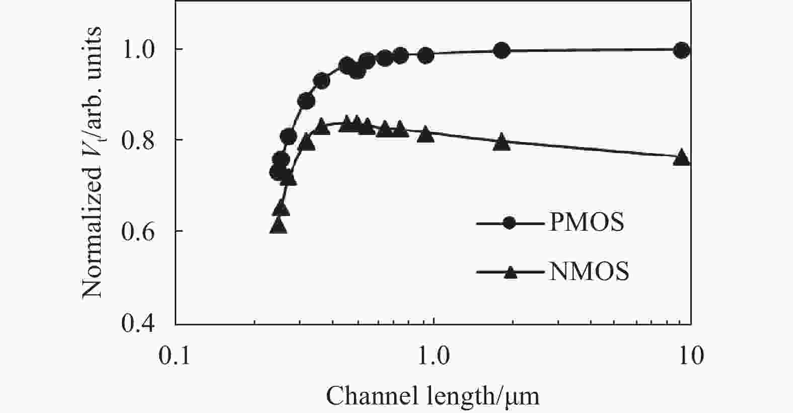
Figure 1. Comparison diagram of Vt-L curve of NMOS and PMOS transistor
间隙硅原子通常是由离子注入[12]和硅晶体表面氧化[13]过程产生的,氧化过程引入的间隙原子相比离子注入要少得多。离子注入工艺会造成晶体损伤,产生很多缺陷,需要采用退火工艺来修复损伤,但是也会形成新的二次缺陷。{311}缺陷与TED效应具有紧密联系,{311}缺陷是一种特殊的间隙原子型缺陷,间隙原子团簇捕获间隙原子形成<110>间隙原子链,沿着<233>方向排列,并延伸生长最终形成稳定的{311}缺陷[14],只有当掺杂杂质注入剂量大于5×1013 cm−2时,才会形成{311}缺陷。在800 ℃以上高温的退火过程中,{311}缺陷分解释放出大量的间隙原子,这些间隙原子帮助沟道内的硼离子进行增强扩散。退火温度也会影响TED效应,当温度超过1 000 ℃时,由于退火的活化能(约为5 eV)高于扩散的活化能(3~4 eV),退火过程比扩散过程快一些[15],TED效应减弱。800 ℃是硅中硼离子的TED效应最严重的温度,饱和时间约为1 h。
-
在晶体管中引入碳陷阱层是抑制TED效应的有效方法,碳陷阱层可以吸收过剩的间隙原子,避免其帮助杂质原子扩散[16]。间隙原子通过“kick-out”机制取代晶格位置的碳原子,而处于晶格间隙可移动的碳原子与替位碳原子形成不可移动的碳原子团,捕获间隙原子和形成原子团的两步反应式如下[17-18]:
式中:Cs为处于晶格位置的碳原子;CI为处于晶格间隙的碳原子;(CsCI)为不可移动的碳原子团,并且碳原子团会变得更大。碳陷阱层通常采用预非晶化掺杂、LDD协同注入的方式形成,需要高浓度的注入剂量保证充分吸收间隙原子。在抑制TED的同时,还可以有效抑制隧道效应,减少离子注入的射程末端EOR (End-of-Range,EOR)缺陷。
-
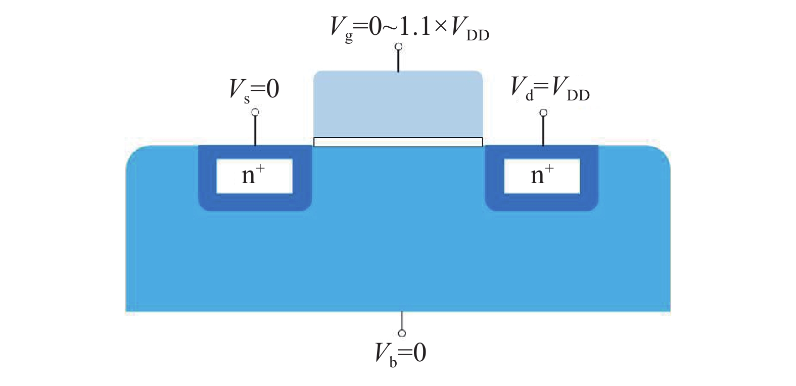
文中测试所用的晶体管采用40 nm CMOS工艺,在300 mm <100>晶圆上制造,隔离工艺是浅沟槽隔离(shallow trench isolation,STI)。在器件制造完成后,进行晶片允收测试(wafer acceptance test,WAT),收集晶体管电性能参数,包括阈值电压Vt、饱和漏电流Idsat、衬底电流Isub等,主要对阈值电压的漂移问题进行详细研究。阈值电压的测试方法如图2所示,其中,VDD=1.8 V,衬底电压Vb和源极电压Vs为0 V,栅极电压Vg从0开始扫描直到1.1×VDD,实时测量漏电流Id,当Id=0.1 μA ×(W/L)时,栅极电压即为阈值电压。

Figure 2. Schematic diagram of Vt measurement method
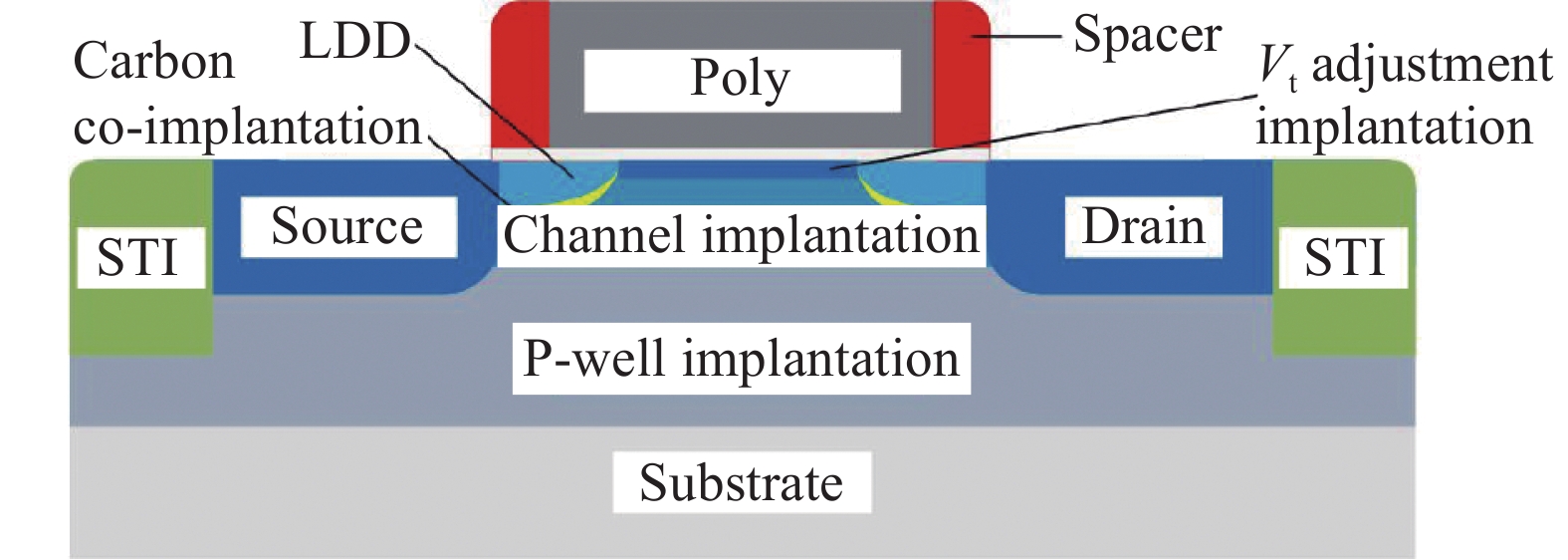
器件内的杂质离子分布情况十分复杂,因为注入的离子种类多样,注入条件也各不相同,通常CMOS工艺中MOS晶体管各部分形成顺序是:STI−沟道−多晶硅栅−源/漏−金属层,图3是现代NMOS晶体管结构及前段工艺示意图,离子注入工艺顺序是:P阱离子注入−沟道离子注入−调阈值注入−低掺杂漏极(LDD)离子注入−LDD碳协同注入−源/漏离子注入。
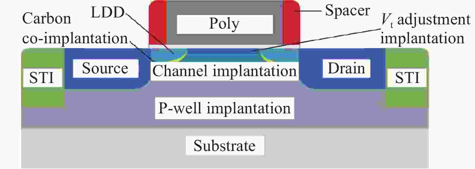
Figure 3. Schematic diagram of MOSFETs structure and process
按照顺序依次进行实验,改变离子注入能量和剂量,对比晶体管阈值电压曲线。现代CMOS工艺采用LDD结构,在沟道中靠近漏极的附近设置一个低掺杂的漏区,克服热载流子效应,也属于漏极的一部分。因为硼TED发生在离子注入射程末端,主要影响沟道表面的硼离子分布,所以对调阈值注入、LDD离子注入和LDD碳协同注入进行分批实验,再对高温炉退火和红外快速热退火工艺进行对比实验。采用Sentaurus TCAD工具进行工艺仿真,并将实际生产中的器件WAT参数作为反馈输入到模型中,使模型更加精确。
-
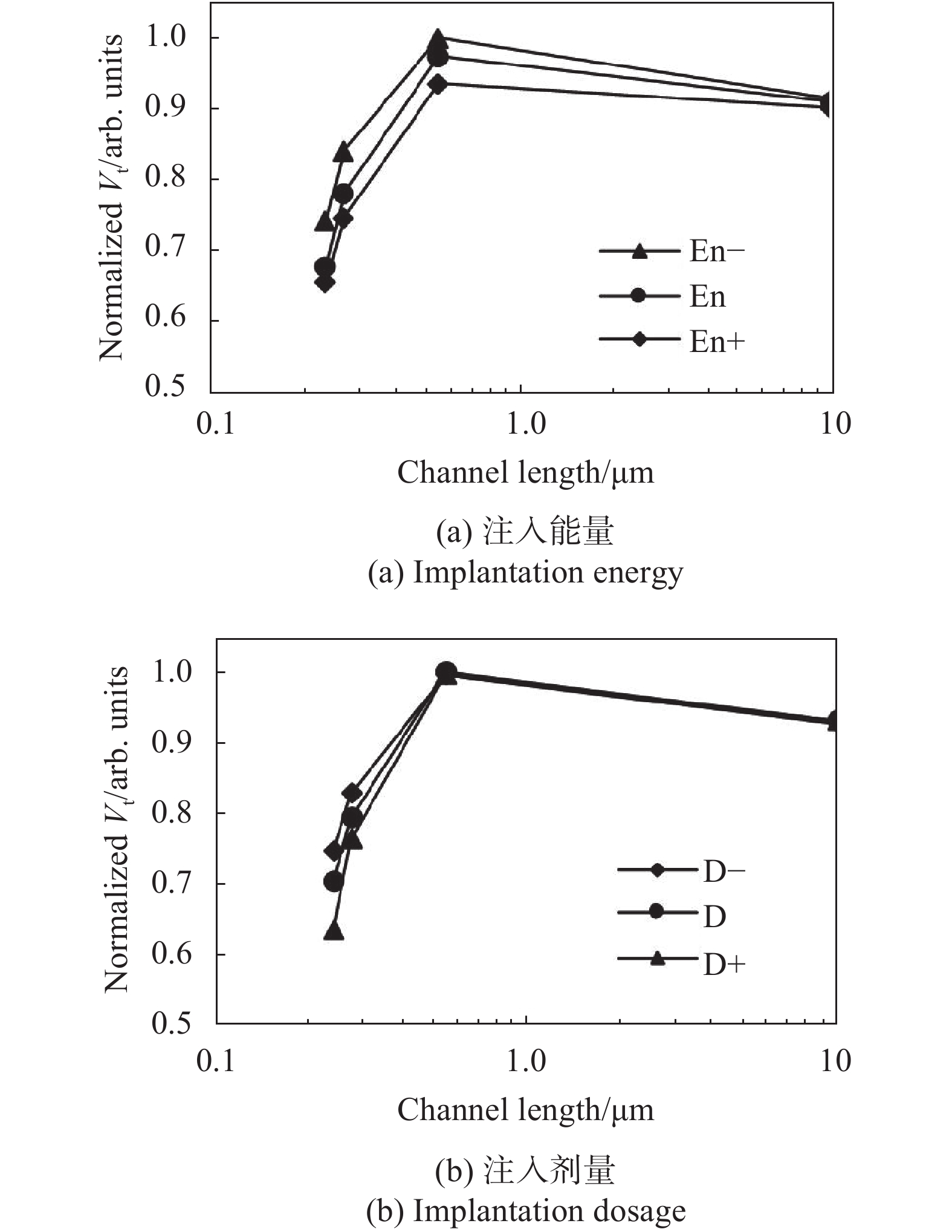
测量相同工艺条件下不同尺寸的晶体管阈值电压,以沟道长度L为横坐标,阈值电压为纵坐标绘制曲线,如图4所示,对调阈值离子注入能量和剂量进行调整,“En、En+”表示注入能量逐渐增强,“D−、D、D+”表示注入剂量逐渐增加,“跳过”表示取消这一道离子注入工艺。图中纵坐标的阈值电压值都经过归一化处理。沟道长度分别为10 μm、0.55 μm、0.27 μm和0.24 μm,沟道宽度为10 μm。曲线拱起程度代表TED影响的强弱。调阈值注入的离子是硼,能量和剂量的改变是曲线整体偏移,斜率变化很小,表明硼的TED效应没有受到影响。注入能量提高,注入深度会增大,表面杂质浓度变低,阈值电压也就降低。注入剂量提升,阈值电压也随之上升。由于NMOS晶体管沟道形成需要多道硼离子注入工艺,硼离子浓度比较高,TED效应达到饱和[19]。
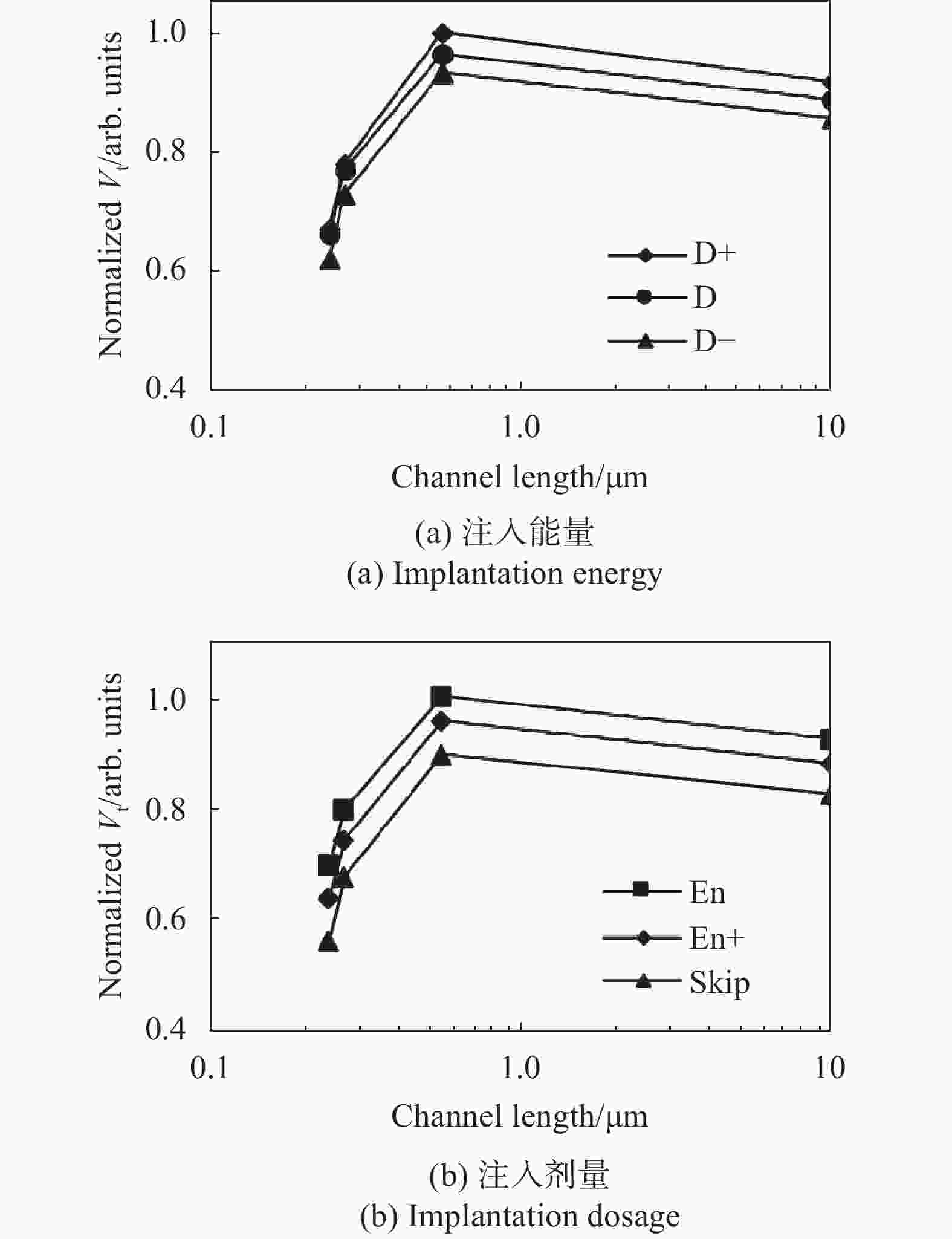
Figure 4. Vt-L curves of Vt adjustment ion-implantation experiments
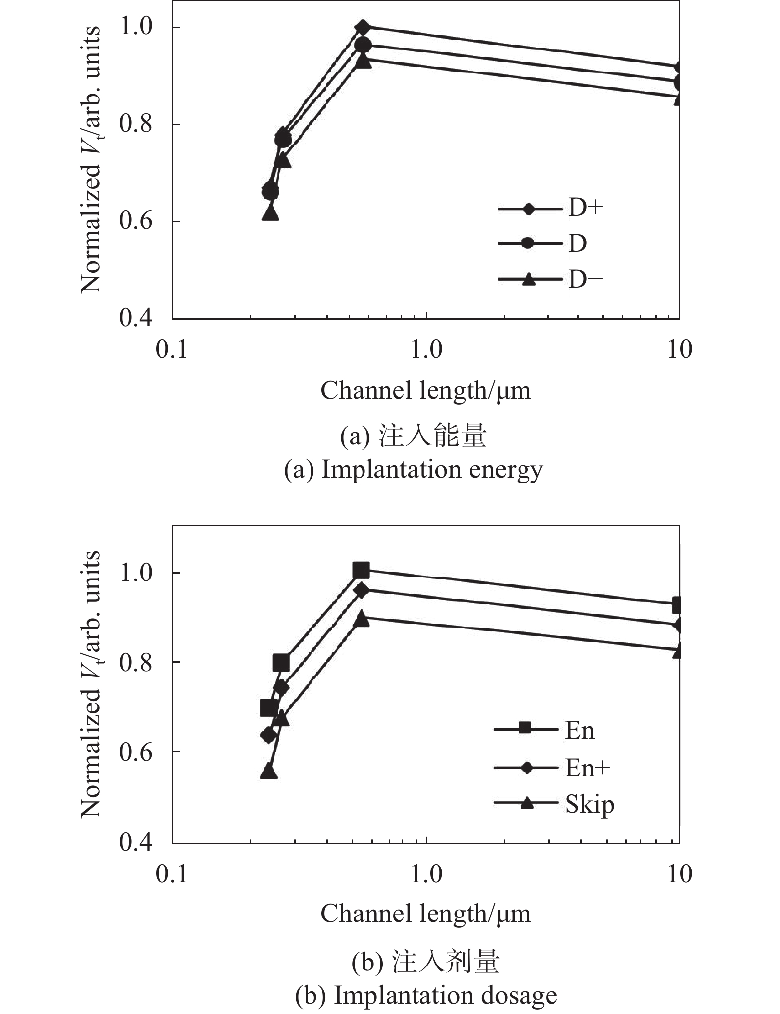
LDD离子注入分为两步:磷离子注入和砷离子注入,先注入磷离子后注入砷离子,砷离子注入能量比较低,在硅衬底表面形成浅结。图5是LDD两道离子注入的实验结果,图(a)和(b)分别是磷离子注入能量和剂量实验,图(c)和(d)分别是砷离子注入能量和剂量实验。沟道长度分别为10 μm、0.55 μm、0.27 μm和0.24 μm,沟道宽度为10 μm。砷离子注入能量和剂量的改变对阈值电压没有影响,因为砷掺杂区域被磷离子掺杂区域包围,对沟道几乎没有影响。而磷离子注入条件的改变对阈值电压的影响主要体现在短沟道区域,能量和剂量越高,阈值电压越低。高温下,LDD会向沟道区域扩展,磷离子浓度的改变导致LDD向沟道扩展程度的改变[20],有效沟道长度(L−ΔL)发生变化,当沟道长度L比较大时,ΔL远小于L,可以忽略,只有在沟道比较短时,ΔL不可忽略,短沟道效应导致阈值电压下降。磷离子注入能量越高,剂量越大,LDD向沟道扩展越多,有效沟道长度越小,阈值电压越低。LDD磷离子注入条件改变对沟道内硼的增强扩散基本没有影响。
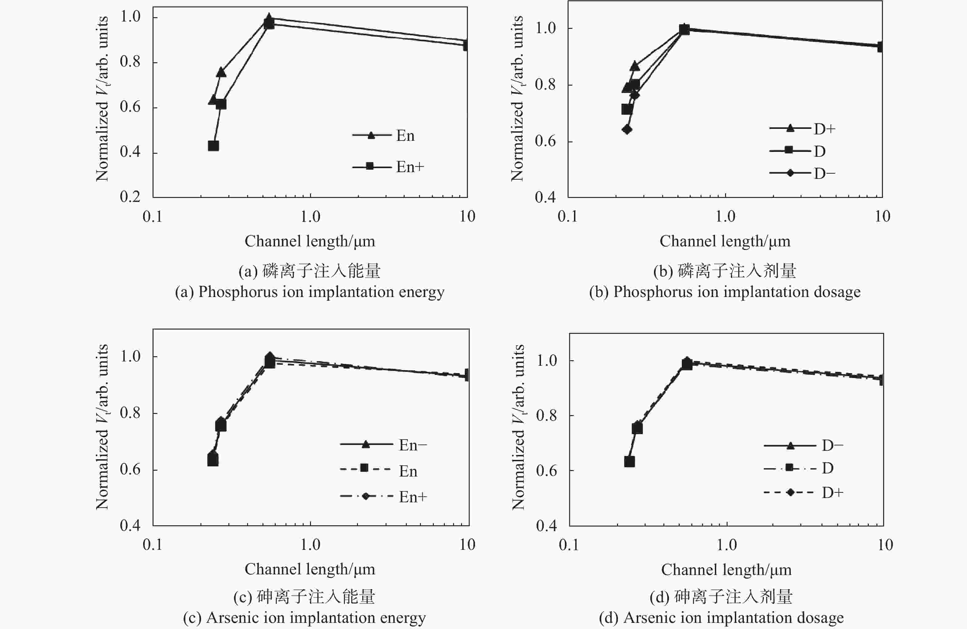
Figure 5. Vt-L curves of LDD ion-implantation experiments
图6是LDD碳离子协同注入实验结果,其中,图(a)和(b)分别是注入能量和剂量的实验曲线图。沟道长度分别为10 μm、0.55 μm、0.27 μm、0.24 μm,沟道宽度为10 μm。注入能量对硼TED的影响比较明显,能量越高,曲线的拱起程度越低,TED效应受到抑制。形成碳陷阱层需要高剂量的碳离子注入,在1014 cm−2以上,调整幅度较小的情况下,剂量改变产生的影响并不明显。在这六组实验中,曲线的最高点都在沟道长度约为0.55 μm的位置,硼TED效应对阈值电压的影响达到最大,L>0.55 μm,TED占据主导,阈值电压一直上升,L<0.55 μm,TED的影响减弱,阈值电压开始下降。

Figure 6. Vt-L curves of LDD carbon ion co-implantation experiments
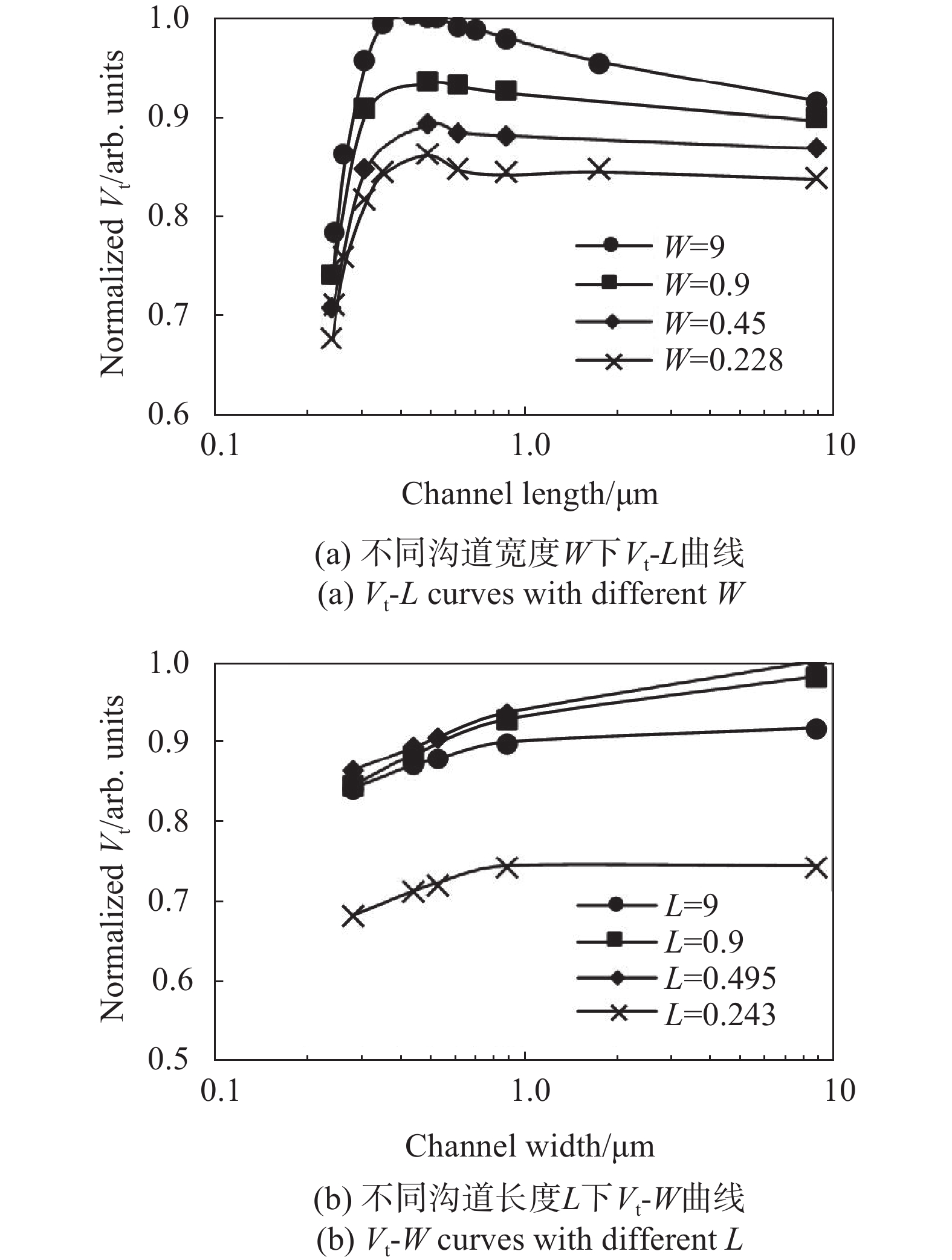
器件尺寸对TED效应存在一定的调控作用,将不同沟道长度和宽度的晶体管阈值电压进行对比,图7(a)是不同沟道宽度下的Vt-L曲线,随着沟道长度的减小,阈值电压先上升后下降,沟道宽度越小,阈值电压越低,并且L>0.55 μm区域的曲线斜率也越小,TED效应的影响变弱。图7(b)是不同沟道长度下的Vt-W曲线,阈值电压随着沟道变窄一直下降,窄沟道区域的曲线斜率增大。L=0.495 μm时,阈值电压最高,曲线斜率也最大,其次为L=0.9 μm的曲线,L=0.243 μm的曲线最低,与Vt-L曲线相符合。

Figure 7. Vt curves with different channel sizes
-
传统的高温炉退火技术需要30 min~1 h的时间才能完成,温度在1 000 ℃以下,扩散过程比退火过程更快,而且有足够的时间发生增强扩散,沟道中的硼离子的TED效应显著。红外快速热退火技术是单晶圆工艺,升温速度快,晶圆受热均匀,可以在10 s内将晶圆温度由室温提升到1 000 ℃以上,并且可以精确控制晶圆的温度和晶圆内的温度均匀性。当温度达到1 100 ℃时可以在10 s左右恢复硅的单晶结构,在1 000 ℃以上退火的活化能高于扩散的活化能,退火过程比掺杂原子扩散过程快一些,因为退火时间极短,沟道内的硼离子没有足够的时间完成增强扩散,所以TED效应得到了有效抑制。快速退火系统采用钨卤素灯来进行加热,利用红外辐射产生密集的热量,晶圆的温度可以用红外线高温计准确测量。
图8是分别采用高温炉退火和红外快速热退火技术的晶体管阈值电压曲线,其中高温炉退火温度为900 ℃,时间为30 min,红外快速热退火温度为1 050 ℃,时间为15 s。代表红外快速热退火的曲线斜率更低,表示TED效应得到有效抑制。

Figure 8. Vt curves with different annealing process
-
使用集成工艺仿真系统Sentaurus Process模拟器件的制造过程,对每一步工艺进行仿真,包括刻蚀、离子注入、光刻等,建立模型,然后根据实际生产测试数据对模型进行校准,得到准确的仿真模型,输出晶体管从沟道中心到漏端的硼离子和间隙原子浓度分布曲线。图9是不同碳注入能量下的TCAD工艺仿真结果,图(a)是沟道表面硼离子浓度分布曲线,图(b)是间隙原子浓度分布曲线。碳离子注入能量越高,硼离子浓度和间隙原子浓度越低。沟道中心硼离子浓度最低,在靠近边界的位置浓度陡然升高,在边界处达到最高,TED导致的硼离子聚集主要发生在沟道和LDD的边界位置。间隙原子浓度分布表明:硼TED所需的间隙原子来自于LDD离子注入,间隙原子从LDD向沟道扩散,越靠近沟道中心,浓度越低,导致边界处出现硼浓度峰。当沟道长度缩短时,沟道两侧的硼离子浓度峰靠近,表面平均硼离子浓度升高,阈值电压也就随之升高,当两侧边界的浓度峰接触时,硼的聚集效应达到最大,TED对阈值电压的影响也达到最大,此时的沟道长度约为0.55 μm,沟道长度继续缩短,硼离子浓度也不能再增加,反而由于短沟道效应,阈值电压开始下降。

Figure 9. TCAD simulation result
-
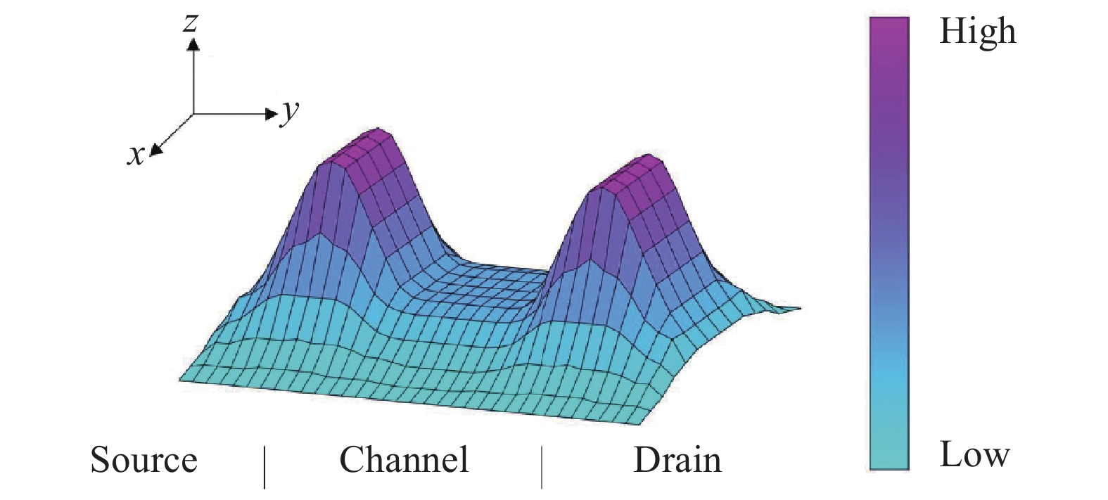
在沟道长度方向上硼离子聚集的同时,在宽度方向上,因为TED效应聚集的硼离子却会向STI中扩散[21],STI边界硼离子浓度降低。STI工艺代替局部氧化硅LOCOS(Local Oxidation of Silicon, LOCOS)工艺形成有源区之间的隔离,具有更好的隔离性能,而且表面积更小,为集成电路节省面积,现在已经广泛应用于集成电路制造工艺中。但是由于其具有尖锐角落的陡峭沟渠[22],使得STI和源/漏区形成的角落成为沟道中扩散的杂质离子的聚集地,NMOS晶体管沟道中的硼离子因TED效应聚集在角落并泄漏到STI区域,所以靠近角落的区域硼离子浓度比较高,角落处反而很低。图10是NMOS器件发生TED效应后沟道内的硼离子浓度分布示意图,x轴方向是沟道宽度方向,y轴方向是沟道长度方向,颜色越深表示浓度越高。两侧的浓度峰是LDD-沟道边界,STI与LDD形成的四个角落和STI-沟道边界硼浓度最低。

Figure 10. Schematic diagram of boron ion concentration distribution in devices with TED
TED效应聚集了大量的硼离子,加速了STI对硼离子的吸收,沟道宽度比较大时,可以忽略这些被STI吸收的硼离子对阈值电压的影响,但当沟道宽度不断减小,被STI吸收的硼离子越来越多,STI边界硼离子浓度降低的区域占据沟道的比例上升,根据理想阶梯状分布模型[23],阈值电压方程为:
式中:
${\gamma _1} $ 为体因子或体效应系数,与制造工艺相关,Vfb为平带电压;Vsb为体偏压;${\phi _{\rm f}}$ 和${\phi _{\rm Si}}$ 分别为费米势和硅表面势;Ns为掺杂浓度。Ns降低,阈值电压也就不断降低。沟道宽度减小还会导致LDD边界硼浓度峰的降低,TED效应对阈值电压的影响就会减弱。 -
TED效应导致硼离子在沟道-LDD边界聚集和在STI边界泄漏,两者同时影响硼离子的浓度分布。硼离子浓度变化均在沟道边界位置,所以阈值电压漂移程度受沟道尺寸的调控,当沟道长度缩短时,硼的聚集效应增强导致阈值电压升高,在L=0.55 μm处达到最大,而沟道长度继续增大,TED效应不再占据主导因素。当沟道宽度W减小时,STI吸收作用导致阈值电压下降,TED效应加剧了STI对硼离子的吸收。两者对阈值电压的影响会相互抵消,窄沟道有利于降低TED效应的影响。采用高浓度的碳协同注入和红外快速热退火技术相结合的工艺可以有效抑制硼的TED效应。
Channel size-dependent TED effect in MOSFETs with infrared rapid thermal anneal
doi: 10.3788/IRLA20200306
- Received Date: 2020-12-10
- Rev Recd Date: 2021-01-15
- Publish Date: 2021-05-21
-
Key words:
- transient enhanced diffusion /
- threshold voltage /
- ion-implantation /
- channel size /
- interstitial Si /
- infrared rapid thermal anneal
Abstract: Boron transient enhanced diffusion (TED) causes reverse short channel effect, and threshold voltage (Vt) increases abnormally, which seriously affects the device performance and yield. The Vt increment is different with different channel size. To investigate channel impurity distribution and the influence of channel size on TED, Vt adjustment ion-implantation, LDD ion-implantation and carbon co-implantation experiments were performed on 40 nm CMOS process, measuring Vt with different channel size and process, and using TCAD tools for process simulation. Experiments results show that Vt rises first with channel length decreasing and then drops sharply after reaching the maximum at 0.55 μm. The Vt -L curve slope decreases when channel width decreases. Vt decreases with channel width and it is decreasing faster and faster when channel length is constant. The interstitial Si atoms are injected by LDD ion-implantation and diffuse into channel, while boron pile up at the LDD-channel boundary. However, boron leak into the shallow trench isolation (STI) area at the corner formed by LDD and channel. Both pile-up and leakage control boron concentration distribution in channel. The Vt shift induced by boron TED is channel size-dependent, and high energy carbon co-implantation and infrared rapid thermal anneal can suppress TED effect effectively.


 DownLoad: