


-
ZnO is a promising candidate for UV photodetector applications due to its unique optical and electrical properties including direct wide band gap (3.37 eV), large exciton binding energy (60 meV) and strong resistance to high energy proton irradiation [1-5].Various ZnO nanomaterials have been used for fabrication of ultraviolet (UV) photodetector with high photoconductive gain and high responsivity [6–8]. However, these UV photodetectors suffered poor transient response (with response time up to minutes), which is attributed to surface defects and oxygen adsorption/desorption process of ZnO nanomaterials. Therefore, it is highly desirable to improve the transient response of ZnO nanomaterial for fast UV sensing.
By now, different methods have been developed to improve the transient response of ZnO based UV photodetectors, which include hydrogen doping, oxygen plasma treating, deposition of carbon nanotube network, and graphene shell coating [9–13]. Among all of them, the combination of graphene with ZnO is one of the most promising methods, as it can effectively improve the carrier transport and collection efficiency of ZnO based UV photodetectors, leading to a high responsivity and fast transient response [14-15].
In this work, we report a facile preparation method of the GQDs-ZnO nanowires UV photodetector for the first time by a simple spin-coating technique and low temperature vacuum annealing treatment method. GQDs-ZnO composites was synthesized using the Chemical Vapour Deposition (CVD) method for UV photodetector applications. By using the CVD method, the GQDs-ZnO composites achieved very high active surface to volume ratio, which is preferable for photocurrent generation. In addition, the high carrier mobility of graphene enabled efficient carrier transport and collection in the composite, leading to a high performance of this UV photodetector in terms of speed and photoresponsivity.
The attractiveness of this work lies in the simplicity of the treatment process, which could easily be scaled up, and paves the way for mass production of low-cost nanoscale UV photodetector. In addition, the fabricated device demonstrated a improved photocurrent under UV illumination in air at room temperature. This work represents a simple, clean, and efficient route to fabricate UV photodetector.
-
The fabrication of ZnO NWs. ZnO nanowires was grown on the SiO2/Si substrate in a horizontal tube furnace by chemical vapor deposition method. This system contains a quartz tube vacuum chamber 100 cm long and 10 cm in diameter. A mixture of the Zinc oxide powder (99.99%) and commercial nanodiamond powder (weight ratio 3∶1) were the precursor material. Before the quartz coat was inserted into the center of the quartz tube vacuum chamber, the precursor material was put into the coat and covered by the SiO2/Si substrate (1×1 cm2). And then, the precursor material were heated up to 960 °C with the high purity Ar gas (100 sccm) as the transfer gas. When the temperature was heated to the designed temperature, the high purity O2 gas (2 sccm) was introduced into the quartz tube and kept a fixed pressure (30 KPa) for 30 minutes. Finally, the ZnO sample could be obtained on the substrates after the chamber cooled down to the room temperature.
The fabrication of GQDs-ZnO Device. The GQDs modified ZnO nanowires were prepared using a spin-coating method. A few droplets of the GQDs solution (25 nm, Adrich-sigma) were deposited on the surface of ZnO nanowires with a rate of 1000 rpm for 20 s. And then, the substrate was heated at 140 ℃ for 15 mins to allow solvent evaporation. After that, the substrate was annealed at 500 ℃ for 20 mins in the vacuum quartz tube and then dispersed the substrate into ethanol with the help of ultrasound. Then, a droplet of the ZnO NW suspension is dropped over the interdigital microelectrodes of Au with digital spacing of 10 um, and then dried at 140 ℃ for 30 mins to vaporize the solvent, as shown in Fig. 1.

Figure 1. Fabrication process of ZnO-GQDs device
-
SEM was used to characterize the morphology of the products. Fig. 2 shows the SEM of the as-grown ZnO NWs and the GQDs-ZnO NWs. Fig. 2(a) and (b) show the top-view SEM images of the as-grown ZnO NWs and high-resolution images of the samples, respectively. From Fig. 2(b), we can find that the ZnO nanowires is the classical wurtzite sructure, and the diameter of ZnO nanowire is approximately 150 nm. Fig. 2(c) and Fig. 2(d) show the top-view SEM images of the GQDs-ZnO NWs and high-resolution images of the samples, respectively. From Fig. 2(d), we can find that the surface of ZnO nanowire is coated by the GQDs.
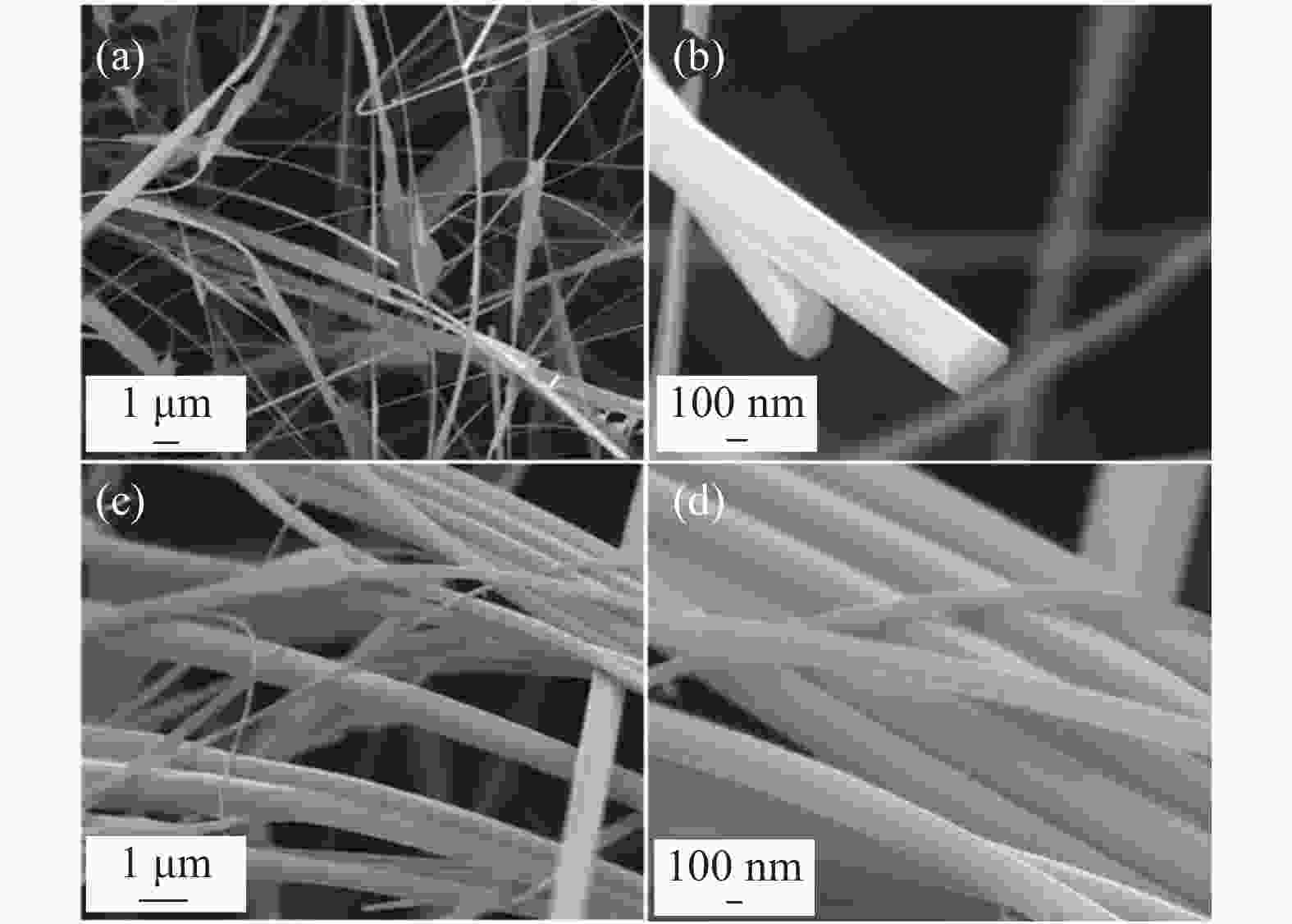
Figure 2. (a) Top-view SEM images of the as-grown ZnO NWs; (b) High resolution of ZnO NWs; (c) Top-view SEM images of the GQDs-ZnO NWs; (d) High resolution of GQDs-ZnO NWs
Figure 3 shows the transmission electron microscopy (TEM) of ZnO and GQDs-ZnO. The red circle in Fig. 3(a) and (c) are the observation regions of ZnO and GQDs-ZnO under transmission electron microscopy (TEM), respectively. Careful TEM observation of the GQDs-ZnO reveals that the interface of GQDs/ZnO nanowires has a great difference in Fig. 3(b) and (d), respectively. From Fig. 3(d), the broken regions in the surface of ZnO nanowire could be attributed to the GQDs reacted with ZnO nanowire under the vacuum environment.
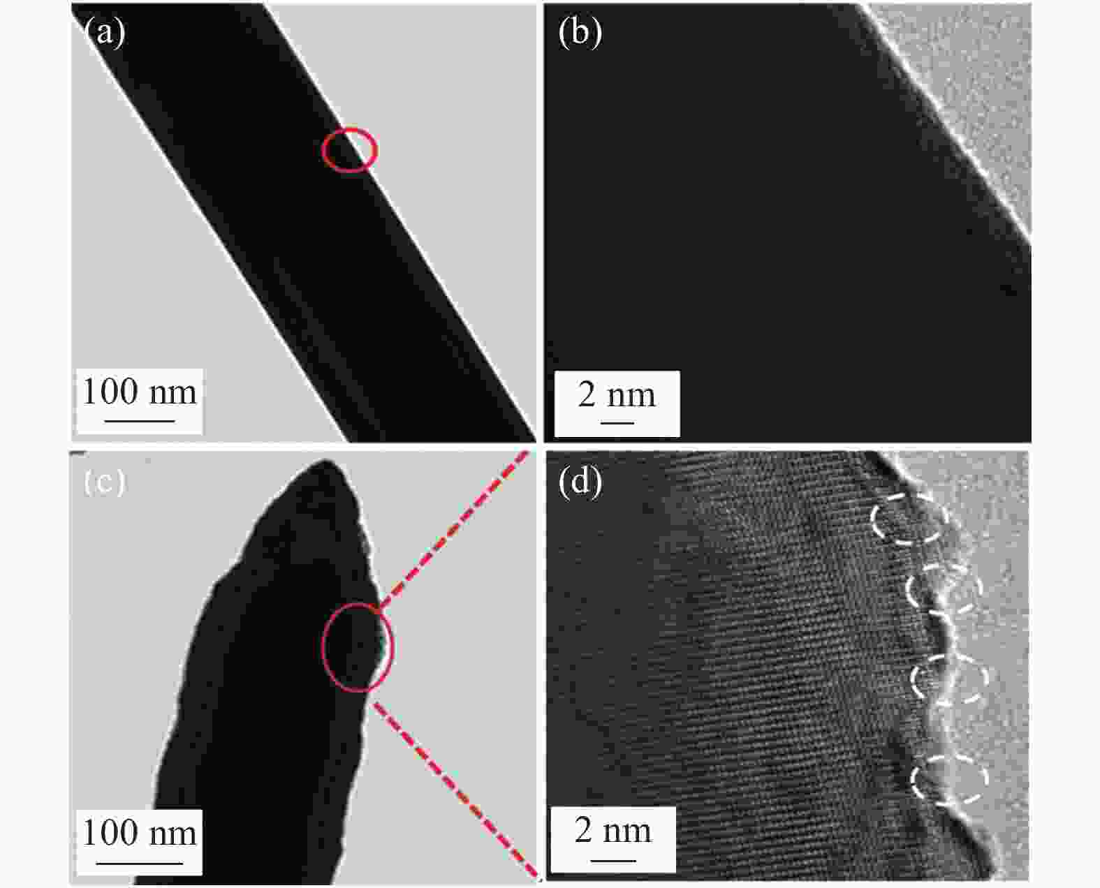
Figure 3. TEM of ZnO NWs and ZnO-GQDs NWs: (a) the single ZnO NW sample for TEM; (b) the observation regions of ZnO NW in red circle; (c) the single ZnO-GQDs NW sample for TEM; (d) the observation regions of ZnO-GQDs NW in red circle
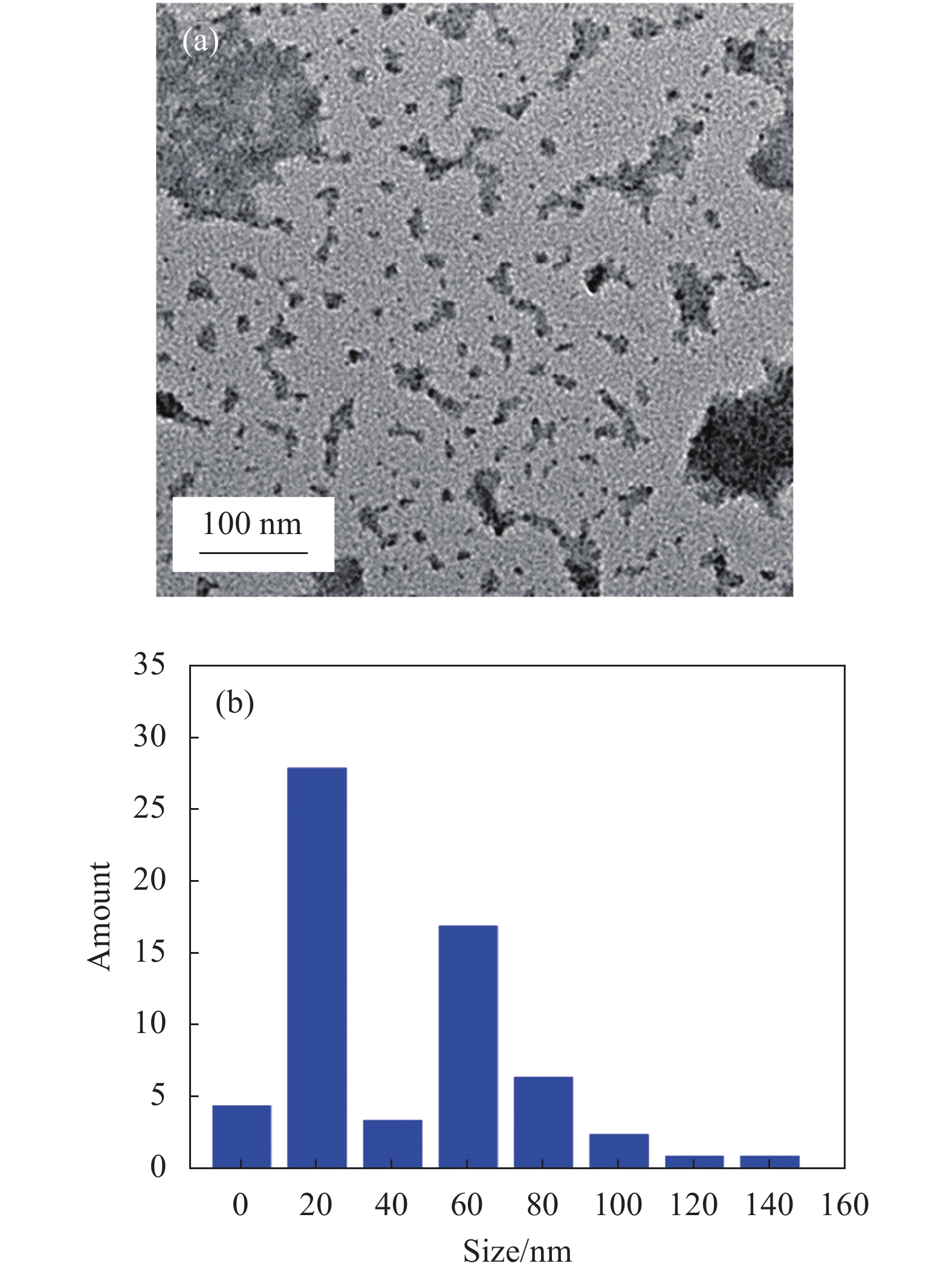
In order to characterize the GQDs diamerter, the GQDs’s TEM was made, as shown in Fig. 4. From Fig. 4(b), the most GQD’s diameter is 20 nm, and a few is 60 nm, and the rest size is very little.

Figure 4. GQDs’s diameter characterization. (a) the TEM of GQD; (b) the figure of diameter distribution statistics
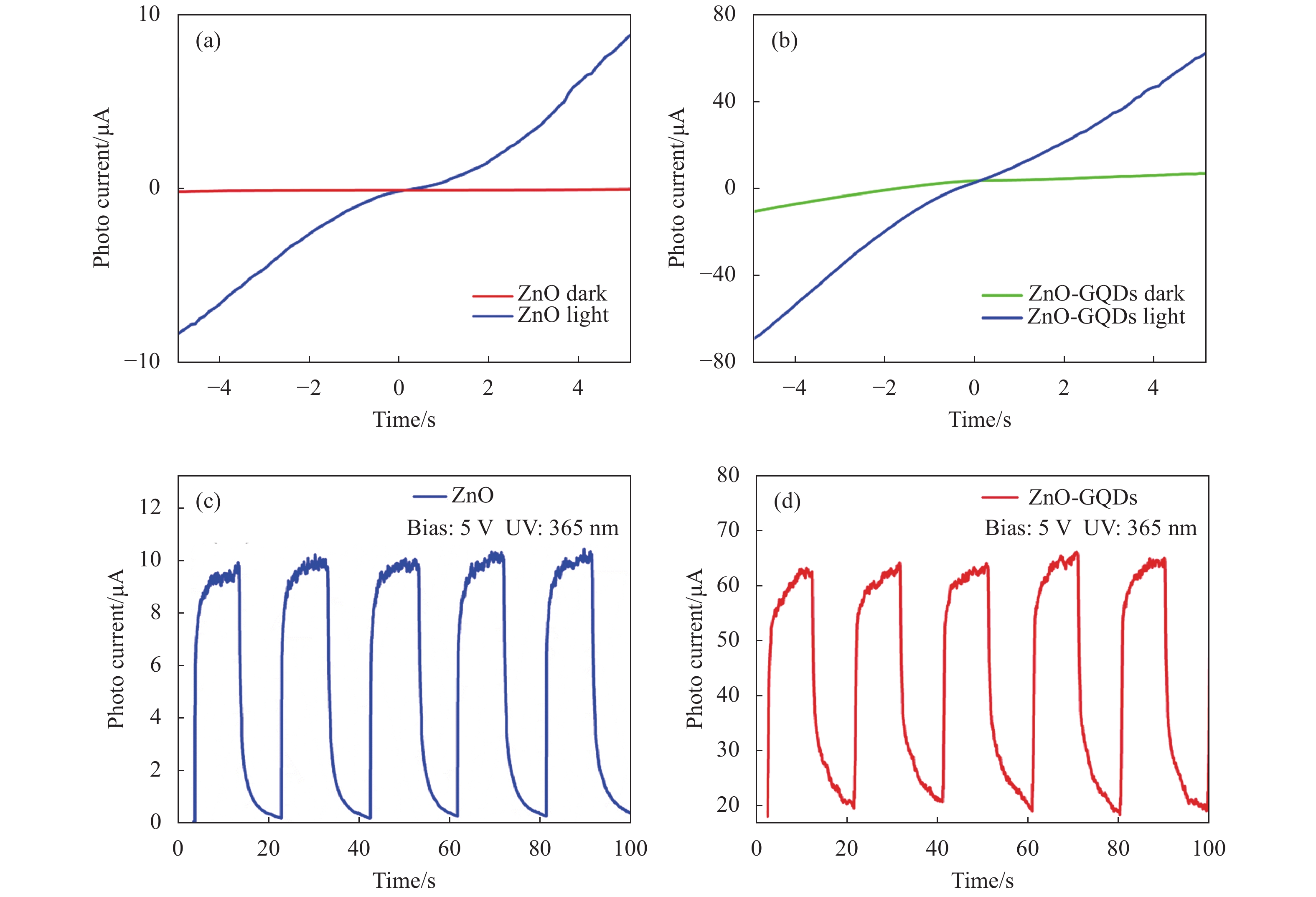
The photoresponse measurements of the device were carried out at ambient conditions with UV illumination (365 nm, 1.35 mW/cm2). The photoresponse behaviors of the ZnO NWs and GQD-ZnO NWs are shown in Fig. 5. Fig. 5(a) and (b) show the I-V cure of ZnO NWs and ZnO-GQDs, respectively. Fig. 5(c) and (d) show the I-T curves of ZnO NWs and ZnO-GQDs NWs, respectively. From Fig. 5, the photocurrent of ZnO-GQDs is larger than that of ZnO NWs. The increased photocurrent was a consequence of GQDs decorated the ZnO NWs surface, which led to an enhanced photocurrent.
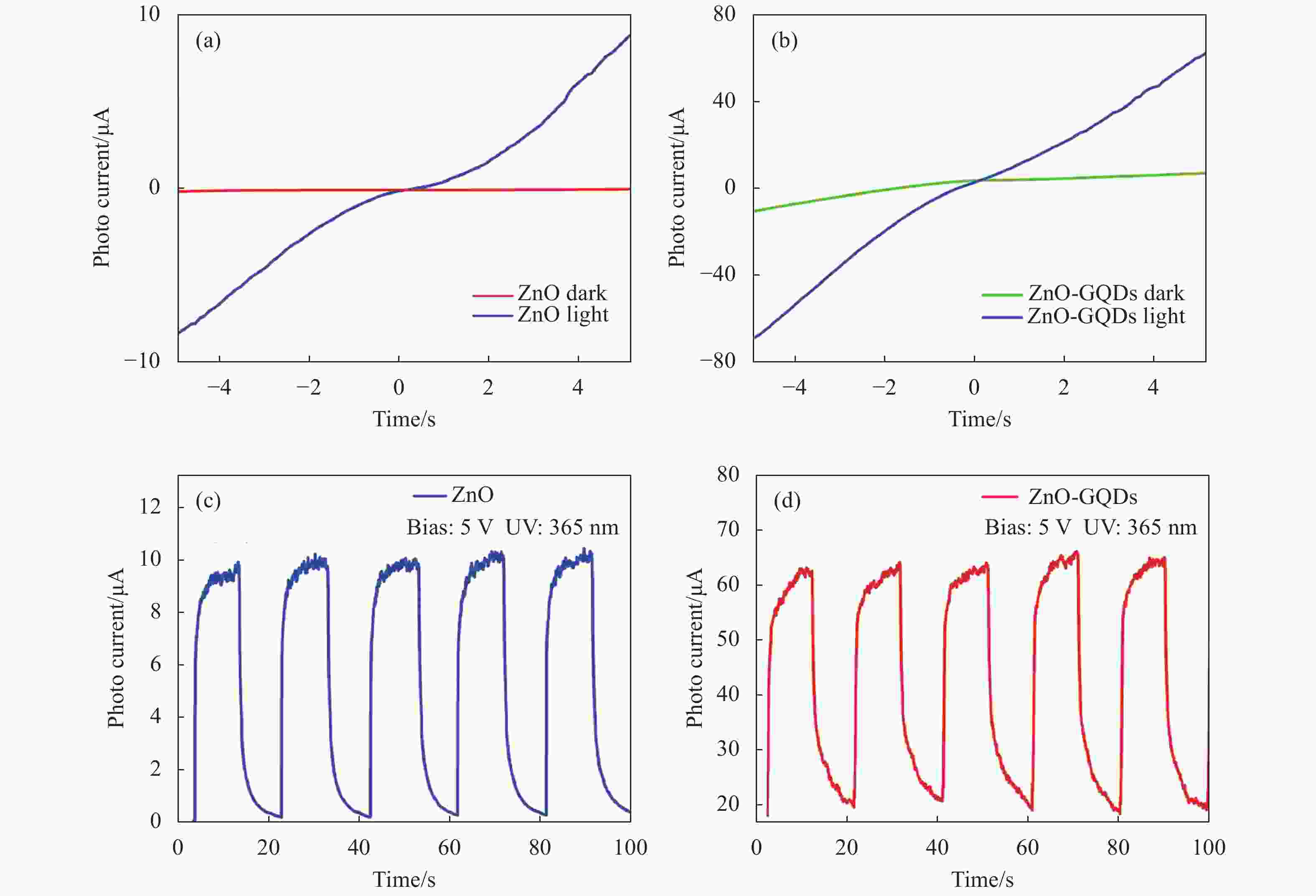
Figure 5. I-V characteristics of the ZnO NWs photodetectors (a) and ZnO-GQDs NWs photodetectors (b); I-T characteristics of the ZnO NWs photodetectors (c) and ZnO-GQDs NWs photodetectors (d)
According to an established mechanism[16], the electronic are captured by the adsorbed oxygen on the n-type ZnO nanowires surface, and under UV light illumination, the photogenerated holes are trapped, photodesorbing the adsorbed oxygen according to the consecutive steps: O2(g) + e− → O2− (ad) and h+ + O2− (ad) → O2(g) (as shown in Fig. 6(a)-(b)).
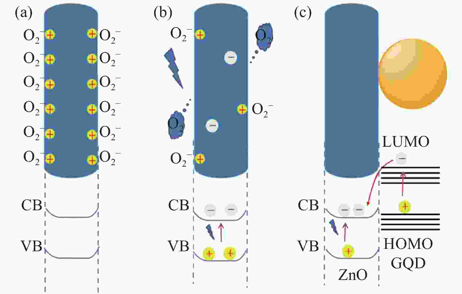
Figure 6. Photoresponse mechanism of the ZnO-NWs (a)–(b) and ZnO-G QDs (c). The oxygen plasma treatment improves the oxygen CB and VB are the conduction and valence bands, respectively
In ZnO-GQDs composites electron−hole pairs are generated in both ZnO nanowires and GQDs[17]. The holes migrate to the surface which facilitates the photodesorption process of adsorbed oxygen ions. The unpaired electrons, left behind after migration of photogenerated holes, enhance the free carrier concentration in the ZnO-GQDs composites and increase the photocurrent.
As a result post decoration of the ZnO nanowires with GQDs, the photocurrent increase compared to pristine ZnO nanowires.The mechanism can be explained by the schematic model in Fig. 6(c). Electron transfer occurs from the lowest unoccupied molecular orbital (LUMO) of GQD to the conduction band of ZnO, whereas the holes are involved to release the adsorbed oxygen.
-
In summary, we demonstrated the fabrication of a highly efficient UV photodetector consisting of GQD decorated ZnO nanowires displaying an enhanced photocurrent. The reason is that electron−hole pairs in ZnO-GQDs composites are generated in both ZnO nanowires and GQDs. The holes migrate to the surface which facilitates the photodesorption process of adsorbed oxygen ions. The unpaired electrons, left behind after migration of photogenerated holes, enhance the free carrier concentration in the ZnO-GQDs composites and increase the photocurrent. This approach deliver a new direction to adapt green strategies for designing next-generation optoelectronic devices with high efficiency yet low cost.
Graphene quantum dots/ZnO nanowires composites for efficient ultraviolet sensing
doi: 10.3788/IRLA20200447
- Received Date: 2020-11-23
- Rev Recd Date: 2020-12-30
- Available Online: 2021-05-12
- Publish Date: 2021-04-30
-
Key words:
- ZnO nanowires /
- graphene quantum dots /
- ultraviolet
Abstract: The photocurrent of traditional ZnO ultraviolet detector is low. Due to the high carrier mobility of graphene, the idea of employing Graphene Quantum Dots as photosensitizers of electron transporting medium was proposed. The phenomenal performance of ZnO-GQD composites was attributed to the efficient immobilization of GQDs on ZnO nanowires via an inexpensive spin-coating method. A simple spinning annealing method was used to make graphene QDS compound on the surface of ZnO nanowires. After the surface of ZnO nanowires being modified by graphene quantum dots, the photocurrent of the ZnO photodetector was increased from 9.5 μA to 65 μA under the condition of 5 V bias voltage and UV irradiation with wavelength of 365 nm and power of 1.35 mW /cm2. The photocurrent was increased by 6.8 times. This simple spinning annealing method reduces the processing technology of UV photodetector and improves the performance of the photodetector, which will provide a beneficial reference for the next generation of sustainable green development strategy and the design of high efficiency and low cost photoelectric equipment.


 DownLoad: