


-
光电单片集成芯片是指采用兼容的半导体工艺技术将半导体光器件(如激光器、探测器、光波导、调制器等)和电子器件(双极性晶体管、各种场效应晶体管等)制作在相同衬底上,形成具有光和电两种信号处理功能的集成芯片[1-2]。相比于传统的混合电路,光电单片集成电路有着噪声低、体积小、性能高、稳定性强等优点,满足了现代信息技术向高速化、微型化、多功能发展的要求,成为国内外光电单片集成技术研究的主流方向[3-4]。
激光引信技术是一种利用发射脉冲激光信号来探测目标,通过鉴别反射脉冲激光信号来达到探测目的的技术,激光引信系统主要包括激光发射模块和激光接收模块[5]。两个模块封装在同一金属管壳中,距离很近,因此发射模块在工作时,半导体激光器驱动电路产生的脉冲大电流会对激光接收模块造成强烈的电磁干扰。因为激光引信系统工作在外界环境中,会受到外界各种粒子的散射干扰,信号的强度会随着距离的增加急剧减少[6-7],所以当激光接收模块在探测远距离信号时,探测器接收到的光电流信号很小,探测器上输出端的光电流信号在通过金丝传给跨阻放大电路的过程中更容易受到电磁噪声的影响,甚至被电磁噪声所淹没[8-9]。为了防止激光接收模块中探测器探测的远距离微小光电流信号不被电磁噪声所淹没,需要提高探测器上输出端信号的信噪比。由于激光发射模块中的电磁干扰无法避免,所以必须提高探测器上输出端信号的大小。
从分析激光接收模块的整体结构出发,设计了与激光接收模块中光学透镜结构和尺寸相匹配的大面积硅基PIN探测器,然后在保证PIN探测器结构和性能不发生改变的情况下,利用了PIN探测器多余的非光照区的本征I层面积,设计了一种跨阻放大器,通过PIN探测器和跨阻放大器的光电单片集成,可以将PIN探测器上输出端的光电流信号转换为放大之后的电压信号,然后再通过金丝传给主放大器及后续的电路处理。最后对流片成功的PIN探测器的性能进行了测试,并将流片成功的PIN探测器和光电单片集成芯片在实际的脉冲激光信号下进行了测试,得到了跨阻放大器对PIN探测器光电流信号的放大倍数。
-
激光接收模块包括光学透镜、光电探测器、基于PCB板的运算放大器等,如图1所示。经目标反射回来的脉冲激光信号通过光学透镜汇聚在探测器的光照面上,然后将脉冲激光信号转换为脉冲电流信号,再通过金丝连线传给PCB板上的放大电路,最后对脉冲电流信号进行放大,金丝长度为6.5 mm。

Figure 1. Structure diagram of laser receiving system
图2是激光接收模块中PCB板上放大电路的结构图,整个放大电路由跨阻放大器和电压放大器组成,其中跨阻放大器具有一定的跨阻增益,将PIN探测器的脉冲光电流信号转化为脉冲电压信号,然后输入到下一级电压放大器,电压放大器将输入的脉冲电压信号进一步放大到可以被后续的相关电路所处理。每一级放大电路的输出端都会加一个隔直电容,来滤除探测器的暗电流噪声以及其他直流分量。

Figure 2. Structure diagram of amplifier circuit
-
为了提高激光接收模块的探测距离,增加探测器探测的光电流大小,设计了一种与激光接收模块光学透镜尺寸相匹配的大面积硅基PIN探测器。相比于普通的PN结探测器,此PIN探测器的优势在于其较宽的本征层可以吸收更多的光子,提高探测器的响应度,而且可以降低结电容,提高信号的响应频率[10-11]。图3是PIN探测器的表面结构图,其中探测器的表面积为4.1 mm×13.8 mm,紫红色区域为光照区,其余地方为非光照区。图4是PIN探测器的纵向结构图,其中衬底为砷离子(As+)掺杂的N+硅衬底,厚度为380 μm,晶向为(111),电阻率为0.004 Ω·cm。本征I层为极小浓度磷离子(P+)掺杂的外延层,厚度为40 μm,电阻率为1100 Ω·cm。

Figure 3. Surface structure diagram of PIN detector

Figure 4. Longitudinal structure diagram of PIN detector
下面列举了PIN探测器的主要工艺步骤。
(1) PECVD法沉积SiO2,光刻并在本征I层上湿法腐蚀出对准标记。
(2) 重新沉积 SiO2作为离子注入掩蔽层,光刻出离子注入窗口,在本征层注入硼(B+)离子,形成PIN探测器的P+层,结深在200 nm左右。
(3) 高温退火,退火温度500 ℃,时间10 min。
(4) 重新沉积500 nm的SiO2作为钝化减反膜,套刻形成正面环形Al电极。
(5) N+硅衬底的整个背面沉积Ti/Pd/Ag金属,作为背面电极。
-
图5是光电单片集成的电路原理图,包括PIN探测器、NPN三极管和两个电阻,最后在输出端外接一个隔直电容。电路采用一级跨阻放大器将PIN探测器探测到的脉冲光电流信号进行放大,输出端最后输出的是放大之后的脉冲电压信号,其中跨阻RF和负载电阻RL的理论值为1000 Ω,所以跨阻放大器对PIN探测器的脉冲光电流信号的理论放大倍数为1000倍,电路的直流偏压为5 V。

Figure 5. Schematic diagram of photoelectric monolithic integrated circuit
-
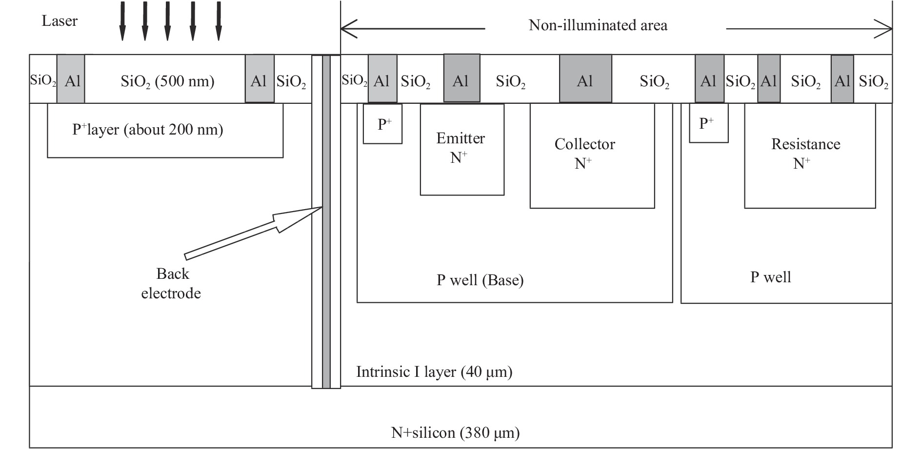
图6是PIN探测器和跨阻放大器两者集成的结构图。从结构上来看,图6左半部分是PIN探测器的光照区,右半部分是PIN探测器的非光照区。因为要利用非光照区的本征I层来制作跨阻放大电路中需要的NPN三极管和电阻,而不是在标准的P型衬底上,所以首先必须在本征I层上通过离子注入形成两个P阱与本征I层进行隔离,然后在两个P阱中分别制作NPN三极管和电阻。考虑到横向NPN三极管的结构相比于纵向NPN三极管简单,工艺上较容易实现,所以采用了横向NPN三极管的结构。电阻是通过在P阱(电阻区)进行一次离子注入形成的,电阻两端由Al电极引出。可以看到PIN探测器的结构相比于图4中的结构并没有发生变化,只是将原来PIN探测器背面N+层的电极引到了上表面,与电路进行互连。

Figure 6. Process structure diagram of photoelectric monolithic integration
下面列举了光电单片集成的主要工艺步骤。
(1) PECVD法沉积SiO2,光刻并在本征I层上湿法腐蚀出对准标记。
(2) 重新沉积 SiO2作为离子注入掩蔽层,光刻出离子注入窗口,在本征层注入硼(B+)离子,形成横向NPN三极管的基区P阱和电阻区P阱,结深在900 nm左右。
(3) 高温退火,退火温度850 ℃,时间20 min。
(4) 重新沉积SiO2作为离子注入掩蔽层,光刻出离子注入窗口,在本征层注入磷(P+)离子,分别形成横向NPN三极管的集电极、发射极和电阻,结深在350 nm左右。
(5) 高温退火,退火温度800 ℃,时间20 min。
(6) 重新沉积SiO2作为离子注入掩蔽层,光刻出离子注入窗口,在本征层注入硼(B+)离子,分别形成两个阱区的欧姆接触和PIN探测器的P+层,结深200 nm左右。
(7) 高温退火,退火温度500 ℃,时间10 min。
(8) 重新沉积SiO2作为湿法腐蚀本征层的掩蔽层,光刻出刻蚀窗口,刻蚀出金属接触孔。
(9) 重新沉积500 nm厚的SiO2作为钝化减反膜,套刻形成金属电极互连。
从工艺上来看,整套光电单片集成工艺主要包括七次光刻、三次离子及三次高温退火。工艺的参数决定了器件的性能,为了保证PIN探测器在工艺参数不发生改变的情况下,实现和横向NPN三极管以及电阻的工艺兼容,必须将PIN探测器的关键工艺即离子注入形成P+层和接下来的高温退火放到最后一次离子注入和高温退火工艺中做。因为PIN探测器P+层离子注入后的退火为500 ℃,相比于横向NPN三极管的基区以及发射极和集电极的退火温度较低,而且时间较短,所以退火之后对横向NPN三极管以及电阻的工艺参数影响较小,相反如果先做PIN探测器P+层离子注入以及高温退火,接下来不管是横向NPN三极管的基区退火温度和时间还是发射极和集电极退火温度和时间都将会严重改变PIN探测器的工艺参数,影响其性能。所以在设计光电单片集成芯片的工艺流程时,并没有改变PIN探测器的工艺流程。
在光电单片集成设计中,从结构和工艺两方面都实现了PIN探测器和跨阻放大器两者的兼容,保证了PIN探测器的结构和性能没有发生改变。
-
如图7所示,测试得到了集成前流片成功的PIN探测器的I-V曲线、C-V曲线和光电响应曲线。图7(a)中PIN探测器的暗电流随反向偏压的增大而增大,当反偏在0~3 V之间时,反向暗电流大小在0~15 nA之间,暗电流很小。并且跨阻放大电路的输出端有隔直电容,如图4所示,所以暗电流对输出脉冲电压信号的影响可以忽略。

Figure 7. PIN detector performance test. (a) I-V curve; (b) C-V curve; (c) Photoelectric response curve
从图7(b) C-V曲线上可以看到在PIN探测器反偏电压达到4 V时,PIN探测器两端的结电容开始趋于稳定,大小为92 pF。
图7(c)是PIN探测器的光电响应曲线,是在恒定激光光源下测试的结果,所用红外激光波长是860 nm,分别测试不同光功率下PIN探测器直流光电流的大小,最后计算得到PIN探测器的响应度为0.6 A/W。
-
为了得到光电集成芯片输出的脉冲电压信号相对于集成前PIN探测器脉冲光电流信号的放大倍数,此次实验搭建了真实的测试系统,所用信号源为脉冲激光信号,波长为860 nm、脉冲宽度为100 ns、工作频率为10 kHz、信号源和目标的距离设置为5 m。为了排除外界噪声对测试结果的影响,整个测试过程在黑暗环境下进行,结果如图8所示。

Figure 8. Real pulse voltage response. (a) PIN detector; (b) Optoelectronic monolithic integrated chip
图8(a)是集成前PIN探测器探测到的脉冲光电流信号,可以看到脉冲光电流信号大小为1.85 μA左右,脉冲宽度为110 ns,对信号源脉宽仅展宽了10 ns。在相同的测试条件下对光电单片集成芯片的脉冲响应进行了测试,如图8(b)所示,可以看到脉冲电压信号的脉冲宽度基本没有发生变化,大小为1.85 mV左右,相比于PIN探测器的光电流信号1.85 μA放大了1000倍,即跨阻放大器的跨阻增益为1000,跨阻增益和跨阻阻值的理论值1000 Ω一致。
-
根据引信系统中激光接收模块的实际需要,提出了一种全新并且具有很强实用价值的光电单片集成的设计方法,即以PIN探测器器件为基础,在没有改变PIN探测器结构和性能的情况下,利用其非光照区的本征层面积集成了跨阻放大电路,并流片成功。最后测试得到跨阻放大器对PIN探测器脉冲光电流信号放大了1000倍,即与混合电路相比,在相同的探测距离下,通过将PIN探测器和跨阻放大器进行光电单片集成,使得PIN探测器上输出端信号的信噪比提高了三个数量级,从而可以提高激光接收模块的抗干扰能力,同时也可以减少系统面积。
基于现有的数据和经验,一方面可以通过沟槽工艺将PIN探测器的光照区和非光照区进行隔离来进一步减少其暗电流;另一方面可以设计多级放大电路,通过多层金属布线的工艺将整个放大电路都集成到PIN探测器的非光照区上,实现激光接收模块中PIN探测器和整个放大电路的光电单片集成。
Photoelectric monolithic integration of PIN detector and transimpedance amplifier
doi: 10.3788/IRLA20210076
- Received Date: 2021-01-18
- Rev Recd Date: 2021-04-21
- Publish Date: 2021-09-23
-
Key words:
- photoelectric monolithic integration /
- PIN detector /
- horizontal NPN transistor /
- transimpedance amplifier
Abstract: A silicon-based PIN detector was designed, which had large area and high response, the surface area of the PIN detector was 4.1 mm×13.8 mm, and the thickness was about 420 μm. The ring-shaped Al electrode was used to extract the photocurrent signal in the photosensitive surface of the PIN detector. The test was performed under a constant laser light source with a wavelength of 860 nm, and its responsivitywas 0.6 A/W. Next, a new feasibility method for photoelectric monolithic integration was proposed, that is, by using the intrinsic I layer area of the non-illuminated area of the PIN detector, a transimpedance amplifier compatible with the structure and process of the PIN detector was designed, the photoelectric monolithic integration of the PIN detector and the transimpedance amplifier was realized on the premise that the structure and performance of the PIN detector had not changed. Finally, under the actual pulsed laser signal with a wavelength of 860 nm, a pulse width of 100 ns, and a working frequency of 10 kHz, the pulse response of the successful tape-out PIN detector and the photoelectric monolithic integrated chip was compared and tested. The results show that the pulse voltage signal of the photoelectric monolithic integrated chip is amplified by 1000 times compared with the pulse photocurrent signal of the PIN detector, while the pulse width is basically unchanged, the amplification factor is consistent with the theoretical transimpedance value of 1000 Ω. The integrated photoelectric chip is used in the laser receiving module of the laser fuze system. Through photoelectric monolithic integration, the signal-to-noise ratio of the output signal on the PIN detector can be improved, and the stability of the system can be enhanced, it can also meet the needs of the miniaturization of the laser fuze system.


 DownLoad: