


-
红外焦平面阵列探测器(Infrared Focal Plane Arrays Detector,IRFPAs)具有灵敏度高、环境适应性好、抗干扰能力强、质量轻、功耗低等优点,被广泛应用于航空航天、红外遥感、国防、气象、环境、医学及通信领域[1-4]。在中波红外探测领域,锑化铟(InSb)IRFPAs因具有材料均匀性好、时间稳定度高的优点,备受科研人员的关注。批量生产中,液氮冲击下InSb IRFPAs经常出现的局部分层、局部碎裂等失效现象已成为制约其成品率提升的瓶颈,因此探究InSb IRFPAs局部分层失效机理成为目前迫切需要解决的问题。
针对InSb IRFPAs的局部分层失效问题,贵磊等[5-6]在局部分层易发生区域添加内聚力单元,基于张开型内聚力模型对局部分层进行分析,认为界面法向应力是引起局部分层的主要原因;孟庆端等[7]以面内剪切应力分布为判据,认为局部分层源于面内剪切应力。这些研究能够部分解释局部分层失效现象,但仅在易分层处添加内聚力单元的做法,人为的因素过重,缺乏合理性及普适性;仅考虑面内剪切应力而忽略面外法向应力的做法也有失偏颇。为了更全面、更深入剖析局部分层失效诱因,文中拟采用在InSb芯片与底充胶的界面处铺满内聚力单元,同时考虑界面法向应力,通过改变张开型和滑开型裂纹扩展模式的比例,系统分析局部分层分布特征随裂纹扩展混合比例的演化规律,对比实测局部分层分布特征,定量给出器件局部分层失效诱因和失效机理。
-
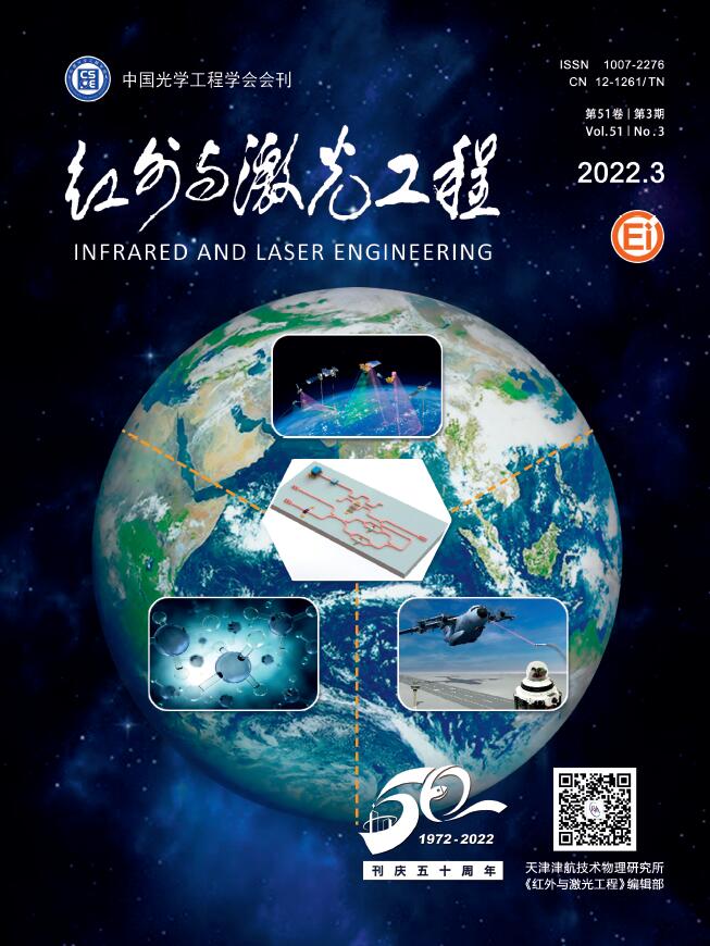
在线弹性断裂力学中,根据驱动力与裂纹扩展之间的内在关系可将裂纹划分为张开型裂纹、滑开型裂纹和撕开型裂纹,如图1所示。其中张开型裂纹扩展的特征为:拉应力垂直于裂纹面,裂纹扩展方向和拉应力垂直;滑开型裂纹扩展的特征为:剪应力位于裂纹面内,并与裂纹扩展方向平行;撕开型裂纹扩展的特征为:剪应力位于裂纹面内,并与裂纹扩展方向垂直。在因热失配引起的层状结构局部失效中,不会出现撕开型裂纹扩展模式,因此在文中只考虑张开型和滑开型裂纹扩展模式。
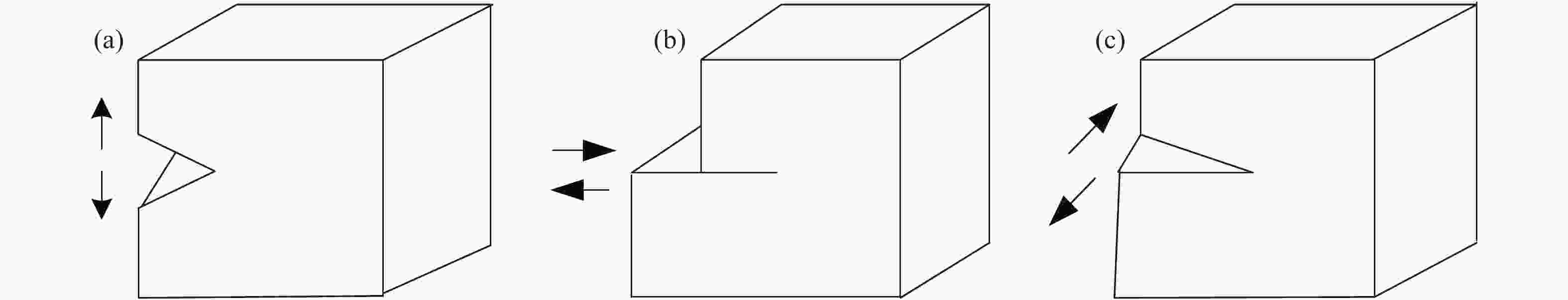
Figure 1. Schematic diagram of three typical crack expanding mode. (a) Mode I crack(opening mode); (b) Mode II crack(sliding mode); (c) Mode III crack(tearing type)
在描述裂纹的萌生与扩展时,以计算精度和成本为判据,通常认为双线性模型在众多本构关系模型中性能最佳,故文中采用由Aifanoh和Crisfield [8]建立的双线性牵引-分离内聚力模型。这里以张开型裂纹扩展为例介绍内聚力模型的参数设置,模型中运用的牵引-分离法则如图2所示:右下角的横坐标代表界面在法向拉应力作用下发生的分离量δ,纵坐标表示界面法向拉应力σ。当界面法向拉应力从0增加到σmax的过程中,界面之间的位移线性增加而不发生分层,法向拉应力一旦越过σmax,开始萌生界面局部分层,局部分层萌生后施加于界面上的法向拉应力则线性降低,当界面法向拉应力从σmax减小到0时,界面完全脱开,界面分层完成,此时对应的界面间距为δn。

Figure 2. Diagram of bilinear traction-separation rule of cohesive zone modeling
在双线性内聚力模型中,张开型模式下的σmax和δn与滑开型模式下的τmax和δt是内聚力模型设置的重要参数。文中着重研究InSb芯片和底充胶(Underfill)之间的界面脱粘开裂过程,故而内聚力模型中参数的设置由界面断裂能决定。Xu等[9]对复合材料结构粘接破坏的统一内聚力模型及其参数识别进行研究,实验测得双线性内聚力模型下界面断裂能为0.873 N/mm。周清春等[10]对衬底界面粘接力学特性进行研究,实验测得胶粘剂与衬底之间I型界面断裂能普遍在0.9 N/mm。Guo等[11]通过实验测得胶粘剂与粘接界面之间I型和II型断裂能分别为0.3 N/mm和0.6 N/mm。Bellali等[12]通过内聚力模型和有限元分析法预测复合材料对铝缺口增强板损伤的补偿特性,测得用胶粘剂AV138粘接界面时的I型和II型断裂能分别为0.2 N/mm和0.38 N/mm。在上述粘接结构脱粘开裂的研究中,I型和II型断裂能值普遍分布在0.1~1 N/mm,故而笔者选取Underfill与InSb芯片脱粘时I型和II型断裂能应介于0.1~1 N/mm之间。在研究胶粘剂与衬底之间的分层实验中,测得的分层位移大多在毫米量级,故此文中选取1 mm作为Underfill与InSb芯片脱粘时的临界位移分离量。
考虑到器件局部分层主要发生在界面处,张开型和滑开型裂纹扩展混合模态比可从纯滑开型(0: 10)演变到纯张开型(10: 0)。当张开型和滑开型混合模态比设置为4: 6时,模拟结果与实测结果高度吻合。此时设置的张开型与滑开型界面断裂能分别为0.292 N/mm和0.441 N/mm,对应的法向粘接力和切向粘接力分别为882.6 kPa和583.5 kPa。笔者注意到Chen等[13]在研究Underfill材料对倒装焊结构可靠性影响时,测得的Underfill与芯片之间的界面粘接强度普遍介于122~851 kPa之间,这间接证实了文中参数选取的合理性。内聚力参数的选取如表1所示。
Mixed-mode
ratios, ωNormal cohesive traction Normal displacement jump Tangential cohesive traction Tangential displacement jump σ0/kPa δI0/mm τ0/kPa δII0/mm 9∶1 116.7 1 1050 1 8∶2 257.2 1 1029 1 7∶3 414 1 975 1 6∶4 583.5 1 882.6 1 5∶5 750 1 750 1 4∶6 882.6 1 583.5 1 3∶7 975 1 414 1 2∶8 1029 1 257.2 1 1∶9 1050 1 116.7 1 Table 1. Parameter setting of cohesive zone modeling under different mixed-mode ratios
-
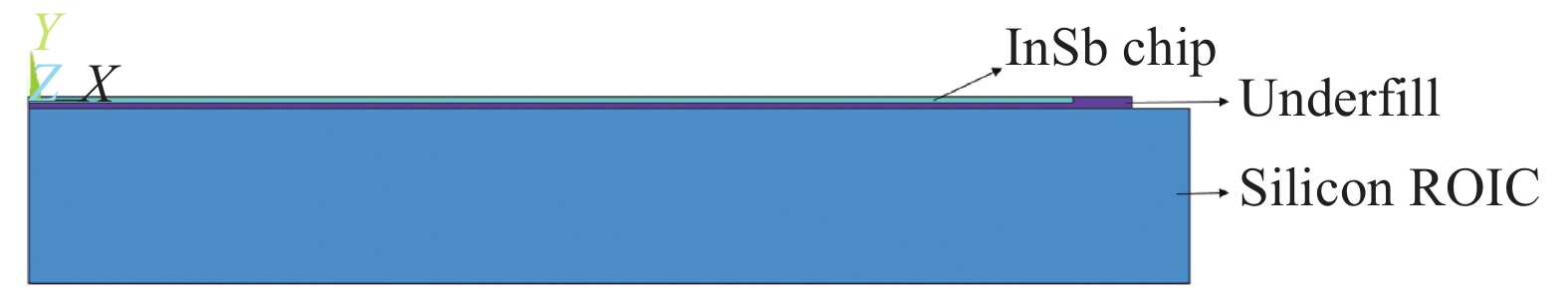
InSb IRFPAs通常由三层材料堆叠而成,采用倒装技术将最上面的InSb光敏元芯片与最下面的Silicon ROIC(Readout Integrated Circuits)通过铟柱阵列进行互连,铟柱阵列和Underfill相间排列构成中间层,这里Underfill呈网状结构环绕着铟柱阵列。在铟柱阵列和Underfill的相间排列区域,铟柱阵列的体积通常不超过整个中间层体积的16%,在局部分层易发生区域,铟柱更少。为便于分析,文中暂且忽略铟柱对局部分层的影响。考虑到InSb IRFPAs结构的对称性,选取整个探测器结构的1/2进行建模。在建立的模型[14-15]中,InSb芯片、Underfill、和Silicon ROIC的厚度分别为10 µm,10 µm和300 µm,其中Underfill边缘部分的厚度为20 µm,呈fillet结构包围着InSb芯片,这源于器件加工过程中的底充胶填充固化后,通常包围着InSb芯片的缘故。模型中InSb芯片、固化后的Underfill和Silicon ROIC都视为线弹性材料,其具体材料参数如表2所示。网格单元采用PLANE182,在InSb芯片与Underfill的界面处全部覆盖上接触单元CONTA172,目标单元选用TARGE169,接触算法设置为增强拉格朗日算法,接触模式为Bonded(多数),用于实现界面分层。二维结构模型示意如图3所示。
Materials Elastic modulus, E/GPa Poison’s ratio, μ Temperatures, T/K InSb chip 409(in plane)
123(out of plane)0.35 77–300 Underfill 0.0002/α 0.30 77–300 Silicon ROIC 163 0.28 77–300 $\alpha = 22.46 \times {10^{ - 6}} + 5.04 \times {10^{ - 8}} \times {\rm{(}}T{\rm{ - }}273{\rm{)}}$, K是开式温度单位 Table 2. Related material parameters of InSb IRFPAs

Figure 3. Two-dimensional finite element model for InSb IRFPAs
-
历经液氮冲击后,模拟得到的探测器的位移分布见图4中的左上半部分所示。显然,在InSb芯片与Underfill的界面处出现了局部分层,局部分层临近器件边缘区域。为明晰局部分层的演化过程,提取了300 K、200 K、100 K和77 K时模拟得到局部分层分布结果,如图4的右半部分所示。在液氮冲击前,对应的温度为300 K,InSb芯片与Underfill粘合在一起;伴随着器件温度的不断降低,局部分层开始萌生并不断扩展,当温度T=200 K时,InSb芯片与Underfill之间沿法线方向呈分离状态,面间最大分离距离为0.04 μm,界面分层涵盖的归一化坐标范围为0.872~0.944;当温度T=100 K时,InSb芯片沿法向方向高高隆起,局部分层呈现出进一步向两侧扩展的态势,面间最大分离距离为0.08 μm,界面分层涵盖的归一化坐标范围为0.855~0.933;当温度降到77 K时,InSb芯片与Underfill之间局部分层更加明显。在整个降温过程中,Underfill上表面始终保持在相对平整的状态。
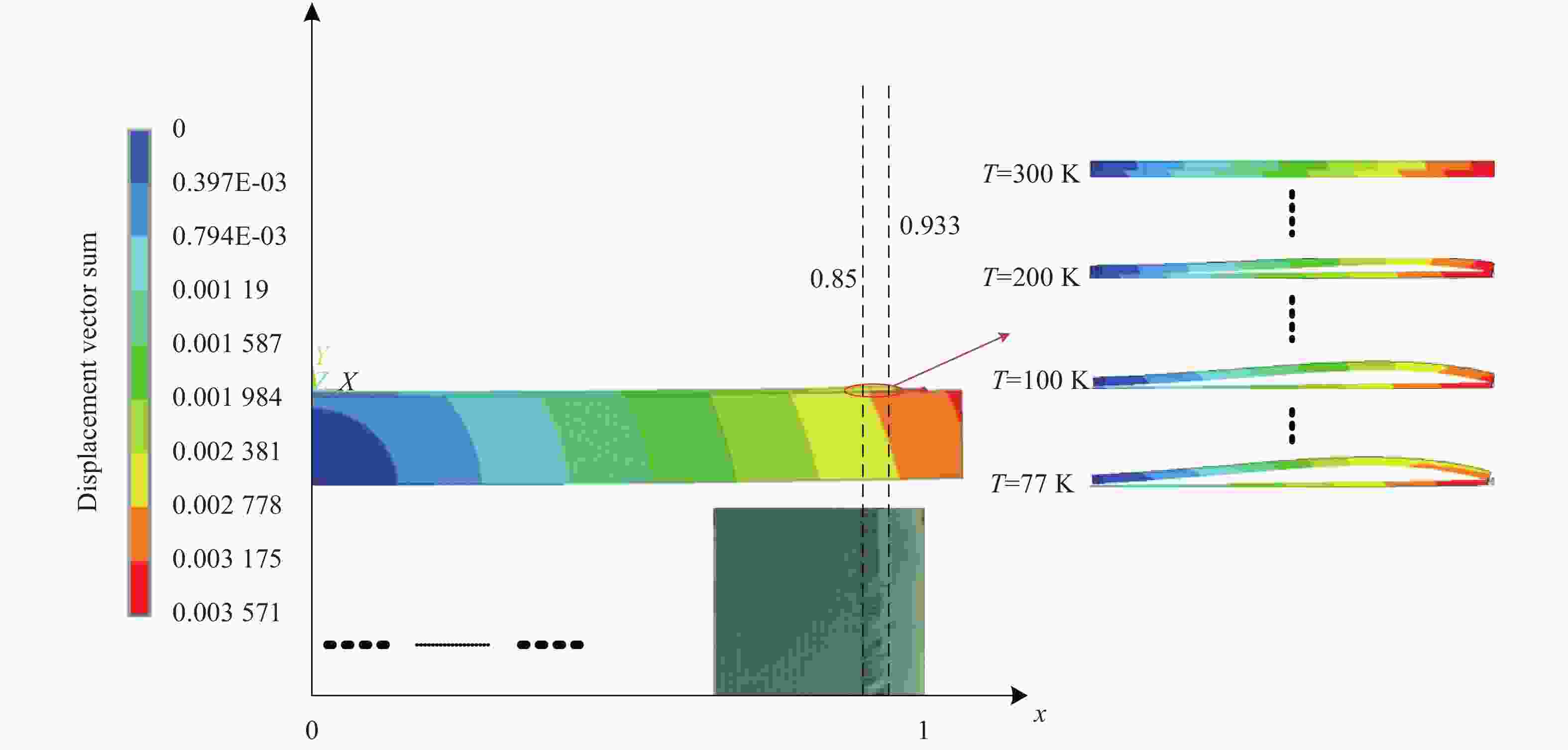
Figure 4. Simulated results for displacement vector sum vs. the measured photograph of InSb IRFPAs detector after the liquid nitrogen shock
为明确IRFPAs局部分层失效机理,笔者将InSb IRFPAs分层模拟结果与实测局部分层照片分别进行归一化处理,见图4的左下半部分。对于实测局部分层照片,以铟柱位置为参考,结合器件加工光刻版图,认为实测局部分层涵盖范围对应于从器件中心点起始的第64个铟柱至第68个铟柱之间的区间,归一化坐标区间为0.853 ~ 0.933。对于模拟结果而言,局部分层范围的确认是以发生局部分层的节点进行判断的,归一化坐标区间为0.85 ~ 0.933。显然,模拟结果与典型实测局部分层涵盖范围基本一致,证实了InSb IRFPAs局部分层应该属于张开型和滑开型共生的混合型局部分层失效的设想。
-
工程实际中界面分层通常既包含张开型裂纹扩展模式,也包含滑开型裂纹扩展模式。在这两种模式共同作用下,界面断裂能量G是张开型裂纹扩展断裂能Gn和滑开型裂纹扩展断裂能Gt的和,其中Gn和Gt分别用下式描述:
对于混合型分层模式,法向应力和切向应力均对界面断裂能量
$G$ 有贡献,在Gn和Gt分别达到各自的临界断裂能Gcn和Gct之前就可以实现界面分层,这可采用基于幂次律的能量准则[16]来定义局部分层过程:其中
由公式(1)~(4)可知,混合模态在张开型和滑开型裂纹扩展模式之间以椭圆形式平稳地变化,由此可得张开型和滑开型裂纹之间的扩展权重,即混合模态比ω可定义如下:
式中:σ0、τ0分别为混合模态下系统达到界面分层时的法向粘接力和切向粘接力;δI0、δII0分别为混合模态下系统达到界面分层时的法向位移分离量和切向位移分离量。
为了更全面地剖析局部分层诱因,明晰张开型和滑开型裂纹扩展权重对InSb IRFPAs局部分层分布特征的影响,笔者在内聚力模型中调整混合模态比例,系统研究张开型与滑开型裂纹扩展权重的比例取不同值时,局部分层涵盖范围的变化规律。
混合模态比取不同值时局部分层涵盖范围的模拟结果如图5所示。当张开型和滑开型裂纹扩展权重比从9: 1依次调整到4: 6的过程中,局部分层的左边缘坐标由0.733逐渐增加到0.85,局部分层的右边缘坐标从0.872逐渐增加到0.933;当混合模态比越过4: 6时,局部分层左边缘坐标由0.85逐渐降低并趋于稳定到0.839,局部分层右边缘坐标则一直稳定在0.933附近。

Figure 5. Local delamination position under different mixed-mode ratios
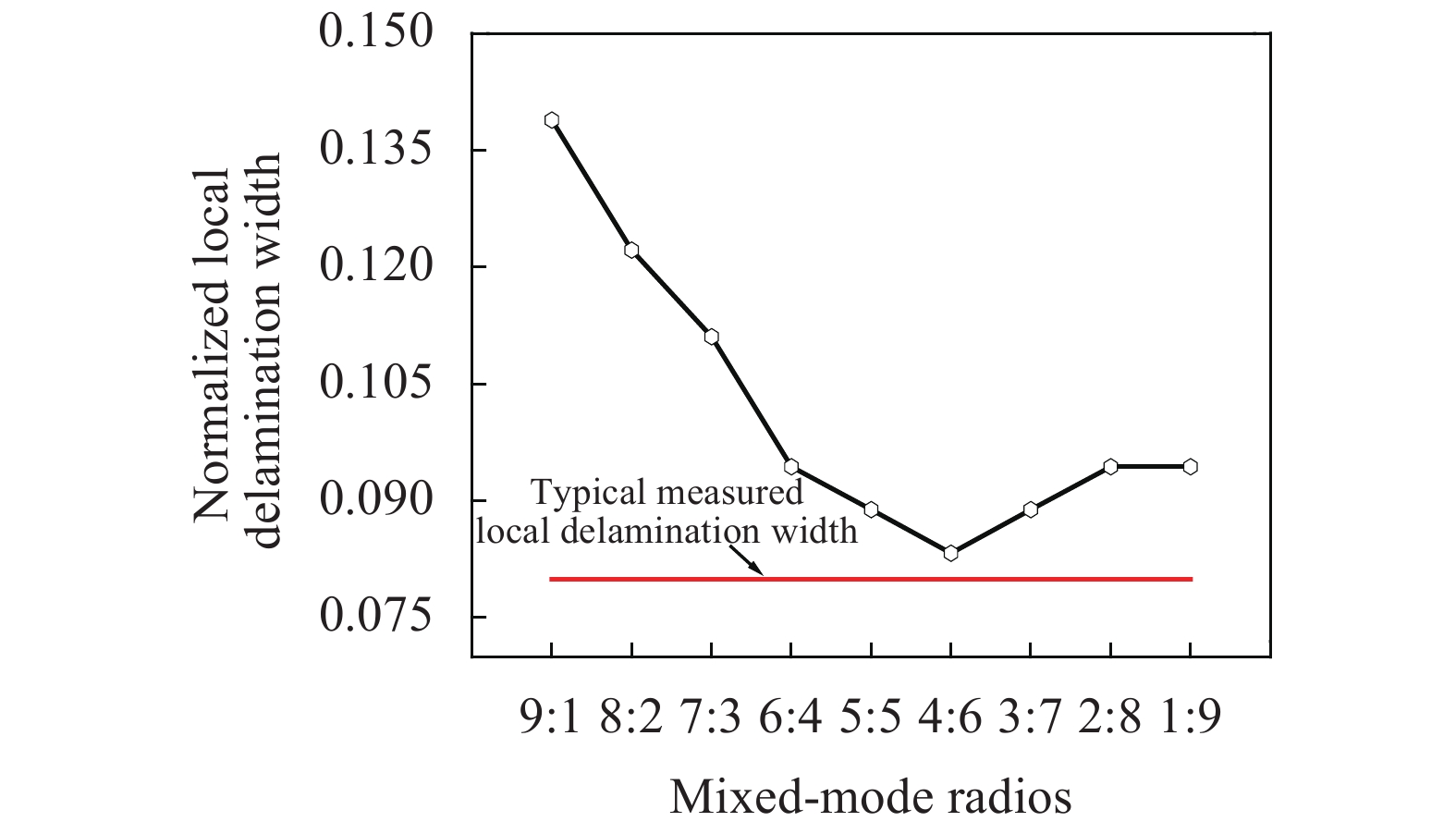
为便于比对,笔者提取了局部分层涵盖范围随混合模态比的演化趋势,如图6所示。当张开型和滑开型裂纹扩展权重比从9∶1依次调整到4∶6时,模拟得到的局部分层归一化坐标宽度近似线性减小;扩展权重比一旦越过4∶6,局部分层归一化坐标宽度则线性增加,最后稳定在0.094附近。当裂纹扩展权重比取4∶6时,模拟得到的局部分层宽度和归一化坐标涵盖位置最接近实测照片中的局部分层宽度和分层位置,由此笔者断定InSb IRFPAs局部分层混合失效模式中张开型和滑开型裂纹扩展的权重比为4∶6,其中滑开型裂纹扩展模式占主导,这与Xiao[17]所做的结论基本一致,这进一步证实了文中所得结论的正确性。

Figure 6. Local delamination occupying width under different mixed-mode ratios
-
为了明晰InSb IRFPAs局部分层的失效诱因和机理,采用混合型内聚力模型,在接触面铺满内聚力单元,建立二维结构模型进行分析。认为当张开型和滑开型裂纹扩展的权重为4: 6时,模拟得到的局部分层宽度和局部分层归一化坐标位置与典型实测局部分层照片完全一致,表明InSb IRFPAs的局部分层源于界面法向应力和面内剪切应力共同作用,属于典型的混合型局部分层模式,并且滑开型局部分层模式占主导。
Research on local delamination failure mechanism of InSb infrared focal plane arrays detector
doi: 10.3788/IRLA20210133
- Received Date: 2021-03-04
- Rev Recd Date: 2021-05-14
- Publish Date: 2022-04-07
Fund Project:
Young Scientists Fund of the National Natural Science Foundation of China (Grant No. 61505048);the Key Scientifc Research Projects of Higher Education Institutions in Henan Province (Grant No. 19A510012); Natural Science Foundation of Henan Province(202300410157)
-
Key words:
- InSb IRFPAs /
- cohesive zone model(CZM) /
- local delamination /
- mixed-mode ratios
Abstract: Local delamination failure phenomena of indium antimonide infrared focal plane detectors (InSb IRFPAs) in their mass production have become a bottleneck restricting the improvement of their final yield. In order to determine the inducement of local delamination in InSb IRFPAs, the interface between the InSb chip and the underlying underfill with cohesion units was covered, and the specified parameters in cohesion model were optimized, finally the two-dimensional model of local delamination failure analysis of InSb IRFPAs was established. Simulation results are verified by the measured distribution characteristics of local delaminations, that is, (1) Most local delamination appears in the surrounding edges of InSb chip, and occupies a certain width; (2) Once the InSb chip is separated from the underlying underfill in the normal direction, the local delamination will expand gradually toward its both sides of the plane. In order to clarify the inducement of the local delamination, the evolution rule of the local delamination with different mixed-mode ratios is systematically analyzed under the jointed action of both the opening mode and sliding mode. The simulation results are highly consistent with the measured results when the mixed-mode ratio between the opening mode and the sliding mode is set to 4: 6. The local delamination of the InSb IRFPAs are ascribed to the jointed action of both the interfacial normal stress and the in-plane shear stress, is the typical mixed-mode local delamination mode, furthermore, the sliding local delamination mode is dominant.


 DownLoad: