


-
量子通信是利用量子叠加态和纠缠效应进行信息传递的新型通信方式,基于量子力学中的不确定性、测量坍缩和不可克隆三大原理提供无法窃听和计算破解的绝对安全性保证,主要分为量子隐形传态和量子密钥分发两种。量子隐形传态目前处于理论和实验探索阶段,离实用尚有很大差距;量子密钥分发,借量子叠加态的传输测量实现通信双方安全的量子密钥共享,采用一次一密的对称加密体制,即通信双方均使用与明文等长的密码进行逐比特的加解密操作,实现无条件的绝对安全的保密通信,分光膜是量子密钥分发系统中一种重要光学元件。当光倾斜入射到普通分光膜元件时,将会产生S偏振光和P偏振光分离,入射角度越大,分离量越大,产生的偏振效应越强,同时也会产生严重的位相差,将影响量子密钥分发系统的性能,造成严重的误码率[1],因此,需要通过光学薄膜元件偏振和位相调控技术进行抑制,研制能够满足位相和偏振要求的分光膜元件,对整个系统意义重大。国内外在偏振和位相调控技方面展开了相关研究,V R Costich 通过不同折射率匹配设计消偏振的分束器[2],顾培夫等人利用宽带F-P消偏振特性,设计长/短波通截至滤光片[3],马小风等人设计偏振效应可调的减反射膜[4],但是针对文中研究的宽波段特殊分光比的消偏振位相调控膜没有找到相应的文献报道,具有一定研究价值。
-
基于空间量子通信的技术要求进行分光膜系的设计,允许有一定的吸收,具体技术要求如表1所示。
Average T:R@1500-1600 nm (8±2)∶(92$ \mp 2 $) $\left|{{T} }_{s}-{{T} }_{p}\right|$ and $\left|{{R} }_{s}-{{R} }_{p}\right|$ ≤3% $ \left|{\Delta }_{t}\right| $@1530 nm, 1540 nm, 1550 nm, 1560 nm ≤7° $ \left|{\Delta }_{r}\right| $@1530 nm, 1540 nm, 1550 nm, 1560 nm ≤10° Table 1. Technical requirements of beam splitter
-
文中采用对称膜系的等效层设计理念[5-6],以膜系(qpq)为例,来解释对称膜系在数学上存在等效层的概念。对称膜系特征矩阵为:
式中:M表示特征矩阵符号;
$ {\mathrm{\delta }}_{\mathrm{q}} $ 表示q层的位相厚度;$ {\mathrm{\delta }}_{\mathrm{p}} $ 表示p层的位相厚度;$ {\mathrm{\eta }}_{\mathrm{q}} $ 表示q层的有效导纳;$ {\mathrm{\eta }}_{\mathrm{p}} $ 表示p层的有效导纳。由于对称膜系的特征矩阵和单层膜的特征矩阵具有相同的性质,可表示为:
式中:E为等效折射率;
${\varGamma }$ 为等效位相厚度。因此,对称膜系(qpq)可以用等效单层膜来描述,该等效层的等效折射率E和等效位相厚度
${\varGamma }$ 可以由以下公式确定: -
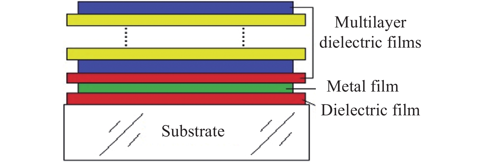
分光膜系设计的基本原则是在确定的衬底材料表面,使用最少的膜层,实现分光比要求,同时满足薄膜材料与衬底之间及薄膜材料之间的应力匹配,保证薄膜元件的可靠性。根据表1所示的分光膜技术要求,采用“介质+金属+多层介质膜”的复合结构,其示意图如图1所示,实现宽光谱能量的分光及位相调控。根据以上原则,偏振和位相调控分光膜的设计方法如下:(1)考虑薄膜材料的透明区、折射率、吸收系数及应力匹配,选择4种不同折射率的薄膜材料,其中J代表金属材料,H、M及L分别代表高、中、低折射率介质薄膜材料;(2)在薄膜材料确定的情况下,改变层数和厚度,可以得到不同等效位相
${\varGamma }$ 和等效折射率E,故可以采用MJM和HLH这样的对称膜系结构,初始膜系结构为:G|MJM HLH|AIR,其中G代表衬底,AIR代表空气。为满足1500~1600 nm波段光谱要求及偏振和位相的调控,可在初始膜系结构最外层增加L有利于优化设计,此时初始膜系结构变为:G|MJM HLHL|AIR。(3)设定优化目标。采用Simplex和Quasi Newton等多种优化方式,对各层薄膜厚度反复优化迭代,得到最终的优化结果。采用该方法可以在常见的光学玻璃材料上,获得较好的分光膜优化结果。
Figure 1. Structure diagram of beam splitter structure
金(Au)、银(Ag)、铝(Al)等是薄膜制备常采用的金属材料,其中Ag膜是已知金属材料中偏振效应最小[7-8],可优先选择。对于介质薄膜材料的选择,需要充分考虑光学特性,应力匹配等因素,选择SiO2、Al2O3、和Ta2O5三种介质薄膜材料[9-12],用于分光膜偏振和位相的调控。基于以上设计方法和镀膜材料选择,采用Essential Macleod膜系设计软件,参考波长1700 nm,入射角度45°,对基础膜系进行优化,优化结果为G|0.37444 M0.00438 J0.04772 M 0.07484 H0.19293 L0.22524 H0.25465 L|AIR,M代表Al2O3,J代表Ag ,H代表Ta2O5,L代表SiO2,理论设计光谱透过率曲线如图2所示,光谱反射率曲线如图3所示,透射位相如图4所示,反射位相如图5所示。
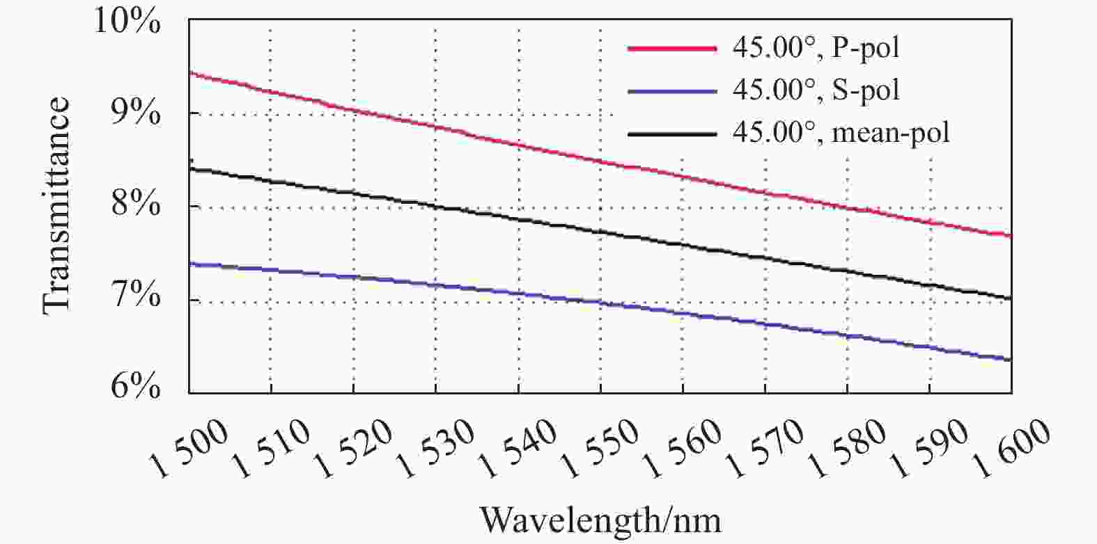
Figure 2. Spectral transmittance curve
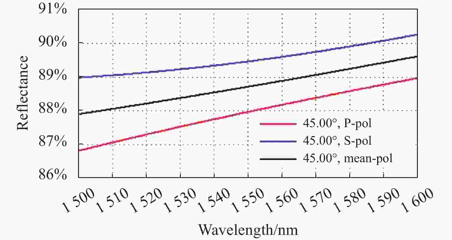
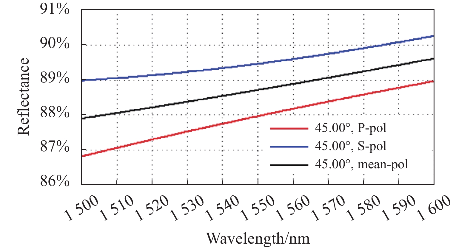
Figure 3. Spectral reflectance curve
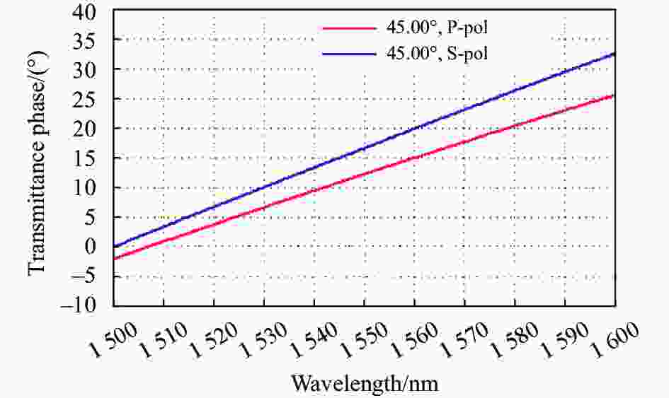
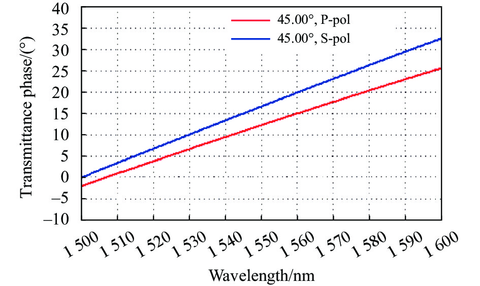
Figure 4. Transmission phase

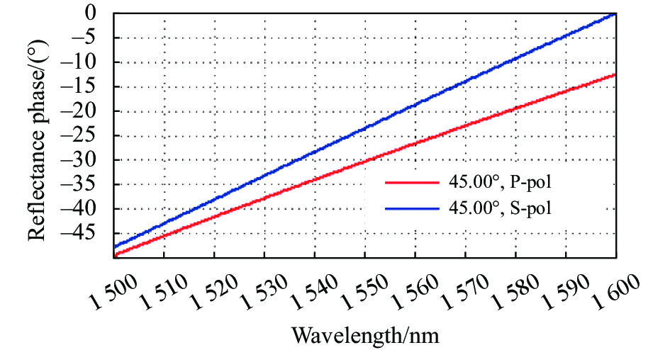
Figure 5. Reflection phase
由图2和图3可知,在1500~1600 nm平均T:R为8.5:91.5,P光平均透过率8.53%,S光平均透过率6.94%,P和S透过光谱在1500 nm处存在最大分离量2.04%;P光平均反射率87.93%,S光平均反射率89.51%,P和S反射光谱在1500 nm处存在最大分离量2.16%。由图4和图5可知,在1530、1540、1550、1560 nm处,P光和S光透过位相差分别为3.4°、3.9°、4.4°和4.9°,P光和S光反射位相差分别为4.6°、5.7°、6.8°和7.9°,满足分光膜的技术要求。
-
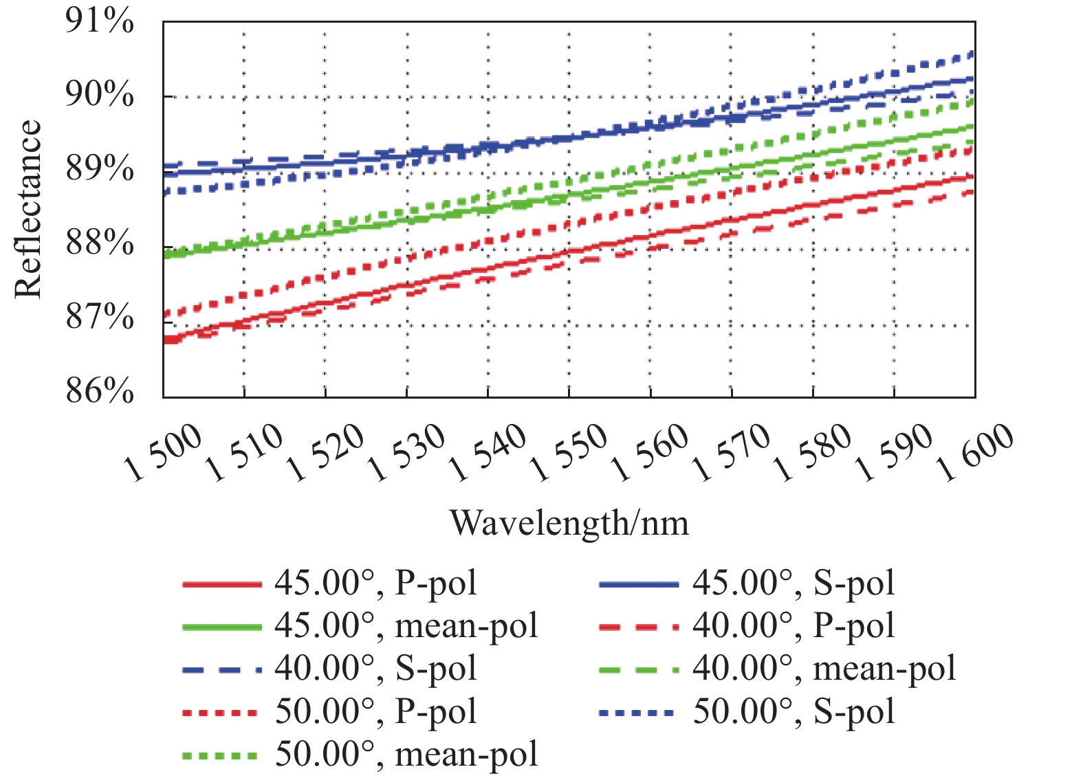
图6和图7分别给出40°、45°与50°入射时,S光、P光和平均光谱透过率曲线和光谱反射率曲线。

Figure 6. Spectral transmittance curve of differnt incident angles
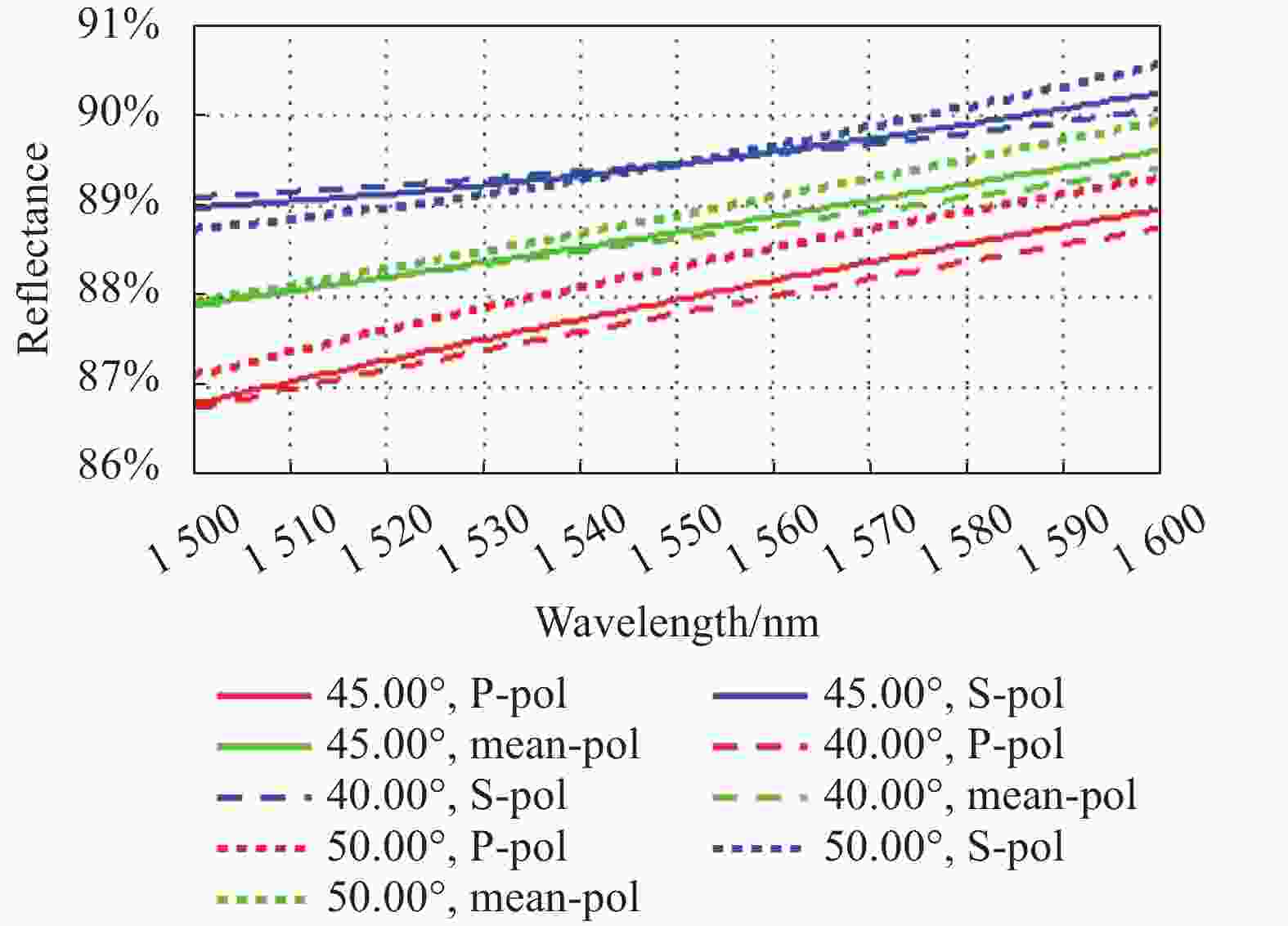
Figure 7. Spectral reflectance curve of differnt incident angles
由图6和图7可以看出,40°入射时,在1500~1600 nm平均T:R为8.06:91.94,P光平均透过率8.57%,S光平均透过率6.97%,P和S透过光谱在1500 nm处存在最大分离量2.06%;P光平均反射率87.73%,S光平均反射率89.51%,P和S反射光谱在1500 nm处存在最大分离量2.33%;50°入射时,在1500~1600 nm平均T:R为7.89:92.11,P光平均透过率8.34%,S光平均透过率6.90%,P和S透过光谱在1500 nm处存在最大分离量1.76%;P光平均反射率88.29%,S光平均反射率89.55%,P和S反射光谱在1500 nm处存在最大分离量1.67%。与45°入射时相比,透/反射比及S-P光最大分离量变化都较小。因此,该膜系结构对入射角度的变化不敏感,适合大角度变化的膜系设计。
-
分光膜的制备在LeyBold ARES1350 型真空镀膜设备上完成,Ag、SiO2、Al2O3和Ta2O5均采用电子束蒸发离子辅助沉积方式(APSpro源),由石英晶体控制膜层的沉积速率和厚度,制备工艺参数如表2所示。
Material Rate/nm·s−1 EB oxygenation/sccm APS Bias voltage/V Discharged current/A Al2O3 0.3 0 100 45 Ag 1 0 30 20 Ta2O5 0.3 35 130 50 SiO2 0.8 10 160 55 Table 2. Preparation process parameters
镀膜前,先对样片进行超声波清洗,然后采用酒精、乙醚混合液擦拭脱水后放入真空室。烘烤温度80 ℃,工件架转速20 rad/min,当真空度抽至1.0 ×10−5 mbar时,打开APS源对样片表面进行镀前离子束清洗200 s,目的是清洗样片表面,并在表面形成伪扩散层,有利于提高衬底与膜层之间的结合力。镀膜过程APS源充入氩气,gas1和gas2分别为4 sccm和10 sccm,当真空度到8.5 ×10⁻⁶ mbar时,开始薄膜沉积。
-
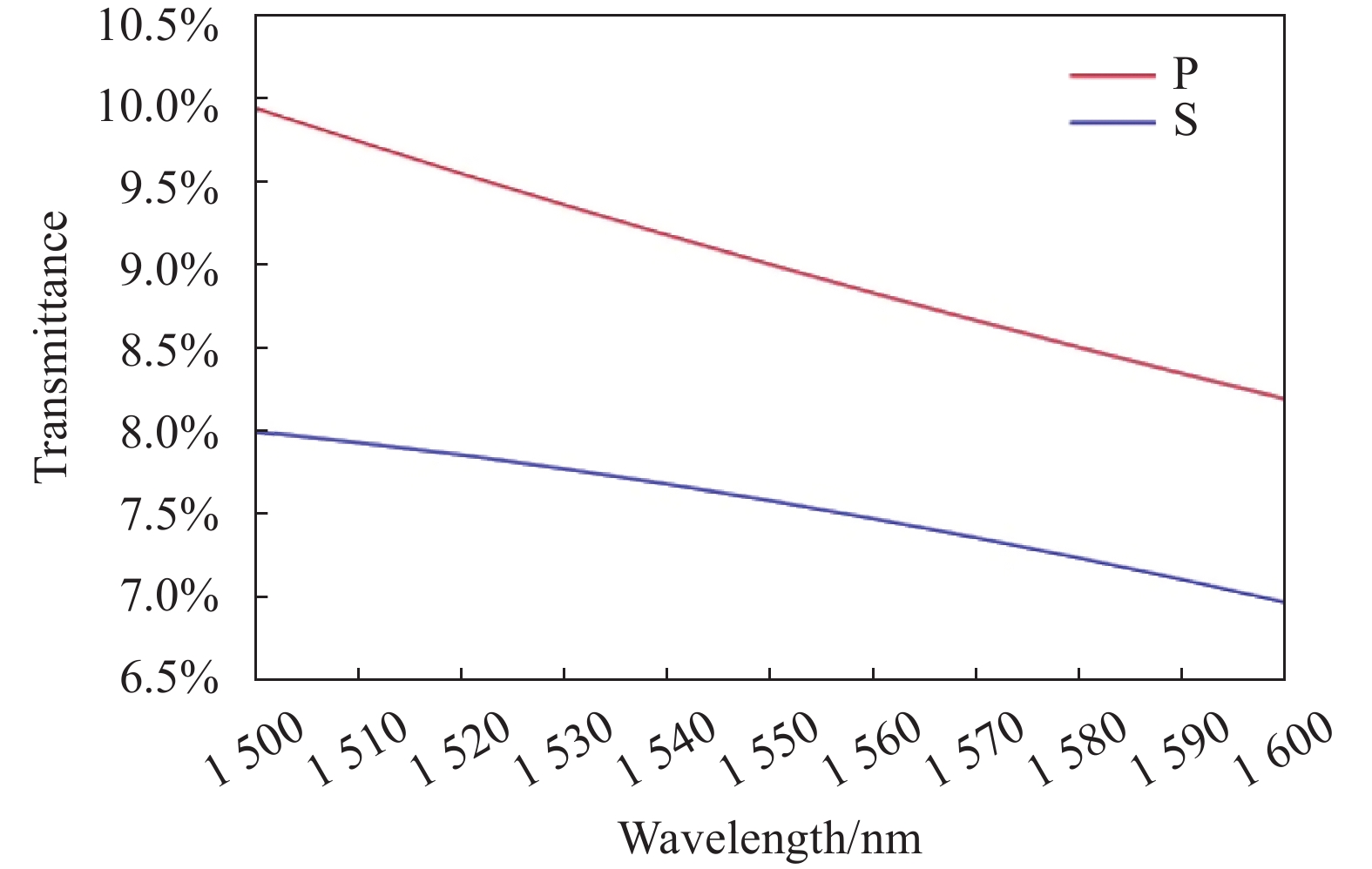
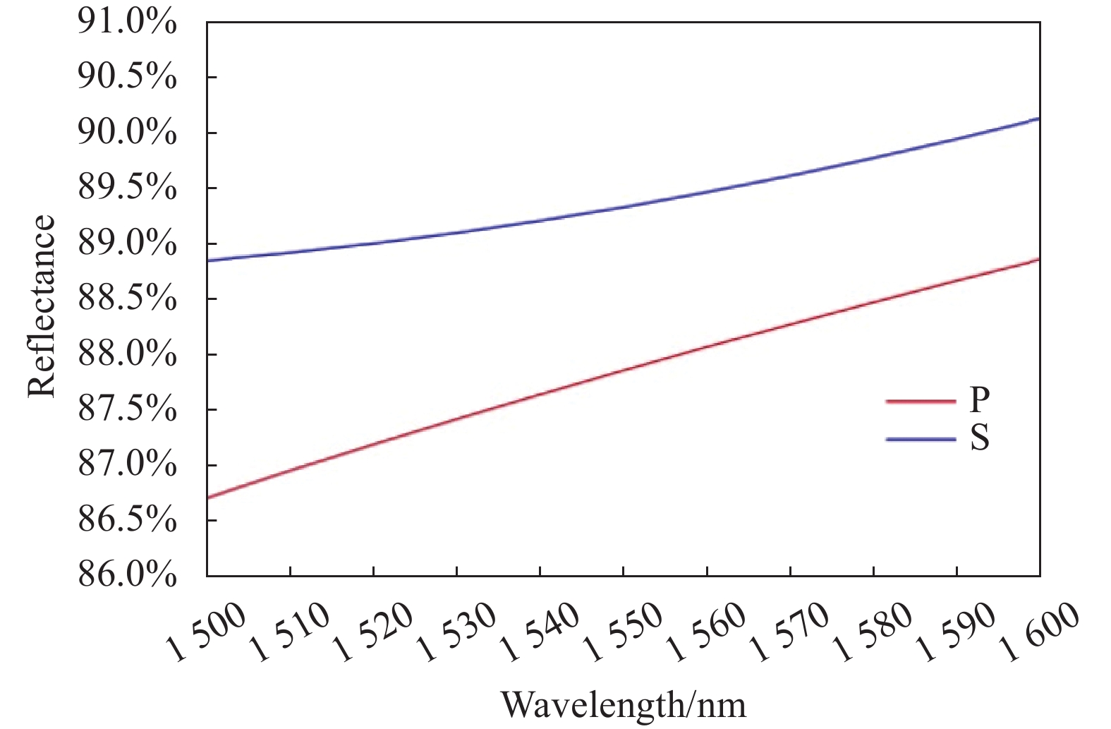
实际制备的样品如图8所示,采用Carry7000测得光谱透过率曲线如图9所示,光谱反射率曲线如图10所示。

Figure 8. Sample picture
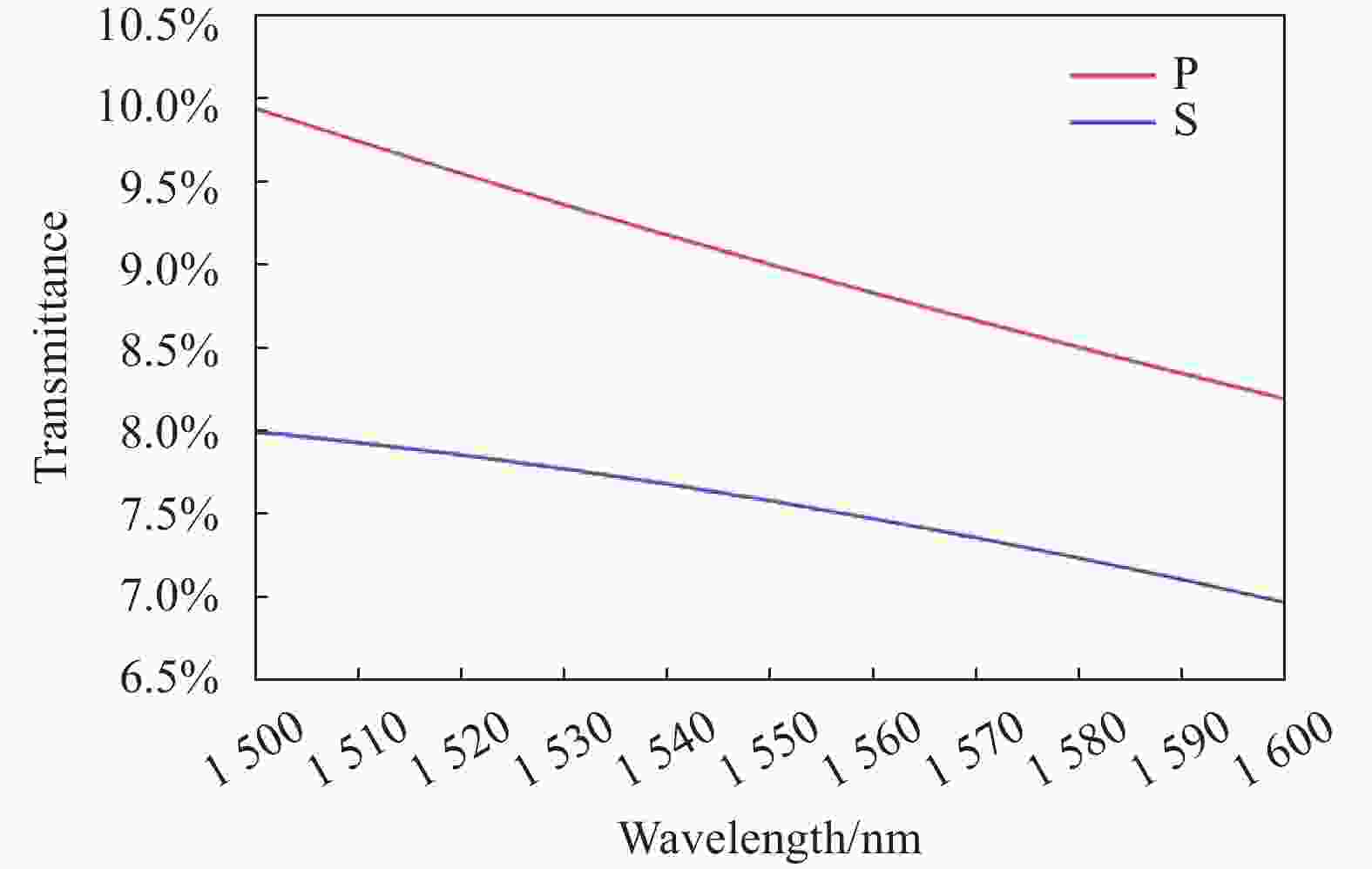
Figure 9. Measured spectral transmittance curve
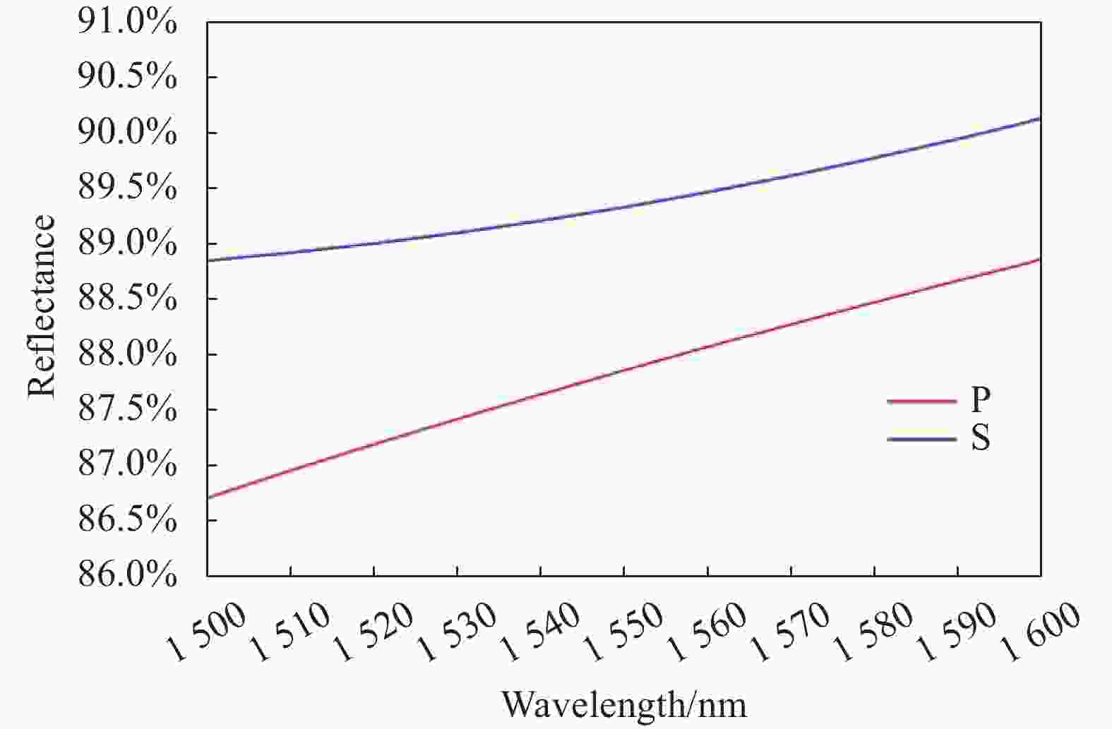
Figure 10. Measured spectral reflectance curve
由图9和图10可知,在1500~1600 nm波段,P光平均透过率9.01%,S光平均透过率7.52%,P和S透过光谱在1500 nm处存在最大分离量1.94%,P光平均反射率87.81%,S光平均反射率89.41%,P和S反射光谱在1500 nm处存在最大分离量2.14%,平均T:R为8.53:91.47。
-
通过光的电磁场理论,可以推导出S、P偏振光所引起的位相差
$ \mathrm{\delta } $ 与椭圆偏振光消光比(ER)的关系为[13]:由公式(5)可知,测得偏振消光比即可获得S、P偏振光所引起的位相差。文中采用旋转检偏器直接测量的方法,测得透射光/反射光的消光比。测量原理示意图如图11所示。
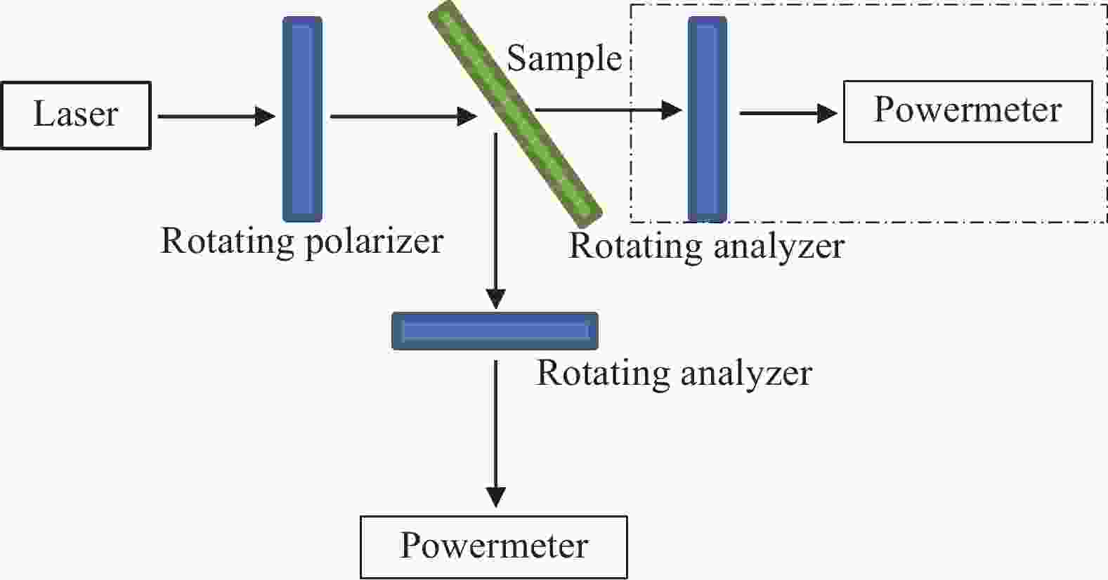
Figure 11. Schematic diagram of extinction ratio measurement principle
如图11所示,测量时分别采用1530、1540、1550、1560 nm激光器作为输入光源,激光束经过旋转起偏器后,以45°角入射在样品表面,经由样品表面透射(或反射),再通过旋转检偏器,最后由功率计接收。当入射光主偏正分量与检偏器主轴重合时,功率计获得最大功率(Imax);当入射光主偏正分量与检偏器主轴垂直时,功率计获得最小功率(Imin),样品的消光比可以通过公式(6)计算得出:
实测得到的消光比数据和结合公式(5)计算获得位相差如表3所示。
λ/nm Imax/mW Imin/mW ER $ \mathrm{\delta } $/(°) T R T R T R T R 1 530 0.43 4.24 0.402×10⁻³ 7.323×10⁻³ 1 070:1 579:1 3.5 4.76 1 540 0.41 4.31 0.502×10⁻³ 11.402×10⁻³ 817:1 378:1 4.01 5.89 1 550 0.40 4.37 0.593×10⁻³ 16.125×10⁻³ 675:1 271:1 4.41 6.95 1 560 0.38 4.43 0.731×10⁻³ 21.931×10⁻³ 520:1 202:1 5.02 8.05 Table 3. Extinction ratio and phase difference date
由表3可以看出,在1530、1540、1550、1560 nm处,P光和S光透过位相差分别为3.5°、4.01°、4.41°和5.02°,P光和S光反射位相差分别为4.76°、5.89°、6.95°和8.05°,与理论设计位相差基本一致,满足技术使用要求。
-
为满足量子通信系统中元件可靠性要求,对样品进行了以下5项可靠性试验,试验结果如表4所示,试验内容如下。
Test items Results Adhesion test Pass Soaking test Pass Heat and humidity test Pass Alternating high and low temperature test
humidity and temperaturePass Table 4. Reliability results of beam splitter
(1)附着力测试:利用粘性强度大于3 N/cm2的3 M胶带紧贴样品膜层表面,沿膜层表面垂直以25 mm/s的速度拉起,观察膜层是否脱落。
(2)浸泡实验:在(45±1) ℃的水中浸泡8个小时,观察膜层是否脱落。
(3)高低温试验:在(85±2) ℃大气中保持6 h,观察膜层是否脱落;在(−55±3) ℃大气中保持16 h,观察膜层是否脱落。
(4)高低温循环试验:以约1 ℃/min升温至70 ℃,在(70±2) ℃环境中保持2 h,再以约1 ℃/min降温至−50 ℃,在(−50±3) ℃环境中保持2 h,再以约1 ℃/min升温至70 ℃,循环5个周期,观察膜层是否脱落。
(5)湿热试验:在相对湿度90%温度为(55±2) ℃大气中保持16 h,观察膜层是否脱落。
实验结果表明,研制的偏振和位相调控分光膜满量子通信系统对光学薄膜可靠性的要求。
-
所研制的分光膜光谱曲线和位相差虽然都满足技术要求,但与理论设计结果存在一定的差异。这些主要是由于非规整膜系优化设计时,为了满足光谱及位相要求,优化
所得的膜层厚度差异大,部分膜层厚度过薄或过厚,膜厚监控易产生误差,另外,石英晶体控制膜厚时误差在多层膜监控时逐渐积累,无法得到补偿,也会导致实际制备结果出现偏差。另外,Ag材料对蒸发工艺比较敏感,特别是真空度和蒸发速率,当工艺条件稍有改变时,Ag膜折射率色散、消光系数及聚集密度有大的变化,从而使得光谱曲线及位相出现差异。这些也是导致偏振和位相调控分光膜研制的难点所在,因此,在设计时就应考虑监控、误差累积对性能的影响,确保工艺体条件能够重复稳定也尤为重要。
-
偏振和位相调控分光膜选用Al2O3、Ta2O5、SiO2及Ag作为镀膜材料,基于介质加金属的膜系设计结构,采用电子束蒸发离子辅助沉积制备工艺,实现了在1500~1600 nm波段特定比例消偏振分光,在1530 nm、1540 nm、1550 nm及1560 nm位相差得到控制,在量子通信系统中得到应用。所制备的分光膜通过相应的环境试验,验证了薄膜的可靠性。该分光膜在设计与制备中涉及的特殊工艺环节对其它偏振分光膜的研究有一定的参考价值,但是研制过程中存在一定的问题,如何进一步提高金属介质膜系结构的控制精度及重复性是下一步工作的重点。
Design and fabrication of polarization and phase modulated beam splitter
doi: 10.3788/IRLA20210512
- Received Date: 2021-12-01
- Rev Recd Date: 2022-01-15
- Accepted Date: 2022-05-09
- Publish Date: 2022-06-08
Fund Project:
Self-research Project of Chinese Academy of Sciences(Y490771C01)
-
Key words:
- optical thin film /
- beam splitter /
- elimination polarization /
- phase /
- equivalent layer
Abstract: Polarization and phase controlled beam splitter is an indispensable optical element in free space quantum communication system. Its performance directly affects the communication quality and determines the communication error rate. Based on the theory of equivalent layer design, the special film structure of ''dielectric+metal+dielectric'' is adopted, and Ag metal material and SiO2, Al2O3, Ta2O5 dielectric material are selected to realize 45° incident angle on quartz substrate, and the average transmittance/reflectance ratio is 8.5: 91.5 in the wavelength range from 1500 nm to 1600 nm. Phase is controlled at 1530, 1540, 1550, 1560 nm. By optimizing the deposition process, the splitter film samples are prepared by electron beam evaporation with ion assisted technology. The test results show that the average transmittance/reflectance ratio is 8.53: 91.47 in the wavelength range of 1500-1600 nm under the condition of 45° incidence. The transmitted phase difference controlled within 5.02° and the reflected phase controlled with 8.05° in the range of 1530, 1540, 1550, 1560 nm, which meets the requirements of spectral energy splitting ratio and phase control of communication system. In addition, the film passed the corresponding environmental test, which meets the reliability requirements.


 DownLoad: