


-
ZnSe材料是II-VI族半导体材料,面心立方结构,在光学上表现为各向同性,光学透过波段宽(0.5~14 μm),光学透过率高,是一种性能优异的红外光学材料[1]。以其热膨胀系数小、硬度高,在10.6 μm处吸收低的特点,成为高功率CO2激光系统中光学器件的首选材料[2]。并且,因其热光系数低,在高温环境下ZnSe窗口产生的热辐射效应对红外光学成像系统的影响很小,被加工成光学窗口、红外透镜、棱镜、滤光片等元件应用于不同的光学系统中[3]。
在实际的光学零部件材料选择中,除考虑材料的光学性能是否满足高精度光学器件的使用需求之外,材料的可加工性能也同样不可忽视。在红外成像和制导技术中采用的透镜、棱镜、窗口、滤光片、整流罩等高精度光学元件成本普遍偏高,其中加工成本占比达50%甚至更高[4]。作为激光系统光学元器件的首选材料,材料的可加工性能直接影响光学元件的加工成品率,进而决定着光学元件的加工成本。通常材料的脆性指数被用来评价材料可加工性能,脆性指数越高,材料的可加工性越差[5-6]。从光学陶瓷材料的微观结构上来看,在一定的晶粒尺寸范围内,材料的断裂韧性及硬度与材料的晶粒尺寸遵守Hall-Petch关系,晶粒尺寸越小,断裂韧性(KIC)越大,硬度(Hardness)越小,所以脆性指数(脆性指数=材料硬度/断裂韧性,HV/KIC)越小[7-8]。并且有文献报道,在微铣削过程中,材料晶粒尺寸越小,工件表面粗糙度越好[9]。
ZnSe材料的晶粒尺寸与其制备工艺密切相关。根据制备方法的不同,ZnSe光学材料主要可以细分成热压ZnSe、CVDZnSe和PVDZnSe三大类[7,10-13]。通过真空热烧结的方法制备出的ZnSe材料称为热压ZnSe,其密度接近理论值,但存在晶粒尺寸不均匀、内部包含气泡和游离态硒及少数有机杂质的问题,导致热压ZnSe光学透过率较低,无法作为大功率激光窗口使用。通过化学气相沉积法(CVD)制备的ZnSe材料称为CVDZnSe,其特点是纯度高、致密度高、内部缺陷少,光学性能好。生长工艺已经非常成熟,且已经商业化。由物理气相沉积法(PVD)方法制备的ZnSe材料简称PVDZnSe,其生长过程仅涉及物理变化。PVDZnSe材料其优点是纯度高、光学性能优异,与CVD法相比,PVD沉积法制备ZnSe所需的工艺条件更为简单且周期短,极大地削减了ZnSe材料的制作成本。但PVDZnSe材料的不足之处是生长温度高,晶粒尺寸大,力学性能偏低。
已有研究表明,原料蒸发温度、沉积温度、炉内压力[11]、用不同Se原料[12]以及进行热等静压处理[13]等因素均会对CVDZnSe材料的晶粒尺寸产生影响。对于PVDZnSe材料,由于生长温度过高的原因,晶粒尺寸较CVDZnSe材料大,可加工性相对偏差。如果能够通过改善工艺条件降低PVDZnSe晶粒尺寸,达到降低PVDZnSe材料脆性指数,在削减制备成本的同时改善PVDZnSe材料的可加工性能,对实现PVDZnSe的广泛应用起到积极地推动作用。但是,目前关于PVDZnSe制备工艺对其晶粒尺寸与性能影响却鲜有报道。
综上,文中从沉积温度与原料性能两个方面系统地研究了制备工艺对PVD沉积法制备的ZnSe材料晶粒尺寸的影响,旨在为PVDZnSe材料在光学元器件中的应用提供技术经验与理论支撑。
-
PVDZnSe材料的制备工艺原理是将ZnSe原料放入蒸发区,在真空加热状态下,使ZnSe粉体原料气化升华,通过沉积腔体达到低温沉积区,从而沉积凝结形成所需要的ZnSe晶体材料。总的反应过程为:ZnSe(s)→ZnSe(g)→ZnSe(s)。
PVDZnSe具体制备工艺如下:
(1)将纯度不低于99.9%的ZnSe粉体原料置入沉积坩锅原料蒸发区,ZnSe粉体原料。
(2)将炉腔真空度抽至1×10⁻³ Pa以下,以3 ℃/min的升温速率加热,通过调节沉积坩埚的的温区,使生长温度在920~1 000 ℃之间。
(3)根据ZnSe晶体材料的生长厚度,选择保温时间,沉积速率在0.2~0.5 mm/h。当生长至目标厚度时开始缓慢降温,控制降温速率不高于100 ℃/h。
-
采用日本理学D/max-2200型X射线衍射仪测定ZnSe晶体的晶相结构,X射线的靶材CuKa (λ=0.15405 nm),滤波片为Ni,测试管压为40 kV,管流为100 mS,扫描速度为2 (°)/min,扫描角度为20°~80°,角度间隔为0.1°。通过金相显微镜观察ZnSe样品的表面形貌,采用KYKY-2008 B型扫描电子显微镜分析样品的微观形貌。借助PE公司的傅利叶变换光谱仪,测试波数为400~4 000 cm−1,波数间隔为0.2 cm−1,测量了ZnSe样品的透过性能。
-
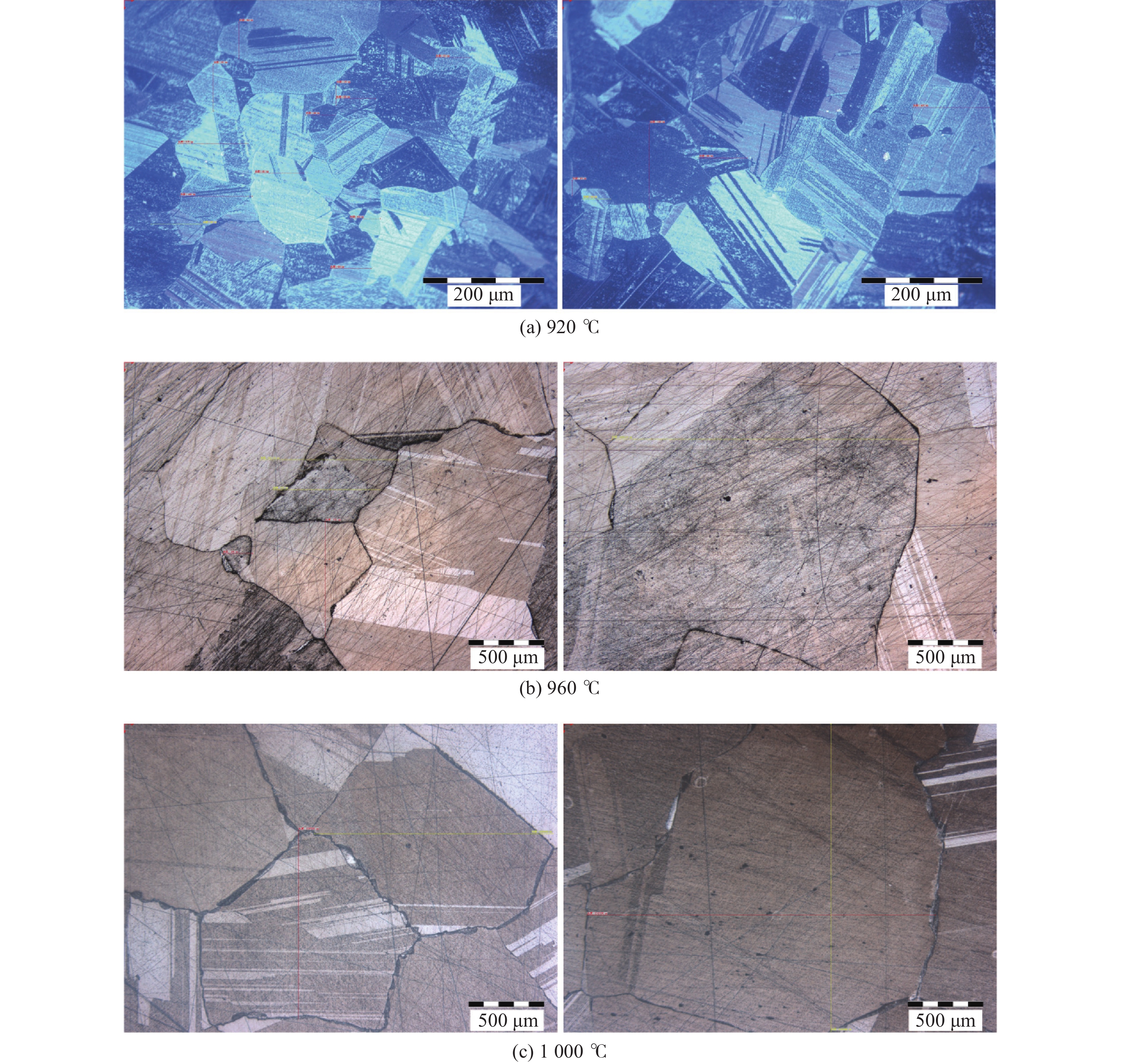
生长温度是指生长ZnSe晶体基板的温度,根据物理气相沉积的工艺原理,此温度为影响ZnSe晶体质量的关键因素。为了研究生长温度对PVDZnSe晶体尺寸的影响,选择920、960、1 000 ℃三个生长温度来进行样品沉积。图1是利用金相显微镜观察到的在三个不同生长温度下所制备样品的表面形貌,可以看出三种样品的晶粒尺寸存在明显差异。生长温度为920、960、1 000 ℃的ZnSe晶粒尺寸分别约为20~180、300~2 000、1 200~2 800 μm。可见随着生长温度的升高,PVDZnSe材料的晶粒尺寸也在变大。这是因为,随着生长温度的升高,粉体原料的蒸发速率增加,晶核在沉积基板上可以接触到更多的气体分子,从而加快了晶体生长速率。同时,晶粒还会将周围的小晶粒进行吞,即发生二次结晶现象。生长温度越高,晶粒的二次结晶现象就越明显。因此,ZnSe晶体材料的晶体尺寸随着沉积温度的增加而快速增大。生长温度越低得到的PVDZnSe材料晶粒尺寸越小。理论上讲,小晶粒尺寸利于优化ZnSe材料的可加工性。为了表征所制备材料的可加工性能,对材料的断裂韧性与硬度进行了测试,并根据测试数据对其脆性指数进行了计算。表1为不同温度条件下制备的PVDZnSe材料的可加工性数据情况,其中920 ℃条件下制备的PVDZnSe由于厚度较小,无法进行断裂韧性测试。从表1中可以看出,随着晶粒尺寸的增加,材料的硬度在缓慢增加,断裂韧性逐渐降低,所以其脆性指数在逐渐增加,可加工性能变差。

Figure 1. Surface morphology of PVDZnSe prepared at different temperatures
No. T/ ℃ Grain size/μm HV/GPa KIC/MPa·m1/2 HV/KIC/μm−1/2 1 920 20 -180 0.93 - - 2 960 300-2000 1.02 0.63 1.62 3 1000 1200-2800 1.07 0.46 2.32 Table 1. Machinability data of PVDZnSe materials prepared at different temperatures
但实验过程中发现,当生长温度为920、960、1 000 ℃时,PVDZnSe晶粒的生长速率分别为0.1、0.5、0.6 mm/h,即PVDZnSe生长速率会随着生长温度的降低而显著减慢。生长速率过于缓慢会延长晶体生长周期,导致生产成本增加,并且在长时间生长条件下,晶粒也会慢慢长大,0.5 mm/h被认为是最佳的生长速度。因此,从晶粒尺寸与生长速度两方面综合考虑,960 ℃为PVDZnSe的最佳生长温度。
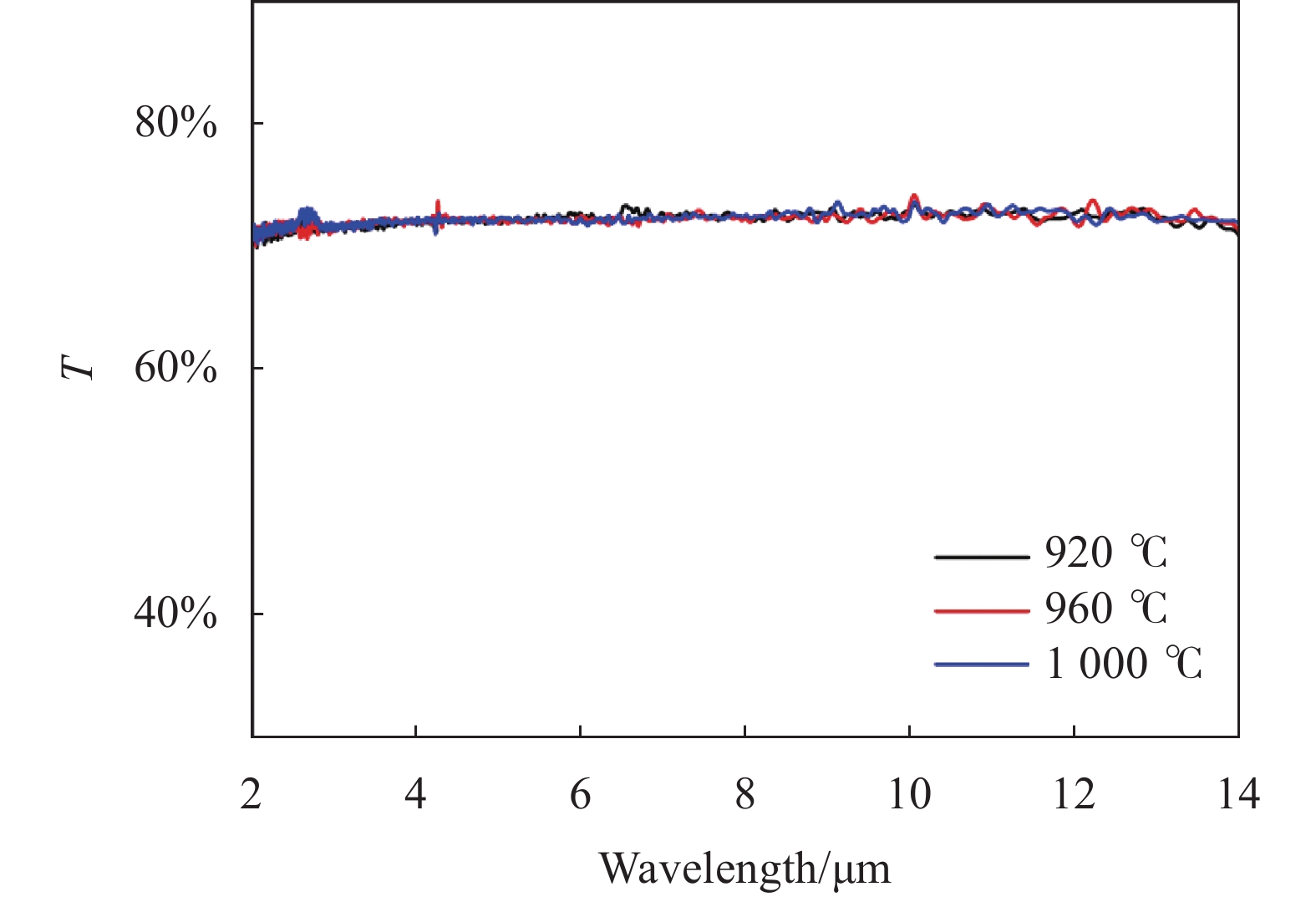
对上述三种PVDZnSe材料进行光学性能测试,测试结果如图2所示。在2~14 μm波长范围内,三种材料的平均透光率分别为70.1%、70.3%、70.2%。说明晶粒尺寸对PVDZnSe材料在2~14 μm波段范围内的光学透过率基本没有影响。

Figure 2. Optical properties of ZnSe materials at three differernt temperatures
-
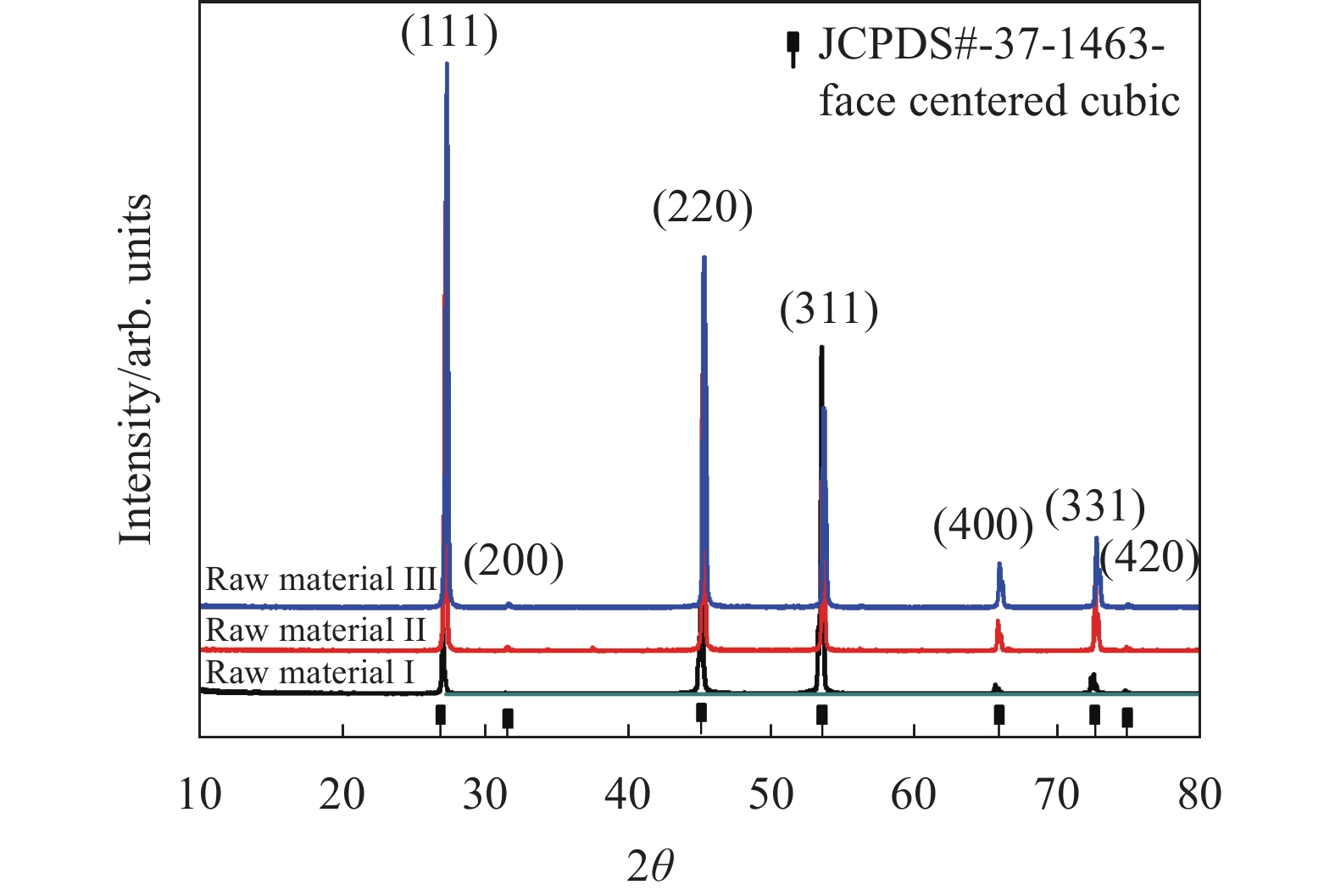
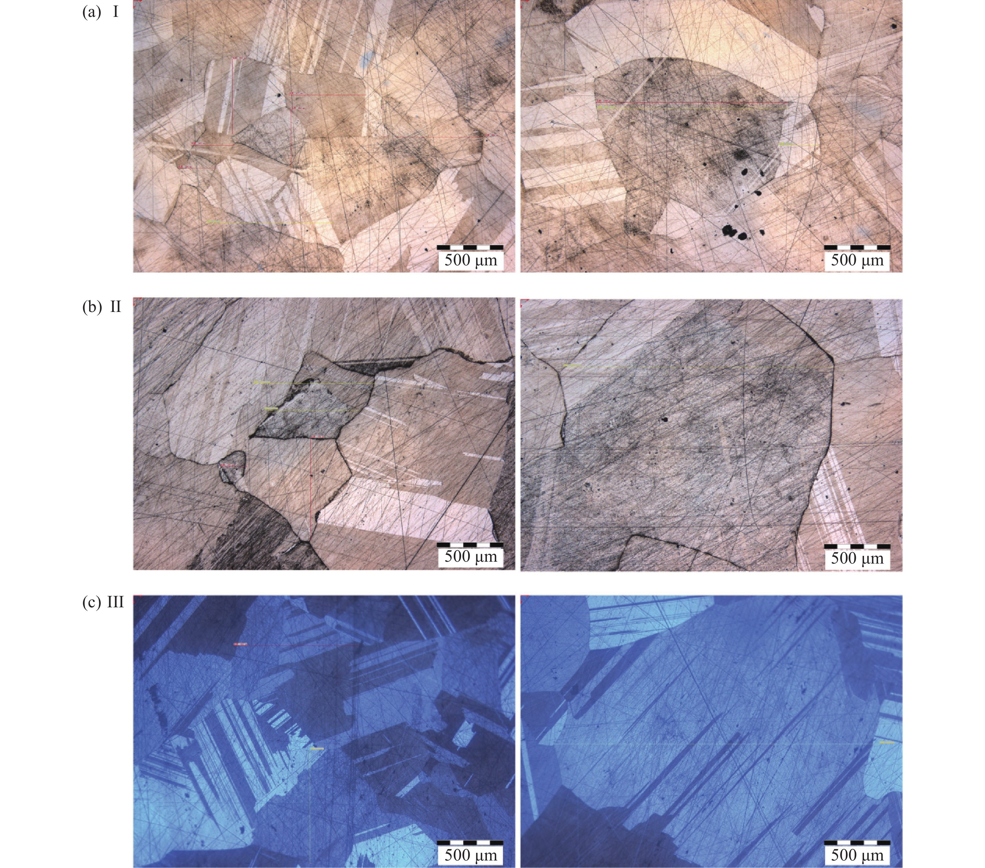
ZnSe的原料特性会影响其蒸发速率,而蒸发速率又会影响PVDZnSe材料的晶体生长过程进而影响材料的晶粒尺寸。对比分析相同沉积工艺条件下由不同ZnSe粉体原料制备的PVDZnSe材料的微观形貌。所选三种原料分别标记为Ⅰ、Ⅱ、Ⅲ,原料Ⅰ和Ⅱ为粉体原料,原料Ⅲ为块体材料。采用场发射扫描电子显微镜测得三种原料的微观形貌如图3所示。原料Ⅰ和原料II的微观形貌图放大倍数为5000×,是采用场发射扫描电子显微镜在5000×放大条件下获得。原料III为采用金相电子显微镜在50×放大条件下获得。从图3可以看出原料Ⅰ、Ⅱ、Ⅲ的晶粒尺寸范围分别为2~10 μm、10~20 μm和300~2 000 μm。

Figure 3. Micromorphology of the three raw materials
图4为所选三种原料的X射线衍射图。三种原料都在相同的位置出现衍射峰,与ZnSe的JCPDS 卡片库中PDF#37-1463标准卡片的特征峰位完全吻合。三种原料的晶粒尺寸尽管不同,但是均为微米级别,所以三种原料的XRD图谱均未出现宽化现象,峰型十分相似。
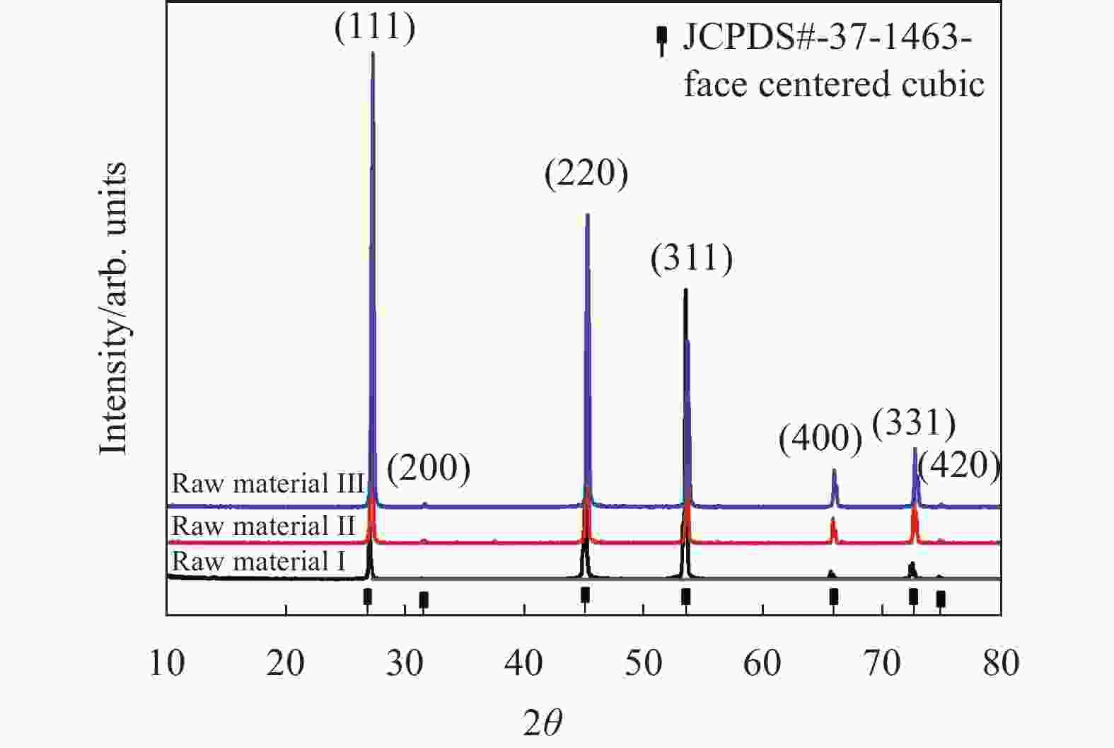
Figure 4. X-ray diffraction patterns of the three raw materials (I, II and III)
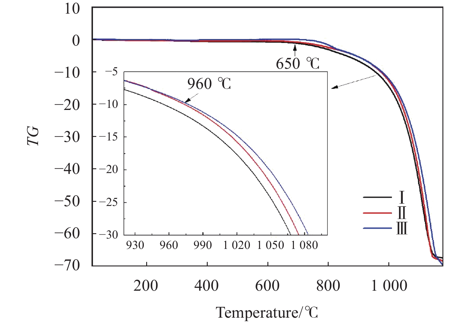
图5为利用金相显微镜观察到的三种原料在生长温度为960 ℃条件下制备出的PVDZnSe晶体材料的表面形貌图。从图中可以看出,采用Ⅰ、Ⅱ和Ⅲ三种原料制备得到PVDZnSe晶体材料的粒径分别为200~1 500 μm,300~2 000 μm以及880~2 500 μm。PVDZnSe晶体材料的粒径随着原料粒径的增加而呈现增加的趋势。这是因为,在相同温度下,原料粒径尺寸越大就越难蒸发,使得ZnSe气体分子在沉积基板上的生长速率远大于成核速率,沉积基板上的ZnSe晶核快速长大,从而导致晶粒尺寸偏大。图6为三种原料在室温至1200 ℃范围内的热重曲线。从图中可以看出,在760~820 ℃之间,三种原料的失重程度为原料Ⅰ>原料Ⅱ>原料Ⅲ。在820~940 ℃范围内,原料Ⅰ失重程度最大,原料Ⅱ和原料Ⅲ程度相近。在940~1 200 ℃之间,原料失重程度为原料Ⅰ>原料Ⅱ>原料Ⅲ。因此,可以推测出,当生长温度为960 ℃时,原料Ⅰ的蒸发速率最快,原料Ⅱ次之,原料Ⅲ最慢。这也解释了在相同制备工艺条件下,由原料Ⅰ制备的PVDZnSe晶粒尺寸最小的原因。

Figure 5. Surface morphology of PVDZnSe materials from three kinds of raw materials respectively under the same process
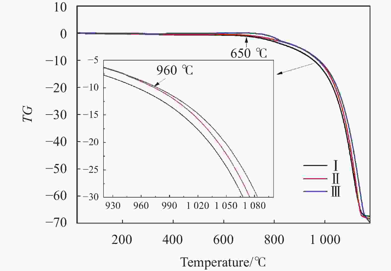
Figure 6. Thermogravimetric curves of the three kinds of ZnSe raw materials in the temperature range from room temperature to 1 200 ℃
表2为采用不同原料在相同生长条件下制备的PVDZnSe材料的可加工性数据情况,从表2中很容易可以看出,随着晶粒尺寸的增加,材料的硬度也在缓慢增加,断裂韧性逐渐降低,因此脆性指数增加,可加工性能变差。
No. Raw material Grain size/
μmHV/
GPaKIC/
MPa·m1/2HV/
KIC/μm−1/21 Ⅰ 200-1500 0.98 0.66 1.48 2 Ⅱ 300-2000 1.02 0.63 1.62 3 Ⅲ 880-2500 1.04 0.61 1.70 Table 2. Machinability data of PVDZnSe materials prepared with three kinds of raw materials
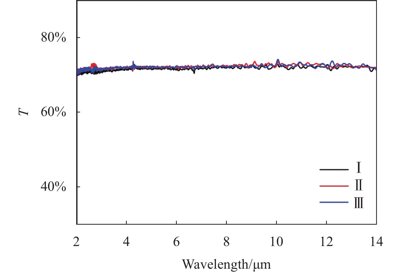
图7为三种材料的透过率曲线值。采用原料Ⅰ、原料Ⅱ和原料Ⅲ 制备的PVDZnSe材料的透过率分别为70.1%、70.3%、70.3%。可见原料尺寸对PVDZnSe的透过率影响不大。

Figure 7. Optical properties of PVDZnSe prepared with three kinds of raw materials under the same process
由PVDZnSe材料加工得到的光学零件实物样件如图8所示。

Figure 8. Sample of PVDZnSe optical parts
-
文中从生长温度与沉积原料两个方面,研究了制备工艺对其晶粒尺寸的影响。研究结果如下:
(1) 在选取的920、960、1 000 ℃三个温度条件下,随着沉积温度越来越高,所制备的PVDZnSe材料晶粒尺寸越来越大,晶粒尺寸分别为20~180、 300~2 000、1 200~2 800 μm。
(2) 在相同工艺参数条件下,选用粒径分别为200~1 500、300~2 000、880~2 500 μm的三种原料进行ZnSe材料的制备。随着沉积原料的晶粒尺寸越大,所制备的晶体尺寸越大。
(3) 随着晶粒尺寸的增加在不断增加,PVDZnSe材料的脆性指数增加,其可加工性能变差。
(4) 在可调节的晶粒尺寸范围内,晶粒尺寸对材料透过率的影响不大,都能达到70%以上。
Study of preparation process of PVDZnSe infrared optical materials based on different grain sizes
doi: 10.3788/IRLA20210565
- Received Date: 2021-08-12
- Rev Recd Date: 2021-12-30
- Publish Date: 2022-08-05
Fund Project:
National Natural Science Foundation of China (61905179,61975150);High-level Innovation team of Tianjin Talent Development Special Support Plan
-
Key words:
- PVDZnSe /
- grain size /
- deposition temperature /
- raw material
Abstract: ZnSe has always been one of the preferred materials for optical parts due to its excellent optical and mechanical properties. The manufacturing cost of optical parts such as optical windows and optical lenses largely depends on the machinability of optical materials, and processing costs account for more than 50% of the total manufacturing costs. The machinability of optical materials is related to the grain size. In this paper, the physical vapour deposition (PVD) method was employed to prepare PVDZnSe infrared optical materials, and the influence of the PVDZnSe preparation process on its grain size and machinability was investigated from the aspects of deposition temperature and raw material properties. It was demonstrated that under the three temperature conditions of 920 ℃, 960 ℃ and 1000 ℃, with the higher deposition temperature, the grain size of the PVDZnSe material showed an increasing trend, and the size ranges were 20-180 μm, 300-2000 μm and 1200-2800 μm, respectively. Under the same process parameters, the PVDZnSe materials were prepared from three different ZnSe raw materials with particle diameters of 2 -10 μm, 10-20 μm and 300-2000 μm. With the increase in grain size of the ZnSe raw materials, the grain size also increased. The results show that the grain size of the obtained PVDZnSe increases significantly, and the brittleness index also increases, which indicates that the machinability of PVDZnSe gradually worsens. The study also found that the influence of grain size on the transmittance of the PVDZnSe material is not significant. The average transmittance of the PVDZnSe material can reach more than 70% in the wavelength range of 2-14 μm. This study provides practical experience and technical support for the application of PVDZnSe optical parts.


 DownLoad: