


-
绝缘体上硅(Silicon on Insulator, SOI)材料平台因其与成熟的CMOS工艺兼容,可实现低成本、大规模量产的优势,广泛地应用于光子集成芯片设计之中。SOI波导结构的芯层Si与包层SiO2折射率相差很大,因此可在极小的弯曲半径时实现低损耗传输[1],这对进一步减小芯片尺寸,提高集成度十分有利。然而由于较大折射差率,SOI波导通常会引入较大的偏振模式色散[2]、偏振相关损耗及波长漂移[3]。在许多光传感、相干光系统中,如集成光学陀螺[4]、偏振相干探测系统[5]等,为了抑制偏振模式串扰/误差,仅允许某一特定偏振态的光传输,因此,片上偏振控制器件必不可少。波导偏振器可通过滤除一种偏振态,而保留其正交偏振模式,以简单的方式实现在光子回路中偏振透明传输。近年来,基于Bragg光栅结构的波导偏振器结构因其具有高偏振消光比、低损耗及大带宽等优势,成为研究的热点。2014年,戴道锌课题组[6]利用亚波长光栅在SOI波导上实现了27 dB的偏振消光比,损耗低至0.5 dB,但带宽较小;周治平课题组[7]提出了一种基于混合等离子Bragg光栅的偏振器结构,可有效缩短波导长度,2.5 μm即可实现25 dB的高消光比,但制作工艺极为复杂;2020年,Kazanskiy等[8]利用周期光栅结构实现了整个C波段大于28.5 dB的消光比,器件损耗约2 dB。传统的光栅偏振器为垂直光栅结构,反射光发生回耦,会引起较强的端面反射;且光栅参数通常需要多次仿真计算才能得到最优参数[9-10],设计过程相对复杂。
针对这些不足,文中提出了一种基于倾斜Bragg光栅的SOI波导偏振器结构,并利用一维光子晶体能带理论计算TM导带与TE禁带的重叠带隙,用于光栅设计,可快速得到最优参数,使得TE模式光经过光栅被高效反射,而TM模式以极低的损耗传输通过,实现超高偏振消光比与低损耗。此外文中还研究了Bragg光栅周期层数、光栅倾斜角及刻蚀宽度偏差等参数对偏振器的损耗、消光比及工作带宽等关键指标的影响,并进行了分析讨论。
-
SOI波导基本结构一般为Si衬底上生长一定厚度的SiO2绝缘缓冲层,中间为波导芯层Si (ncore=3.47),上包层为SiO2 (ncladding=1.444),产生超高折射率差。设计的超高消光比偏振器结构如图1所示,主要由SOI输入波导、倾斜Bragg光栅波导及输出波导三部分构成。倾斜Bragg光栅由Si与SiO2两种不同材料介质层周期排列构成。该结构仅需一次曝光刻蚀,制作工艺十分简单。

Figure 1. Schematic layout of titled Bragg grating-based polarizer on SOI waveguide
其中Bragg光栅周期为a,两种介质层的宽度分别为a1与a2,对应有效折射率分别为n1与n2。θ为Bragg光栅与光传输方向的倾斜夹角,ϕ为关于光栅界面法线方向的入射角,d为相应的周期间距。满足以下几何关系:
满足Bragg相位条件的光经过光栅发生高效反射,而其他部分光会透射传输,利用此原理可实现TE与TM模式的分离。
-
Bragg光栅由宽度分别为d1与d2的两种介质层交替组成,结构如图2所示。利用一维光子晶体能带理论可计算相应Bragg光栅的带隙分布,准确地进行光栅参数设计。

Figure 2. Properties of light propagated in one-dimensional photonic crystal structure
光在两种介质层中的场E1、H1与E2、H2关系可由传输矩阵 [11]表示:
经过一个周期,传输矩阵为:
式中:
${\delta _i} = \dfrac{{2\pi }}{\lambda }{n_i}{d_i}\cos {\phi _i}{\text{ (}}i{\text{ = 1,2)}}$ ; p取值与偏振模式相关,对于TE模式:${p_i} = \sqrt {{{{\varepsilon _i}} \mathord{\left/ {\vphantom {{{\varepsilon _i}} {{\mu _i}}}} \right. } {{\mu _i}}}} \cos {\phi _i}$ ;而对于TM模式:$ {p_i} = \sqrt {{{{\mu _i}} \mathord{\left/ {\vphantom {{{\mu _i}} {{\varepsilon _i}}}} \right. } {{\varepsilon _i}}}} \cos {\phi _i} $ 。根据Bloch-Fouquet理论,Bloch波矢K满足关系:
利用Bloch波矢K的取值,可判断光在一维光子晶体结构中的传输状态。若K为实数,即
${{\left| {{{{m}}_{{\text{11}}}} + {{{m}}_{{\text{22}}}}} \right|} \mathord{\left/ {\vphantom {{\left| {{{{m}}_{{\text{11}}}} + {{{m}}_{{\text{22}}}}} \right|} 2}} \right. } 2} \lt 1$ ,对应光子晶体导带;若K为虚数,相应满足${{\left| {{{{m}}_{{\text{11}}}} + {{{m}}_{{\text{22}}}}} \right|} \mathord{\left/ {\vphantom {{\left| {{{{m}}_{{\text{11}}}} + {{{m}}_{{\text{22}}}}} \right|} 2}} \right. } 2} \gt 1$ ,则光处于消逝态(光子晶体禁带),从而得到一维光子晶体的能带分布[12]。对角频率
$\omega $ 关于$2\pi c/d$ (2π/d为一维光子晶体的倒易空间点阵基矢)进行归一化,得到归一化频率$\varpi $ 表达式为:式中:c为真空中光速;λ为真空中波长。取介质层宽度比例h=d1/d,则d2=d(1-h)。波矢的平行分量ky由基矢2π/d表示为
${k_y} = k' \cdot ({{2\pi } \mathord{\left/ {\vphantom {{2\pi } d}} \right. } d})$ 。给定h,结合公式(3)与(4),根据Bloch波矢K的取值,可以计算得到两种偏振模式下一维光子晶体在$\omega - {k_y}$ 平面上的能带分布,如图3所示(灰色区域为导带,白色区域为禁带)。
Figure 3. Band structure distribution of one-dimensional photonic crystal
当ky=0时,ϕ=0,对应垂直入射。图中横坐标数值
$k{'}={k}_{y}\cdot(d/2\pi)$ ,纵坐标的数值$\varpi =\omega \cdot \left(d/2\pi c\right)$ ,则$\varpi ,k{'}$ 之间的关系为:则
$\varpi - k'$ 直线的斜率即为$1/{n_1}\sin \phi $ ,由此可得到不同入射角ϕ下光子带隙的分布。选择ϕ角入射时,TE模式禁带的下边界(${\varpi _1}$ )与TM模式导带的上边界(${\varpi _2}$ ),即可得到重叠带隙。根据公式(5),$d$ 为常数,归一化角频率${\varpi _1}\sim{\varpi _2}$ 对应的波长范围为:取偏振器工作的中心波长
${\lambda _0} = ({{{\lambda _1} + {\lambda _2})} \mathord{\left/ {\vphantom {{{\lambda _1} + {\lambda _2})} 2}} \right. } 2}$ ,从而Bragg光栅周期可由以下公式确定:再根据公式(1),即可确定倾斜光栅周期a、倾斜角θ等结构参数,从而实现倾斜Bragg光栅型波导偏振器的设计。
上述方法利用能带理论来设计光栅参数,也可对光在波导中的传输特性进行分析。为实现TE模式高效反射,TM低损传输,应满足如下Bragg条件:
式中:
${n_1}^{\rm TE}、{n_1}^{\rm TM}、{n_2}^{\rm TE}、{n_2}^{\rm TM}$ 分别为TE与TM模式在相应介质层的有效折射率,可通过数值仿真计算得到。利用上式可以验证能带理论设计参数的可靠性。 -
设计SOI波导的尺寸为500 nm×220 nm,偏振器工作的中心波长λ0=1550 nm,h=0.75,利用一维光子晶体能带理论计算得到Bragg光栅的TE与TM模式带隙分布(见图3)。选择入射角ϕ=25°,作
$\varpi = 1/{n_1}\sin {25^ \circ } \cdot k'$ 直线与能带结构相交,由此可得到TE模式禁带与TM模式导带的重叠带隙上下边界分别为:${\varpi _1} = $ 0.2302,${\varpi _2} $ = 0.2508,根据公式(8)可得到Bragg光栅周期d=372.1 nm。从而θ=65°,a=410.6 nm。根据上述参数构建模型,利用MODE Solutions (FDE)软件可分别计算TE与TM模式光在波导结构中传输的有效折射率,
${n}_{1}{}^{\rm TE}\text{=}2.442,\text{ }{n}_{1}{}^{\rm TM}\text{=}1.766$ ,根据公式(9)计算有:TM模式${L_B}^{\rm TM} = 561.7 \lt {\lambda _0}/{2} = 775$ ,对于TE模式${L_B}^{\rm TE} = 777.6$ ,基本满足Bragg条件,验证了计算参数的准确性。 -
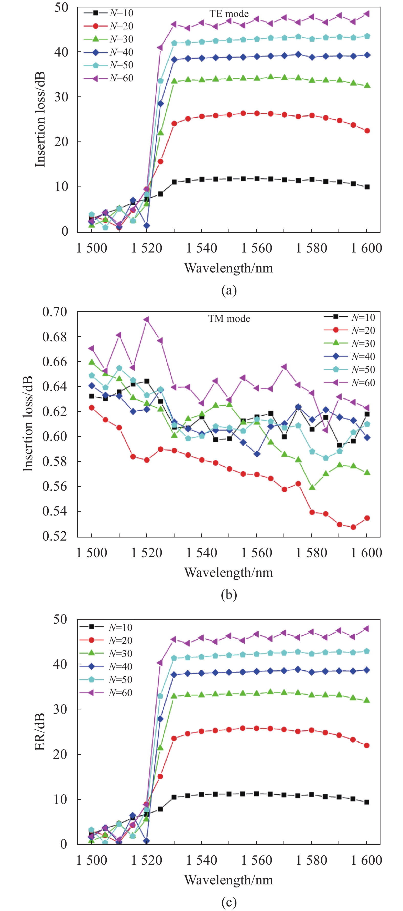
周期层数对光传输效率有很大的影响,改变周期层数N,从10层依次增加至 60层(间隔为10层),利用FDTD Solutions软件进行3D建模仿真,仿真波长扫描范围从1500~1600 nm (间隔5 nm)。TE与TM模式经过倾斜Bragg光栅波导传输透射效率分别为TTE,TTM,则TM光栅偏振器的消光比为TE模式与TM模式的传输损耗之差,ER=10 log10 (TTM/TTE),偏振器附加损耗为TM模式的传输损耗IL=−10 log10TTM。仿真得到了TE模式与TM模式光经过不同周期层数倾斜Bragg光栅波导的损耗,并计算偏振器的消光比,如图4所示。

Figure 4. Transmission properties of waveguide polarizers with different Bragg grating periods. (a) TE mode loss; (b) TM mode loss; (c) Extinction ratio of polarizer
N=10时,中心波长1550 nm处TE传输损耗>11.8 dB;随着光栅周期层数增加,TE模式的损耗迅速增加,当N增加至60层时,传输损耗>46.8 dB,此时光几乎被完全反射。而对于TM模式光,绝大部分光透射传输,随着周期层数的增加, 传输损耗增量<0.12 dB。
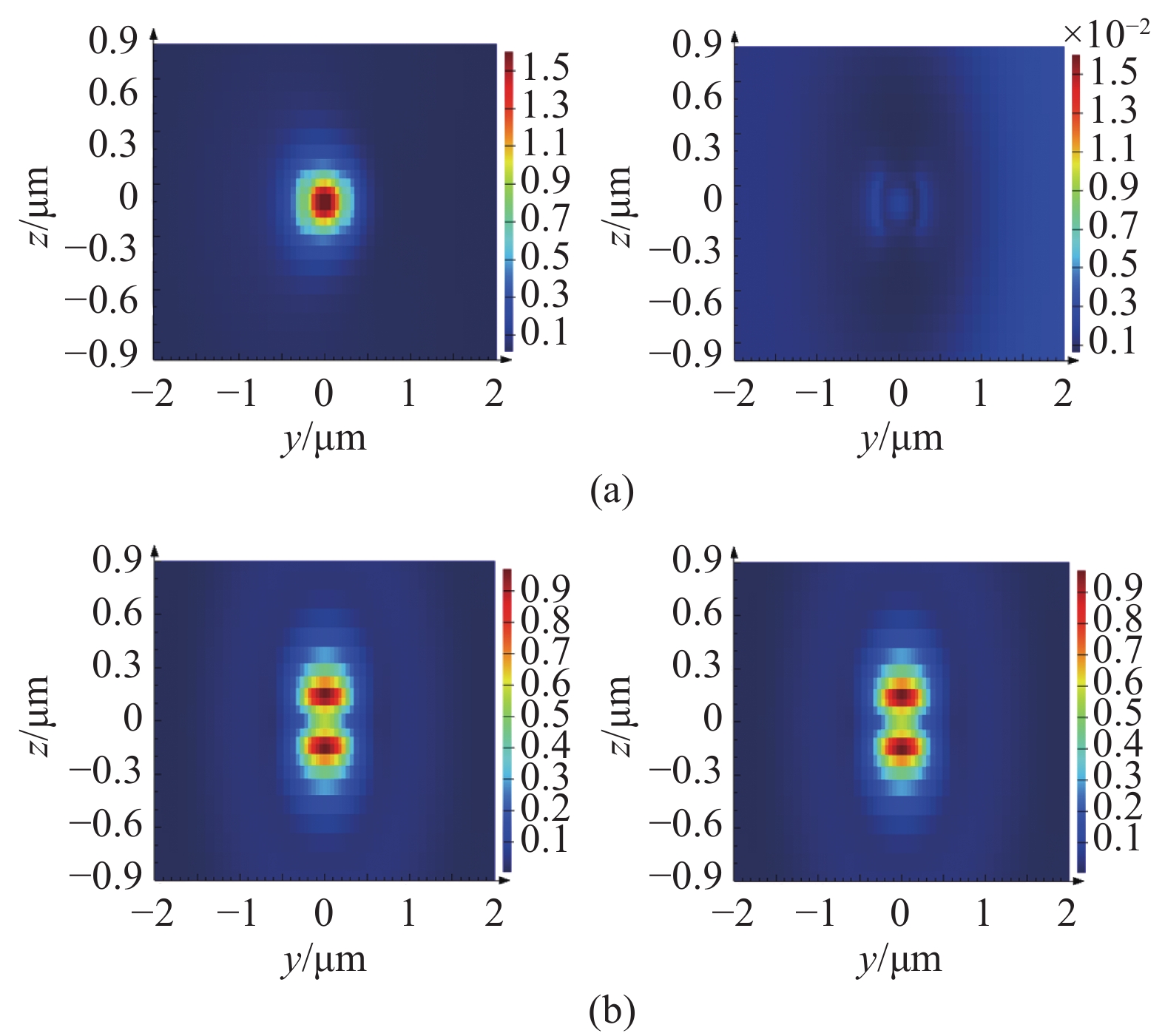
从仿真结果可知,当周期层数由30增加至40层时,中心波长处消光比由33 dB进一步提高至38 dB (满足大部分应用需求),而器件损耗几乎不发生变化。考虑波导尺寸,选择N=40设计光栅,此时Bragg光栅波导的长度约16 μm,可实现C波段及L波段70 nm的带宽内>37.6 dB的超高消光比,损耗小于0.64 dB。仿真得到了TE与TM模式光在经过Bragg光栅偏振器传输的模场分布变化,如图5所示,可以直观发现TE模式光经过Bragg光栅后迅速衰减,而TM模式几乎没有变化。图6中TE与TM模式沿光传输方向的场分布也能说明TE模式接近完全反射,TM模式低损传输,从而产生高消光比。

Figure 5. Variations of mode field distributions of light for (a) TE and (b) TM mode at center wavelength propagated in Bragg grating polarizer

Figure 6. Field distributions of light along propagated direction for TE and TM mode
-
仿真得到了不同倾角偏差下光栅偏振器的TE与TM模式传输损耗,并计算消光比,如图7所示。当Δθ从−5°变化至5°时,TE模式的高反射带(传输损耗大)往长波方向移动;TM模式传输损耗逐渐降低。Δθ=−5°时,偏振器可实现1510~1585 nm波段大于30 dB的消光比;当Δθ=5°时,偏振器在1545~1600 nm波段消光比大于30 dB,有效工作带宽变窄。这种变化趋势可根据光子晶体能带结构(见图3)解释说明,Δθ从−5°变化至5°,对应Δϕ从5°变化至−5°,此时TE模式禁带边界
$\varpi $ 的值变小,且禁带宽度变窄。当周期d不变时,根据关系$\varpi {\text{ = }}d/\lambda $ ,禁带边界波长增大,带宽减小。而当Δθ从0变化至2.5°时,高消光比有效带宽几乎不变,器件损耗由0.61 dB减小至0.55 dB,故可取Δθ=2.5°以得到最优性能。
Figure 7. Transmission properties of Bragg grating-based polarizers with different titled angle deviations. (a) TE mode loss; (b) TM mode loss; (c) Extinction ratio
综上所述,光栅倾角的变化会对偏振器的工作波段及带宽产生影响,但在一定偏差范围内仍能保证偏振器在中心波长附近的性能。
-
刻蚀层宽度a2的偏差也会对偏振器性能产生重要影响,仿真中分别取h=0.70、0.72、0.75、0.78、0.80,得到不同宽度下TE与TM模式传输损耗及消光比,如图8所示。

Figure 8. Transmission properties of Bragg grating-based polarizers with different width ratios. (a) TE mode loss; (b) TM mode loss; (c) Extinction ratio
当h从0.7增加至0.8时,刻蚀宽度a2逐渐变小,TE模式的高反射(传输损耗大)带往长波方向移动,对偏振器工作波段影响明显。在h取值较小时,偏振器能够在宽波段范围内保持高消光比,而TM模式的传输损耗略有增加;当h不断增大至0.80时,在中心波长1550 nm处,消光比<4 dB,性能已不满足设计需求。但当h=0.72与0.78,对应刻蚀宽度偏差Δa2=±12 nm,此时偏振器仍能保持在中心波长附近较大的带宽内的高消光比,且附加损耗波动较小,表明设计的器件具有较好的误差容限。
将上述仿真结果与国内外相关研究报道 [13-14]对比表明:在波导长度相近的前提下,设计的倾斜Bragg光栅波导偏振器在性能方面具有更大优势,能够实现高消光比、低损耗及大带宽。且该结构基于常用的220 nm芯层的SOI平台设计,工艺简单成熟,设计的结构具有较好的刻蚀误差容限,故器件加工难度低。后续工作可推进非均匀周期准啁啾光栅设计[15],以进一步增大工作带宽,并实现该偏振器结构在更多相关领域应用[16]。
-
文中提出了一种基于倾斜Bragg光栅的紧凑型SOI波导偏振器结构,并利用一维光子晶体能带理论分别计算Bragg光栅的TE模式与TM模式带隙分布差异,确定结构参数,保证TM模式光在Bragg光栅中低损透射传输,而TE模式被高效反射,实现在70 nm大工作带宽内保持>37 dB超高偏振消光比。相比传统Bragg光栅结构及设计方法,该偏振器能够减小端面反射,参数设计更加灵活准确。同时加工工艺简单,刻蚀误差分析表明其具有较好的加工误差容限。该结构在相干光探测、光传感等对片上偏振串扰抑制要求极高的领域,具有很大的应用潜力。
Design of Bragg grating-based ultra-high extinction ratio polarizer on silicon-on-insulator waveguide
doi: 10.3788/IRLA20210713
- Received Date: 2021-09-26
- Rev Recd Date: 2021-12-28
- Publish Date: 2022-08-31
-
Key words:
- polarizer /
- Bragg grating /
- one-dimensional photonic crystal /
- SOI waveguide
Abstract: The waveguide polarizer is a key component of an on-chip integrated coherent optical system, and it has attracted much interest to design a waveguide polarizer with an ultrahigh extinction ratio, low excess loss and compact size in photonic integrated circuits. A tilted Bragg grating-based polarizer on a silicon-on-insulator platform was proposed and designed by one-dimensional photonic crystal band gap theory. The energy band structure distribution for the TE and the TM modes were calculated using the energy band theory of one-dimensional photonic crystals, and the overlap gap between the forbidden band of theTE mode and the transmission band of the TM mode were used to determine the grating structure parameters. As a result, the TM mode light could pass through the Bragg grating waveguide with a low excess loss, while the TE mode shows almost complete reflection, introducing an extremely high polarization extinction ratio. The 3D FDTD simulation results suggest that a 16 μm titled Bragg grating-based waveguide polarizer could achieve an ultrahigh extinction ratio of more than 37 dB at the central wavelength of 1550 nm over a broad bandwidth of 70 nm, and the excess loss of the device is less than 0.64 dB. With an increasing length of waveguide to 25 μm, the extinction ratio could further reach up to 46 dB. The effects of the tilt angle and etching deviation on the performance of the polarizer were also studied, and the results show that the designed structure has a good fabrication tolerance. In addition, the polarizer only needs one-step etching with a simple fabrication process.


 DownLoad: