


-
光电探测器是将光信号转换为电信号的基本器件,是获取光信息的重要技术手段,已广泛应用于现代化生活的诸多领域。光电探测器依据基本原理可以分为光子型探测器和光热型探测器,依据探测波段可以分为可见光、近红外、中红外、长波红外及复合波段探测器。红外探测成像器件虽已应用于军事、工业、医学等多个方面,但其材料及器件性能研究相对可见光仍然不足,因此如何提升红外波段探测器性能及拓展红外探测器材料体系成为重要研究方向[1-2]。
二维石墨烯材料具有宽波段吸收(紫外到远红外)、载流子迁移率高、功函数可调、导热性好等突出优点,使其非常适用于红外探测器件制备[3]。然而,单原子层厚度的石墨烯对光的吸收率低,导致石墨烯器件的响应度被限制在mA/W量级[4]。此外,由于石墨烯的零带隙和高电导率,导致探测器暗电流较大,严重影响探测器灵敏度和探测波段。
为了充分利用石墨烯的优势并提升探测探测器灵敏度和响应波段,研究者们提出了包括石墨烯掺杂、微腔增强吸收和局域场调控等方法解决这一问题[5]。局域场增强可以简单描述为通过微观局部空间中的强场增强光-物质的相互作用和控制二维半导体中的载流子运动来有效的挑战器件性能,局域场增强的方式主要包括:光栅场增强、铁电场增强、浮栅感应静电场增强、层间内建场增强、温度梯度场增强和表面等离子体增强[6-7],这些局域场通过增加光吸收、提高载流子分离效率抑制噪声和放大光电增益来提高二维半导体探测的探测能力。其中基于光栅效应(Photogating effect)的局域场调控是一种有效提升石墨烯探测性能的方法,其可以简单描述为复合材料增强光吸收,并与石墨烯构筑局域场,形成光生载流子的局域限制或载流子向石墨烯沟道的注入,从而提升石墨烯的光响应电流变化,提升探测器性能及拓宽探测波段[8]。文中总结了近期局域场增强石墨烯近红外光电探测器相关的研究成果。简单介绍了单吸收层及双吸收层局域场增强石墨烯光电探测器件,分析基于不同类型感光材料器件的优缺点,对双吸收层器件对电流极性影响等相关研究进行了介绍,最后对局域场增强探测器在器件功能拓展领域的研究进行了简介。
-
初期研究者们设计单组分材料作为吸光材料,包括量子点、二维材料、有机小分子/聚合物、单晶、钙钛矿等,将单一吸光材料与石墨烯构筑局域场增强探测器灵敏度。2012年,Konstantatos等在石墨烯表面旋涂一层PbS量子点, PbS量子点充当局域光栅层,石墨烯为载流子传输沟道,器件结构如图1(a)所示。由于PbS量子点的宽光谱吸收特性,器件探测范围拓展到1 600 nm,更重要的是,器件表现出极高增益(高达108)特性,响应度达到107A/W,该成果充分验证了局域场光栅效应在低维材料探测体系中的重要作用[9]。实现增益的原因是量子点材料吸收光产生长寿命光生载流子,石墨烯与量子点形成的内建场促使空穴载流子注入石墨烯并在偏压下流向电极,另光生电子在量子点层形成局域光栅场增强空穴从电极的注入,使器件实现高增益(G=τlife/τtransit,τlife表示载流子寿命,τtransit表示载流子渡越时间)。近年由于钙钛矿具有直接带隙、高吸收系数、高载流子迁移率等优点,在光伏领域受到广泛关注。Lee等人利用溶液处理的钙钛矿材料CH3NH3PbX3作为光敏层,制备以钙钛矿为局域光栅场的石墨烯探测器[10],如图1(b)所示。由于石墨烯与钙钛矿层之间的有效载流子转移,器件实现可见到近红外的光谱探测(400~980 nm),在弱光探测条件下,响应度与外量子效率达180 A/W和5×104。有机材料由于具有成本低、大面积可延展、调控性高等优点,也是常见的光吸收材料。2021年,Miao Yu等人制备了基于有机聚合物PDVF-石墨烯混合光电探测器,通过简单的热处理,调控石墨烯费米能级及聚合物形态,从而实现了350~850 nm光谱探测[11]。多样化的二维材料相继成为研究者的探索热点,人们利用其他二维材料与石墨烯相结合来提升光响应度。2017年,Wenzhi Yu将MoTe2作为光栅层,石墨烯作为快速传输通道,光生电子被捕获在MoTe2层中引起光栅效应,使器件表现出高探测率(1.55×10¹¹ J)与高增益(4.69×10⁸),此外器件具有宽光谱检测范围(可见-近红外),在1 064 nm探测波长下,器件仍表现出970.82 A/W的高响应度[12]。量子点、钙钛矿、有机材料等能采用简单的旋涂或蒸镀工艺进行器件的制备,在柔性、大面积、低成本光电探测器领域有极大的应用潜力,而二维材料形成局域场大多需要机械剥离,难以实现阵列化均匀制备。此外可以通过控制量子点的尺寸实现中红外吸收,然而由于带隙的限制,单体有机及钙钛矿材料的吸收大多限制在可见到近红外(1 000 nm)。这些研究证明单光栅层的存在能捕获光生载流子使器件实现高增益,但由于缺乏内建电场及缺陷态的存在,由单吸收光栅层组成的石墨烯光电晶体管通常以较长的响应时间为代价。

Figure 1. Typical structure of single absorption layer graphene detector based on localized filed enhancement. (a) Structural diagram of the graphene/PbS phototransistor; (b) Structural diagram of the graphene/perovskite phototransistor; (c) Structural diagram of the graphene/PDVF phototransistor; (d) Structural diagram of the graphene/MoTe2 phototransistor
除了通过单组分材料与石墨烯形成的光栅局域场提高石墨烯探测器响应度,等离激元结构形成局域场增强也是提高二维材料光电探测器的有效策略。研究者将石墨烯等二维材料与金属纳米结构相结合,由于二维材料表面等离激元产生的局部电磁场可以有效增强光的吸收,从而使器件的性能及光谱选择性得到显著提高。2011年,Yuan Liu等人将石墨烯与金纳米颗粒相结合,相关结构如图2(a)所示,外量子效率达1.5%,比当时传统光电探测器的外量子效率提高了一个数量级[13]。此外,研究者将有纳米颗粒器件与无纳米颗粒器件进行对比,前者光响应度达2.2 mA/W,较后者提高400%。2017年,Zhenyi Ni等人制备了硅量子点-石墨烯探测器,结构如图2(b)所示,在不同的波段,器件的响应机制有所不同,在硅量子点的吸收波段范围内(紫外到近红外),器件的响应机制主要是光栅效应;而在中红外波段,量子点表面的等离激元引起的局部电磁场会增强石墨烯对中红外光的吸收,从而提高器件在中红外波段的响应[14]。这些研究表明基于石墨烯的等离激元形成的局域场增强促进了红外宽光谱探测技术的发展。
-
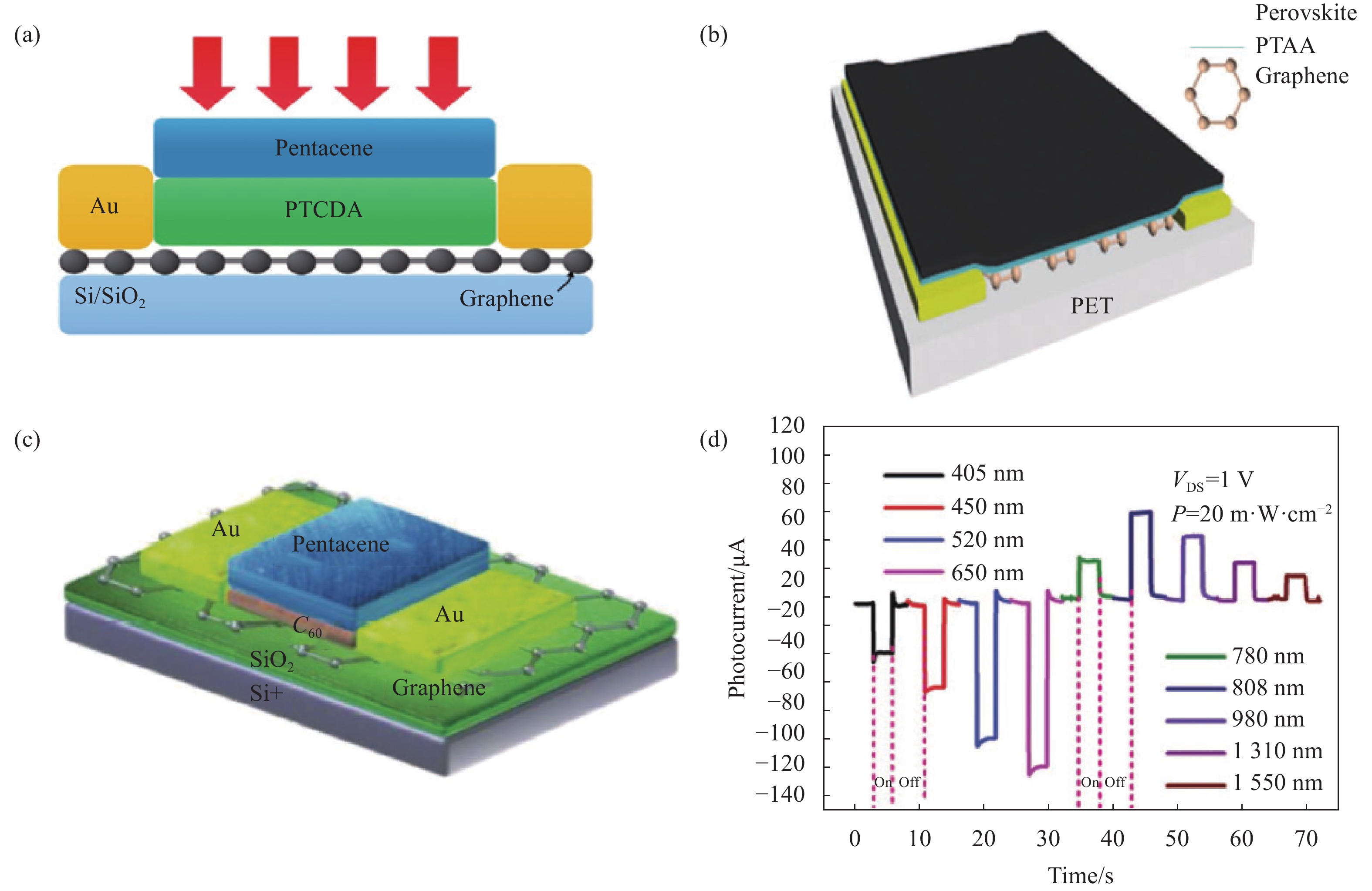
单吸收层材料形成的局域场注入能力受限,设置异质结形成内建局域场能够更有效分离产生的光生载流子,进而提升器件的光电特性。2017年,Xinran Wang等提出用有机异质结(PTCDA/并五苯)作为吸光层[15],如图3(a)所示,由有机吸收层产生电子-空穴对,在局域内建电场的作用下,促进电子空穴对的有效分离,部分光生电子注入石墨烯沟道,在石墨烯的传导作用下形成光电流,从而提升石墨烯基光电晶体管的性能,响应时间低至28 μs,响应度可达105A/W。利用具有高光吸收以及强载流子束缚特性的钙钛矿材料也实现了局域场有效调控的高响应性[16],如图3(b)所示,并且运用柔性衬底和溶液制备的路线使其在柔性可穿戴设备上具有应用前景。但是此类器件吸收波段仍限制于可见光波段,需通过合理选择双吸收层体系实现近红外波段的有效探测。
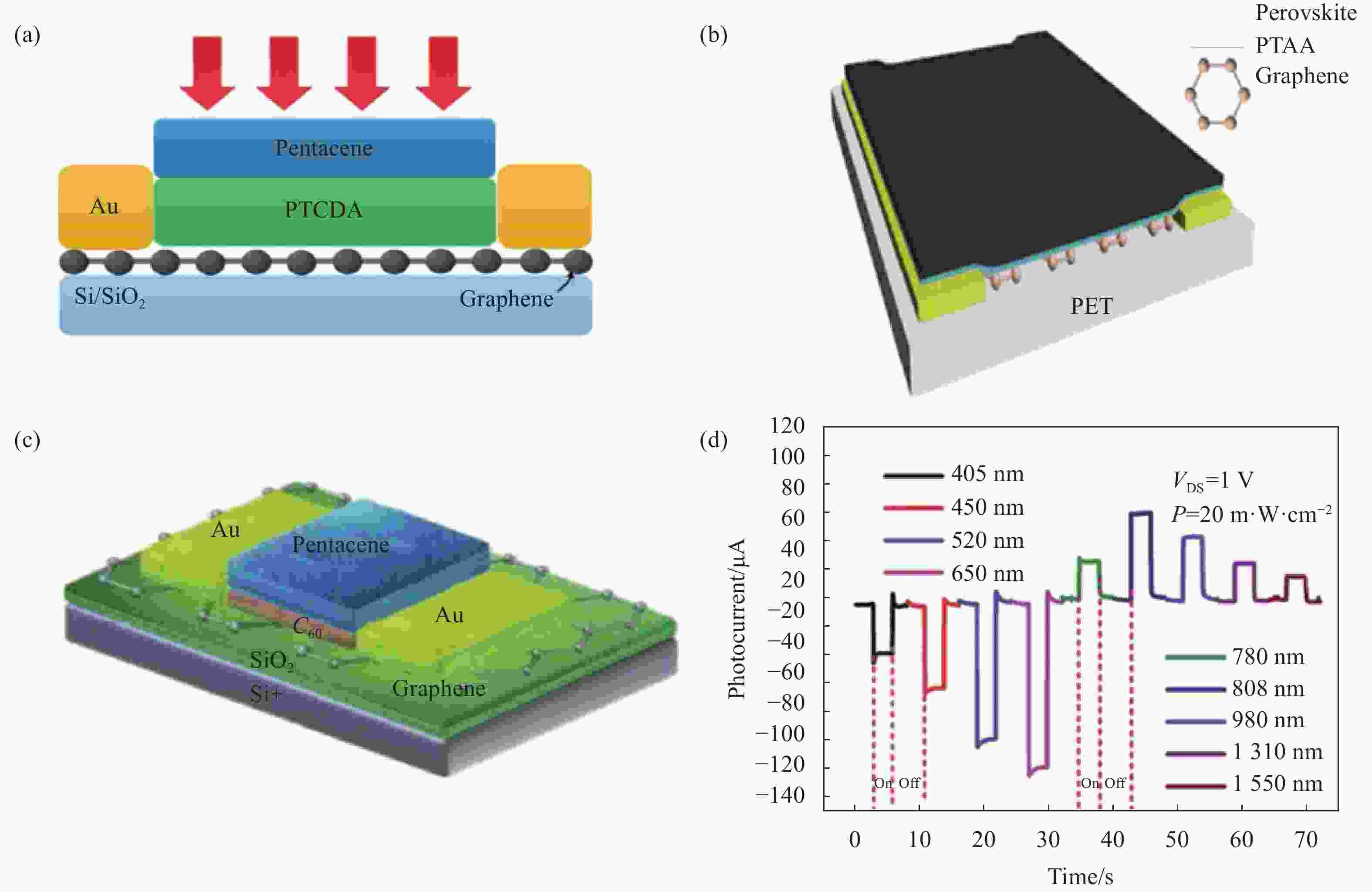
Figure 3. Typical structures of graphene detectors enhanced by localized field with double absorption layers. (a) Structural diagram of the graphene/PTCDA/pentacene phototransistor[15]; (b) Structural diagram of the graphene/PTAA/perovskite phototransistor[16]; (c) Structural diagram of the graphene/C60/pentacene phototransistor[17]; (d) Response characteristics with different wavelengths[18]
2018年,Jun Wang等人制作出了将C60与并五苯作为双吸收层的器件[17],结构如图3(c)所示。由于两种不同的吸收层材料在不同波长处的吸收特性的差异,该器件可在可见光与近红外光范围显示出双极性光响应(bi-directional photoresponsivity)的新颖特性,这也是首次在石墨烯基光电二极管发现了双极性响应,在可见光405~650 nm实现负响应,近红外波段780~1 550 nm表现为正响应,如图3(d)所示。正是利用双向极性响应的特性,相较于之前研究结果,实现了可见光到近红外光(405 ~1 550 nm)的宽波段探测,探测器响应度可达9 127 A/W,响应时间为275 μs,光电导增益可达5.2×10⁵。在此基础上,Jun Wang课题组继续通过调节中间层C60的厚度,研究石墨烯光电晶体管在不同波长处的光电流极性现象,研究结果表明光电流极性与波长甚至探测光强度密切相关,由于与光强相关的双极性现象,使该器件在正负极性转变处观察到明显的响应度-功率密度关系弯折现象[18]。Jun Wang课题组对电流极性的研究结果有助于探明多层系统中的电荷转移机制,并开发高速石墨烯光电晶体管。
前述研究中说明了与石墨烯形成光栅结构的光电导探测器吸收材料能带对电流极性有重要影响。Jun Wang等通过更换上层吸光材料为Bi2O2Se的石墨烯探测器,其响应范围可拓展至1 550 nm,基于Bi2O2Se的展示的复杂能带关系,系统解释了基于能带匹配造成波长依赖性的光电流极性改变的现象,器件光电流随入射波长变化展现出四种不同极性变化[19]。除此之外,通过引入HAT-CN与Bi2O2Se构成Ⅲ型结的石墨烯光电晶体管可极大地提高操作带宽[20]。与单独的石墨烯/Bi2O2Se相比,这些研究引入中间传输层使得器件性能显著提高,在探索多层结构器件的电荷转移机理和电流极性调制方面显示出巨大潜力。
为了进一步改善局域场对石墨烯的载流子注入能力,提升石墨烯光电导探测器探测性能, Jun Wang等将有机光伏器件中ZnO电子提取层引入到石墨烯沟道上[21],结构如图4(a)所示,并采用近红外吸光有机三元体异质结作为光敏层,采用工艺简单的溶液法制作器件,成功实现了6.1×10⁶ A/W的高响应度和2.4×1013 J的比探测率,在850 nm光照下的最小探测功率可达1.75 nW /cm2。基于其优良的近红外检测性能,可实现无外部电路支持的非接触式脉搏监测,实时通过手指监测人体脉搏跳动信号,如图4(b)所示,此外该器件还实现了电可擦光存储功能。这些研究通过低成本工艺和多层结构设计,为近红外区域提升光电晶体管的探测性能和多功能应用开辟了新的途径。
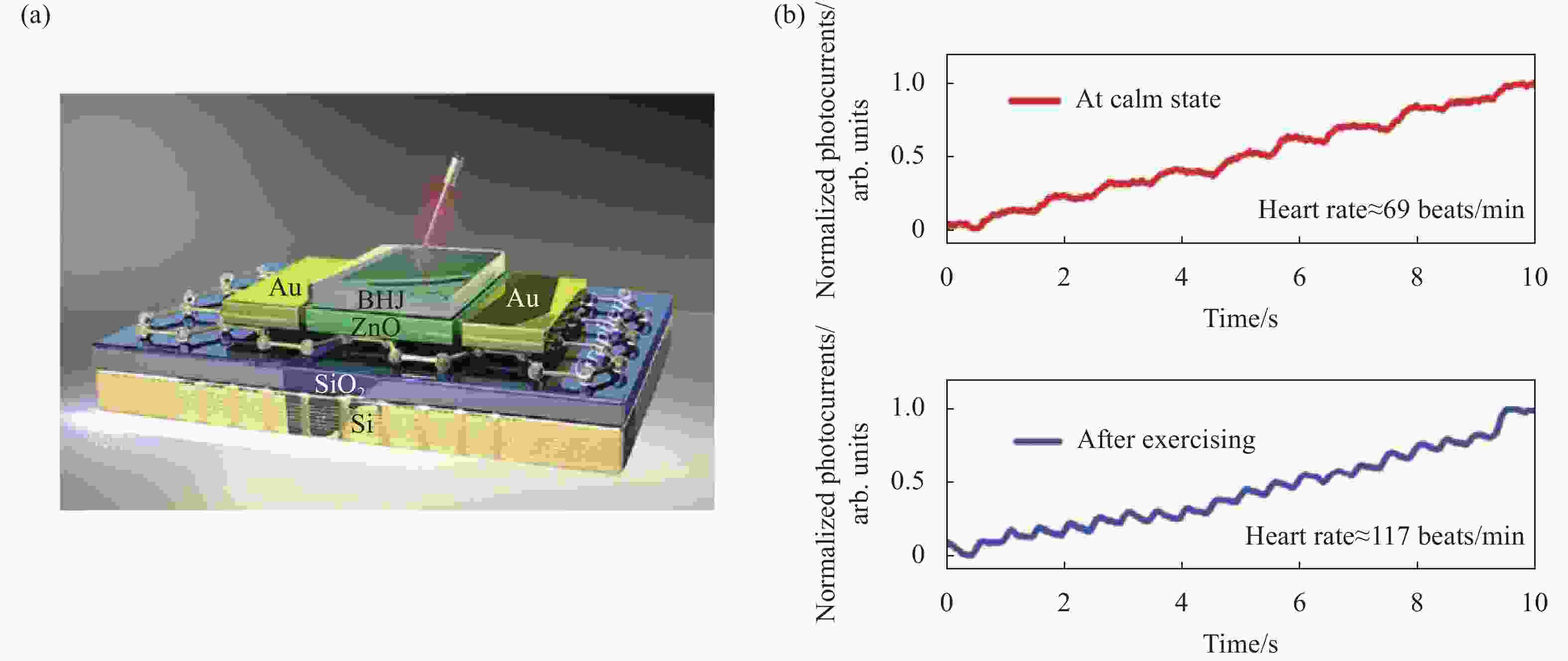
Figure 4. Injection layer structure NIR graphene/organic phototransistor. (a) Structural diagram; (b) Pulse signals in calm state and after exercise[21]
-
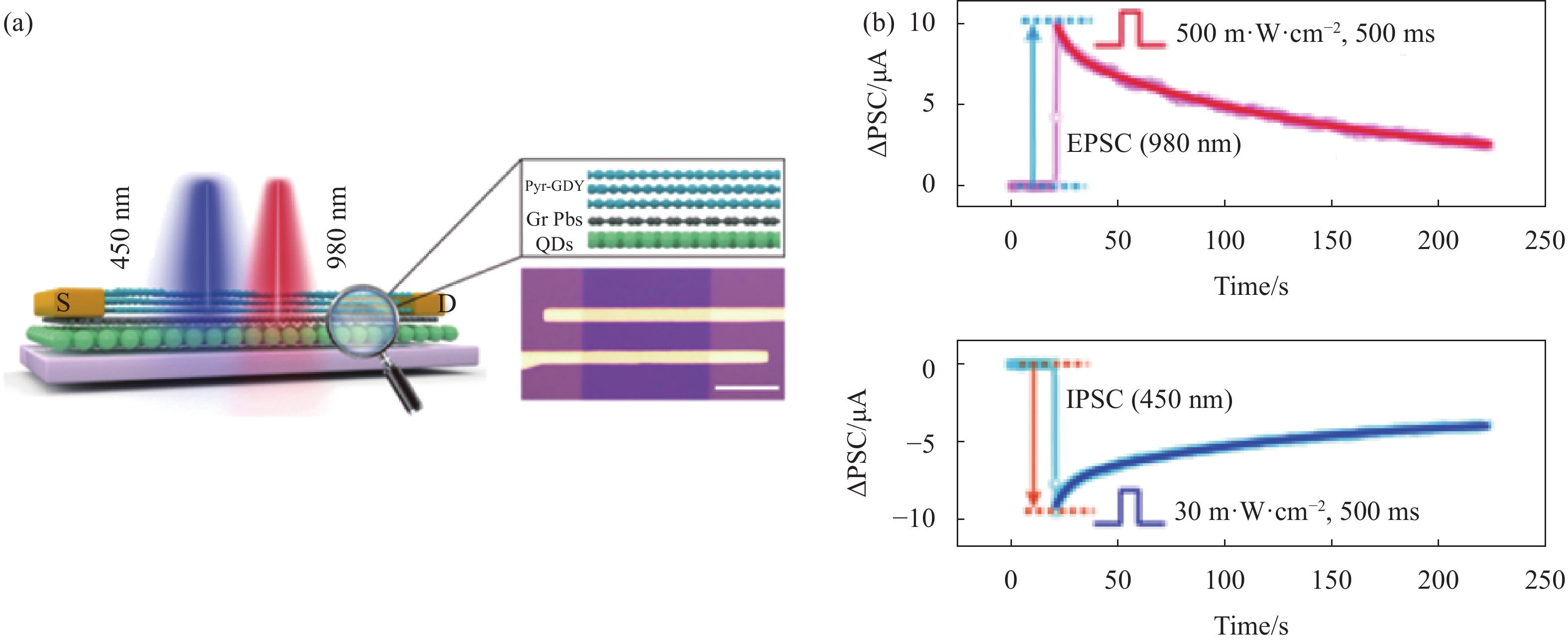
传统的冯诺伊曼架构计算机的运算单元与存储单元是物理分离的,在处理信息的过程中必然会有大量数据在运算单元与存储单元之间传输,导致高能耗并且限制了其效率。人脑却可以低能耗、高效率的处理各种复杂的并行任务,因此类脑计算被科研人员广泛关注。人脑中突触作为构成神经网络的基本单元,其同时具备着信息存储与信息处理的功能,因此利用电子设备来模拟生物突触是迈向类脑计算至关重要的一步。其中,光子突触兼具光敏性与突触功能,具有提升信息处理速度和降低能耗的优势,是目前研究的新方向。局域场增强石墨烯光电探测器优秀的光电探测能力为光子突触提供了一个崭新的平台。2020年,Yaxin Hou等提出了一种基于Pyr-GDY/Gr/PbS-QDs三层异质结构的全光调控突触器件[22],器件结构如图5(a)所示。该器件将石墨烯夹在异质结中间,基于上下两个方向相反的内在电场,利用450 nm和980 nm两个波段产生了双向响应,成功的模拟了生物突触的EPSC和IPSC行为(图5(b))。并利用基于器件的电导率变化曲线构造了一个三层人工神经网络,实现了带噪声的手写数字的模式识别。此外,由于石墨烯出色的机械性能,成功制备了柔性的光子突触,器件在多次弯曲折叠后性能衰减微弱。该工作为设计全光调控的光子突触提供了一种思路,并且简单的异质结构也为设计石墨烯柔性可穿戴光子突触提供了一个有效的策略。

Figure 5. Graphene heterojunction device with all-optically modulated photonic synapses function. (a) Device heterostructure diagram of the photonic synapse;(b) EPSC and IPSC of the device triggered by an optical pulse with wavelengths of 980 and 450 nm, respectively[22]
-
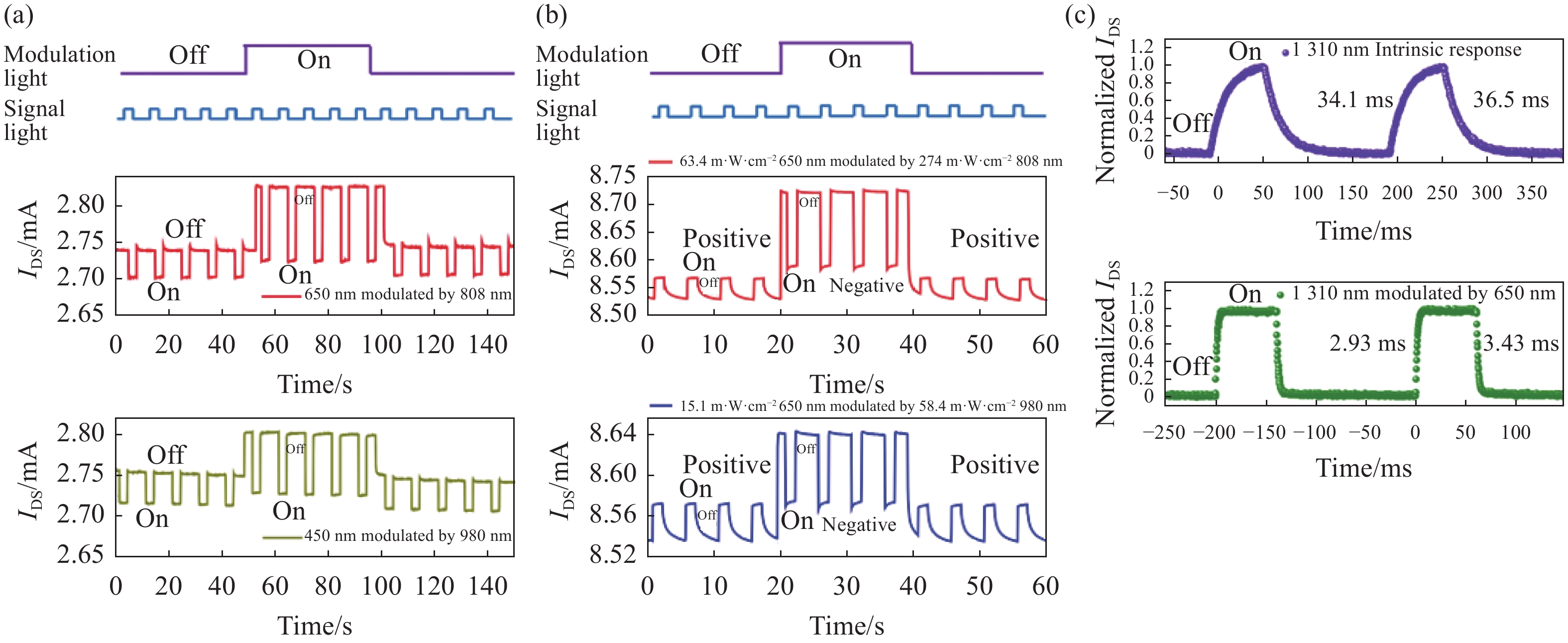
光电设备的光信号状态可以被外部信号所调制改变,通常通过栅极电压来调节光信号的幅度、速度等,如能通过外部光信号对器件的本征光信息进行调制可以简化系统的电路复杂度以及降低能耗,因此研究光调制的光电器件对发展光逻辑、光通信等领域至关重要。石墨烯结合双层异质结构具有独特的光生载流子输运行为,其为设计光调制器件提供了一个平台。2020年,Jun Wang等通过在石墨烯上制备C60/并五苯双层异质结,通过调整C60的厚度实现了多种光调制现象[23]。当C60的厚度为5 nm时,可见光产生的负响应被近红外光调制增强了2~3倍,光电流变化如图6(a)所示。增加C60的厚度至11 nm时,可见光产生的正响应被近红外光调制后,其极性发生了反转,光电流的变化如图6(b)所示。并且,近红外光下的正响应被可见光调制后,响应速度明显变快,其变化过程如图6(c)所示。该器件在可见光和近红外光波段的相互调制现象为研究异质结之间的电荷转移提供了基础,该工作为发展光逻辑以及多功能光电设备提供了一种有效的方案。
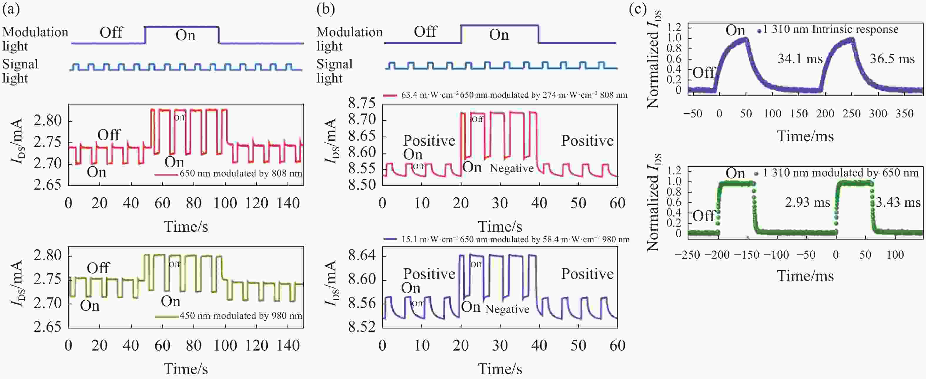
Figure 6. Visible and near infrared bidirectional light modulation. (a) Variation of photocurrent of visible Light under Near-infrared Modulation (5 nm C60 device)[23]; (b) Variation of photocurrent of visible Light under Near-infrared Modulation (11.2 nm C60 device)[23]; (c) Change of response speed of Near-infrared Light under visible light modulation (11.2 nm C60 device)[23]
-
文中简要概括了局域场增强型石墨烯近红外光电探测器的一些最新研究成果及其功能扩展。这些工作主要依赖于光栅局域场调控二维石墨烯载流子浓度,赋予其出色的近红外光探测能力。传统的单层材料局域场调控器件因石墨烯与材料界面处能量损耗,限制了光生载流子的分离效率,导致相对较差的量子效率以及相对较长的响应时间。而平面异质结局域场提供了一个垂直方向的光生载流子分离电场,促进了光生载流子的解离,并且响应时间提高到了微秒级别。然而,平面异质结的光生载流子分离只限于结区附近,这使大部分光能没有被充分利用。基于此,体异质结局域场调控被引入有效克服了平面异质结有限的光电转换效率,使局域场增强型石墨烯近红外光电探测器的灵敏度可与工业上的硅光电探测器相媲美。
然而,目前局域场增强型石墨烯光电探测器的研究大多数集中在可见光和近红外波段,在中远红外波段的探测性能普遍较低。提升探测器在中远红外乃至太赫兹波段的探测性能对于未来其应用于军民等领域是至关重要的。目前,限制局域场增强型石墨烯探测器中远红外光电探测性能的重要原因是长波材料的半导体能带较窄,难以通过局域场有效的提取其光生载流子。因此,考虑如何避免长波激发的光生载流子复合和长波辐射的背景噪声影响,并将光生载流子有效提取到石墨烯通道中,对下一步提升局域场增强型中长波红外光电探测器非常重要。
另一方面,随着人工智能、万物互联时代的到来,迫切需要可以集成多种功能的光电系统。而局域场增强型石墨烯光电探测器在光逻辑、光通信、光存储、机器视觉、神经计算等领域的性能已被探索,并且其能够制备在柔性衬底,可以实现大面积图形化加工,因此多种功能集成的局域场增强型石墨烯光电器件也会备受关注。
Localized field enhanced graphene-based near-infrared photodetector (Invited)
doi: 10.3788/IRLA20210823
- Received Date: 2021-10-10
- Rev Recd Date: 2021-12-25
- Available Online: 2022-02-10
- Publish Date: 2022-01-31
Fund Project:
National Natural Science Foundation of China (61922022,62175026)
-
Key words:
- infrared photodetector /
- localized field /
- photogating effect /
- graphene
Abstract: Near-infrared photodetectors are widely used in night vision, biomedical, environmental monitoring and many other fields. Two-dimensional graphene have great potential in infrared detection due to their unique properties (Zero band gap structure, high carrier mobility, adjustable work function). In order to take full advantage of graphene and overcome its disadvantages of low absorption and high noise, the researchers designed the hybrid structure using localized modulation of grating to improve the infrared detector performance. The research results of localized field enhanced graphene-based near-infrared photodetector were summarized, the localized field enhanced devices with single absorption layer was introduced, and the advantages and disadvantages of devices based on different types of photosensitive materials were analyzed. The double absorption layer local field enhanced device was further introduced, and the current polarity and other related researches of the research group in the field of double absorption layer devices was summarized. Finally, the research on the extension of the localized field enhanced detector was introduced, and the development trend of this kind of devices was briefly summarized and prospected.


 DownLoad: