


-
近几年随着自动驾驶的热潮兴起,对激光雷达的要求也越来越高,随之,高功率高可靠性的激光雷达光源也引起了越来越多的关注。半导体激光器有成本低,体积小,可靠性高,系统简单,利于集成等优点成为最佳的光源选择。其中最适用的光源主要有1550 nm和905 nm两个波段,前者是人眼安全波段,但是探测器成本过高限制了发展;后者适用更便宜的硅探测器,在水汽和复杂大气环境的损耗较小,传输距离远[1]。并且利用隧道结技术在材料外延生长过程中直接将多个激光器外延层串联,可以在更小的空间内集成多个激光器,在提高输出功率方面有极大的优越性。综合性能和成本考虑,905 nm高功率脉冲隧道结级联半导体激光器现已广泛用于激光测距、三维测绘等领域[2-3]。
为了实现激光雷达更远的探测距离和更佳的探测精度,半导体激光器需要更高的峰值功率和更小的发散角。2010年,Vinokurov等人报道了一种MOCVD生长的三有源区9 xx隧道级联激光器,在100 ns脉冲宽度、1 kHz重复频率、90 A脉冲条件下,输出功率250 W,斜率效率3 W/A[4];2018年,侯继达等报道了一种非对称大光腔波导的三有源区隧道级联激光器,在100 μm发光区宽度、150 ns脉宽、6.67 kHz重复频率下,输出峰值功率122 W,斜率效率3.54 W/A,垂直方向的半高全宽27.6° [5];2019年,Yuzhen Qiu等报道了一种四有源区隧道结半导体激光器,在284 μm条宽、200 ns、5 kHz的条件下,35 A达到了150 W的峰值功率,斜率效率4.66 W/A,垂直方向远场发散角29.7°[6]。高脉冲电流工作下,由于 P型波导的低迁移率,高偏压下的能带弯曲引起的载流子泄漏导致了激光器功率下降[7-10]和远场发散角较大依然是目前亟待解决的问题。
文中基于InGaAs/AlGaAs材料体系、双量子阱、以及非对称大光腔结构探究了波导结构对905 nm隧道级联半导体激光器的光束质量和功率效率的影响,提出一种非对称大光腔的波导结构,并通过优化掺杂实现了低电阻与高斜率效率的平衡,这种905 nm四有源区隧道级联半导体激光器在腔长800 μm、发光区宽度200 μm、25 ℃、100 ns脉冲宽度、1 kHz重复频率的条件下达到了斜率效率4.7 W/A,峰值输出功率177 W,垂直方向远场发散角24.3°。
-
半导体激光器的功率效率主要体现在I-V特性和I-P输出特性上,要提升半导体激光器的功率效率主要有两个方面,一是减小体电阻,降低电压损耗;其次是提升斜率效率。为了降低电阻,需要P型波导掺杂浓度比N型波导高,但其载流子为空穴,迁移率却较N面电子低得多;同时,P型波导空穴的吸收截面系数远高于N型波导电子的吸收截面系数,造成了严重的自由载流子吸收损耗[11-12]。
相比于对称的波导结构,在波导厚度不变的情况下N型波导厚,P型波导薄的非对称波导结构将会有效降低体电阻,降低载流子吸收损耗,有效提高半导体激光器的功率和效率。但是随着量子阱向P面移动,量子阱与基模光场逐渐错开,导致基模的光限制因子降低,同时高阶模式的光限制因子逐渐增加,会导致高阶模激射,光束质量降低。然而,实际的波导中增益区平均折射率高于波导层,有利于限制基模。因此,可以通过改变增益区的折射率和厚度来调整平均折射率,达到限制基模的目的。
基于以上论述,文中使用Pics3 D软件,模拟了单PN结下不同增益区类型,不同P波导(WG)厚度的波导结构对不同模式的限制因子,阈值材料增益和斜率效率的影响。如图1所示,文中基础波导设计采用大光腔结构,量子阱采用InGaAs材料,波导总厚度为2 μm;限制层(cladding)采用高Al组分AlGaAs材料,提高带隙宽度,增强载流子限制能力[13],提高大电流下的输出能力。另外,提出三种不同的增益区类型,其中,a型增益区为双量子阱单势垒(barrier)结构;b型增益区为双量子阱三势垒结构;c型增益区在b的基础上增厚了N面势垒;其中相对于波导,高折射率的增益区厚度c>b>a。

Figure 1. Schematic diagram of basic waveguide structure. a, Double quantμm well single barrier structure; b, Double quantμm well three barriers structure; c, Double quantμm well three barriers, thickening N-side barrier
基于以上三种不同增益区类型,模拟了不同波导结构对基模与高阶模的阈值增益的影响,从而找到合适的波导结构能有效抑制高阶模输出,改善光束质量,在减小腔内模式竞争的同时提升激光器的输出功率、 斜率效率及电光转换效率。阈值材料增益如公式(1)所示:
式中:Gth为阈值材料增益;αi为内损耗;(1/L)ln(1/R)为腔面损耗;Г为限制因子。
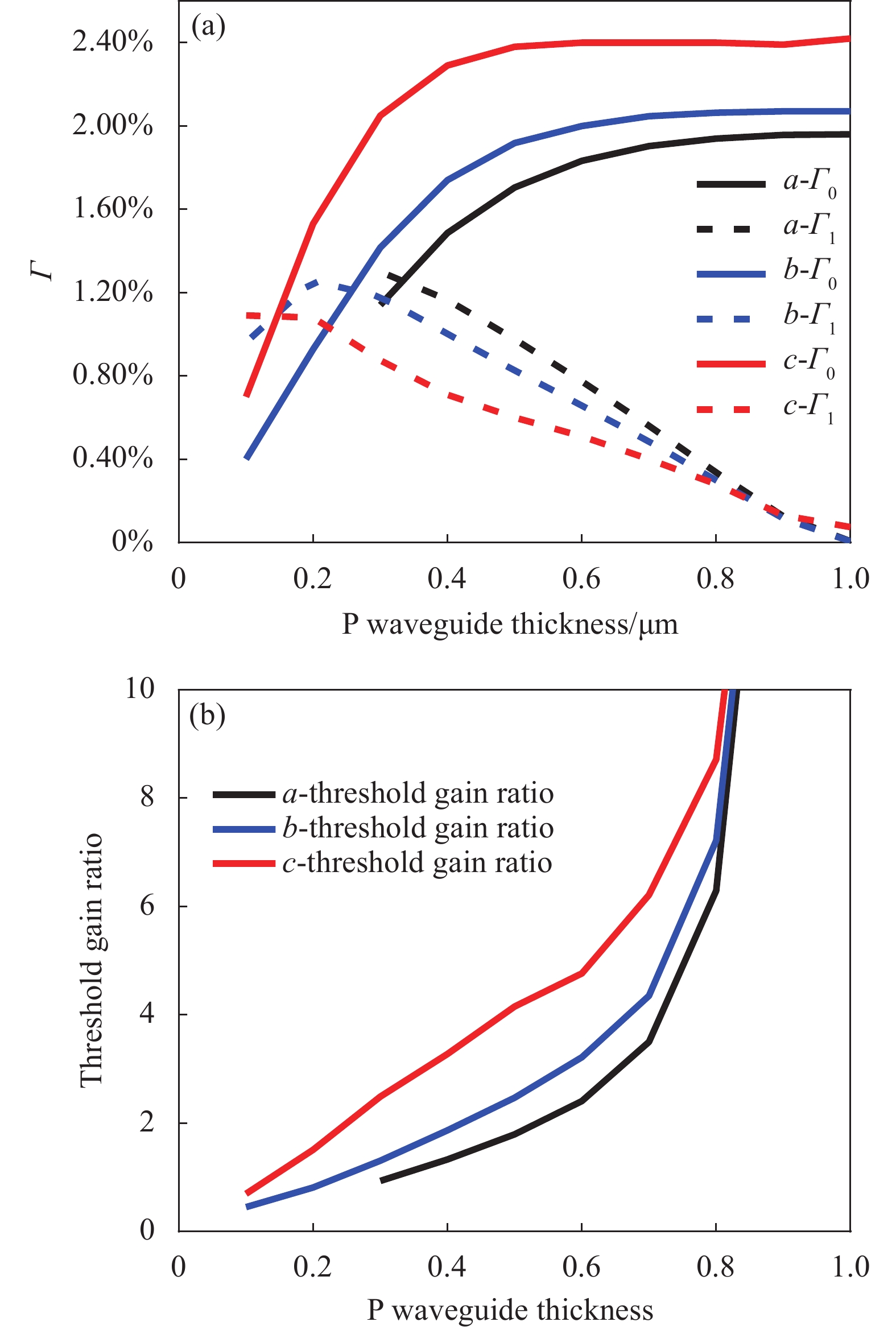
模拟了三种增益区类型,不同波导结构对限制因子的影响,如图2(a)所示,三种不同增益区类型的波导结构随P型波导厚度减小,都是呈基模限制因子减小,一阶模限制因子增大的趋势。在P面波导厚度相同时,基模限制因子c>b>a;一阶模限制因子a>b>c。笔者定义一阶模阈值材料增益对基模阈值材料增益的比值为阈值增益比(后文简称为阈值增益比)。三种增益区类型,不同波导结构对阈值增益比的影响如图2(b)所示。

Figure 2. (a) Effect of different waveguide structures on the limiting factor; (b) Effect of different waveguide structures on the threshold gain ratio
阈值增益比越大,高阶模越不容易达到激射条件,这时可以得到更好的抑制。在阈值增益比较大时,基模占主导因素,高阶模被抑制;在阈值增益比较小时,基模与高阶模都有可能增益饱和产生激射,基模与高阶模光斑耦合,甚至完全使高阶模激射,产生光斑“多瓣”现象,光束质量劣化。随着P型波导厚度减小,阈值增益比总体呈下降趋势,其中c增益区类型下降最缓,a增益区类型下降最快。
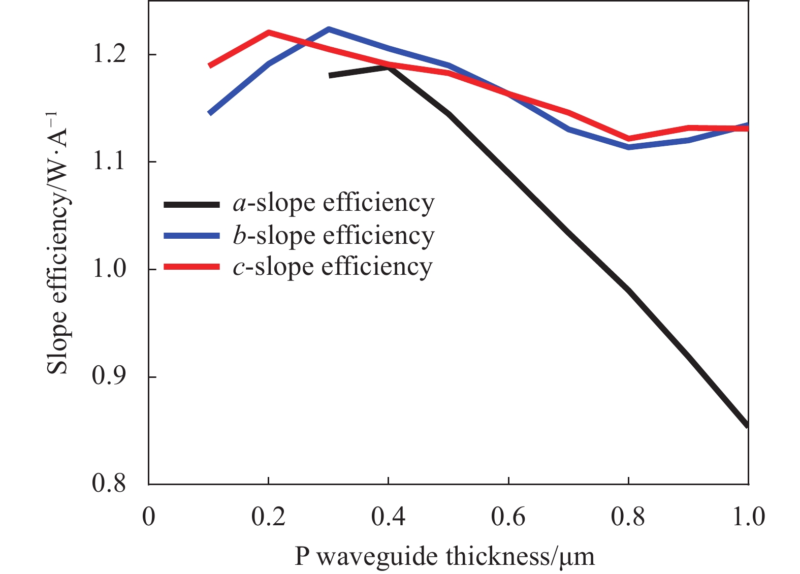
针对三种增益区类型,模拟得出了不同P型波导厚度的波导结构对斜率效率的影响,如图3所示。a增益区类型在P面波导厚度较大时,其载流子限制能力弱,斜率效率很低,随着P型波导厚度减小,其斜率效率逐渐增大,在P型波导厚度0.4 μm左右达到最大值。波导结构b和波导结构c的斜率随N面波导增加呈曲折变化,且在P型波导厚度为0.3 μm和0.2 μm左右有极大值。
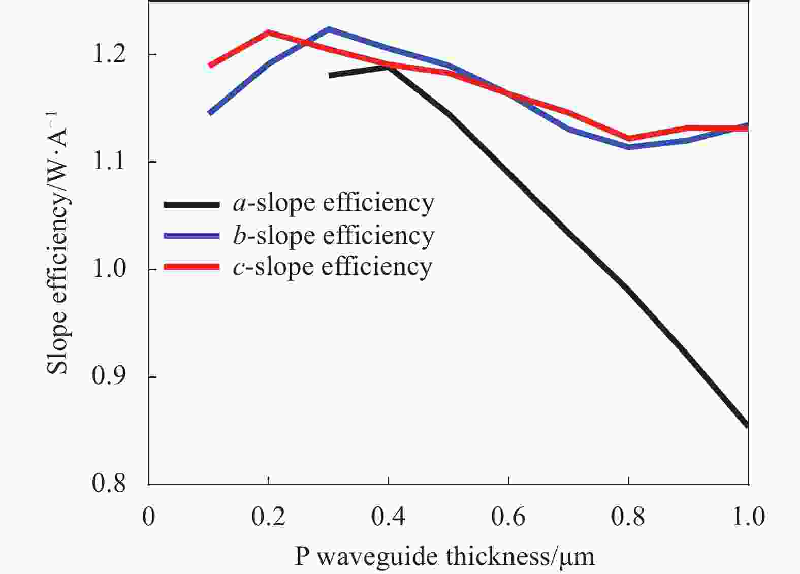
Figure 3. Effect of different waveguide structures on slope efficiency
结合不同增益区类型随P型波导厚度减小的波导结构对模式限制与斜率效率的影响,综合考虑取以下几组不同波导结构的条件设计了三有源区和四有源区的激光器外延结构,部分参数见表1。
-
根据表1中所示的结构,笔者进行了外延生长,流片和测试表征。首先利用金属有机化学气相沉积(MOCVD)进行了905 nm多有源区半导体激光器的外延生长,隧道结处的外延生长需要重掺杂的GaAs以减小电阻和作为多个有源区的隧穿路径[14]。
Number Gain region type P-WG thickness/μm Barrier thickness /μm Fundamental mode Г Bulk resistance/Ω Threshold gain ratio A1 a 0.75 0.01 1.69% 0.22 4.5 A2 a 0.45 0.01 1.31% 0.21 1.2 A3 a 0.35 0.01 1.04% 0.205 0.9 B b 0.35 0.03 1.59% 0.18 1.6 C c 0.25 0.07 1.58% 0.18 2 Table 1. Device preparation parameters
外延生长后进行激光器的波导结构刻蚀和电极制备。由于重掺杂的隧道结和有源区之间激光器的注入电流会产生严重的横向扩展。为了抑制电流扩展,采用深腐蚀沟槽结构,刻蚀深度超过接近衬底一侧的有源区量子阱,在三有源区和四有源区的隧道结级联激光器中,刻蚀深度均超过12 μm。沉积300 nm厚的SiO2作为绝缘层,然后光刻形成200 μm宽的电极窗口,蒸镀Ti-Pt-Au和电镀金作为P面电极,然后背面减薄至150 μm左右,并溅射N面电极金属。接着将晶圆解理为800 μm腔长的巴条,进行腔面钝化,后腔面镀99%以上的高反射膜,前腔面镀15%反射率的增透膜。最后解理为400 μm宽的单管芯片,P面朝上封装在TO管壳上用作后续的测试。
测试使用的条件都是100 ns脉冲宽度,1 kHz的重复频率,脉冲测试系统是基于LSP-40脉冲模块,这个模块脉冲宽度在50~1000 ns之间可调,输出电流在0~41.6 A之间。功率采集使用高灵敏度的功率计(型号为PowerMax PM150)采集平均功率,然后通过占空比计算峰值功率。远场的测试是用CCD采集在41.6 A的脉冲电流工作下的输出图像,然后用Matlab对采集到的图像进行垂直方向的扫描,得到光强分布随角度变化的远场发散角。
笔者对A1、A2、A3三个结构进行了PIV(图4(a))和垂直方向远场发散角(图4(b))的测试,结果如图4所示。随着P面波导厚度减小,体电阻减小,阈值增益比也随之减小。A1结构的激光器,在25 ℃、100 ns、1 kHz的条件,41.6 A的驱动电流下A1、A2、A3峰值功率分别为107 W、125 W和118 W。并且在低电流情况下,三种结构的斜率效率基本一致,在电流大于15 A以后呈现不同程度的功率饱和现象,并且峰值功率A2>A3>A1,表明不同的波导结构对载流子泄露引起的功率饱和有影响。

Figure 4. (a) PIV curves of triple-active regions semiconductor lasers with waveguide of A1 (red), A2 (green), A3 (blue); (b) Far field divergence angles of triple-active regions semiconductor lasers with waveguides of A1 (red), A2 (green), A3 (blue) in the vertical direction
可以看出,A1、A2、A3三个结构的阈值增益比分别为4.5,1.2和0.9。在阈值增益比为4.5时,激光器垂直方向单模激射,输出光斑为基模(文中只讨论垂直于PN结方向的激光模式,后文所述基模,单模和高阶模为垂直于PN结方向的基模,单模与高阶模式),其垂直方向远场发散角半高全宽(Full width at half maximum,FWHM)为26.8°。在阈值增益比等于1.2时,激光器对高阶模式的限制能力减弱,有高阶模的激射,远场输出光斑呈双峰,表现为基模与一阶模的叠加,其FWHM急剧上升,为57.5°。随着阈值增益比进一步减小,当阈值增益比等于0.9时,激光器高阶模式激射,输出光斑呈双峰,表现为完全一阶模,其FWHM继续增加至59.2°。随着阈值增益比减小,激光器不能维持基模工作,高阶模的成分逐渐增加。
笔者对增加势垒数量的B结构激光器进行表征,如图5所示,B波导结构的激光器具有和A3相同的P面波导厚度,在25 ℃、100 ns、1 kHz的条件下,41.6 A的峰值功率提高到132 W,且未出现明显的功率饱和。说明相比A型波导,B型波导结构增加了两个势垒结构,增加了限制载流子泄露的能力,提高了高脉冲电流下的峰值功率。但是其FWHM为30.1°,远场发散角比模拟值大很多,表明一阶模有部分激射,导致远场发散角增大。说明1.6的阈值增益比仍有高阶模部分激射的风险,需要进一步增大阈值增益比。
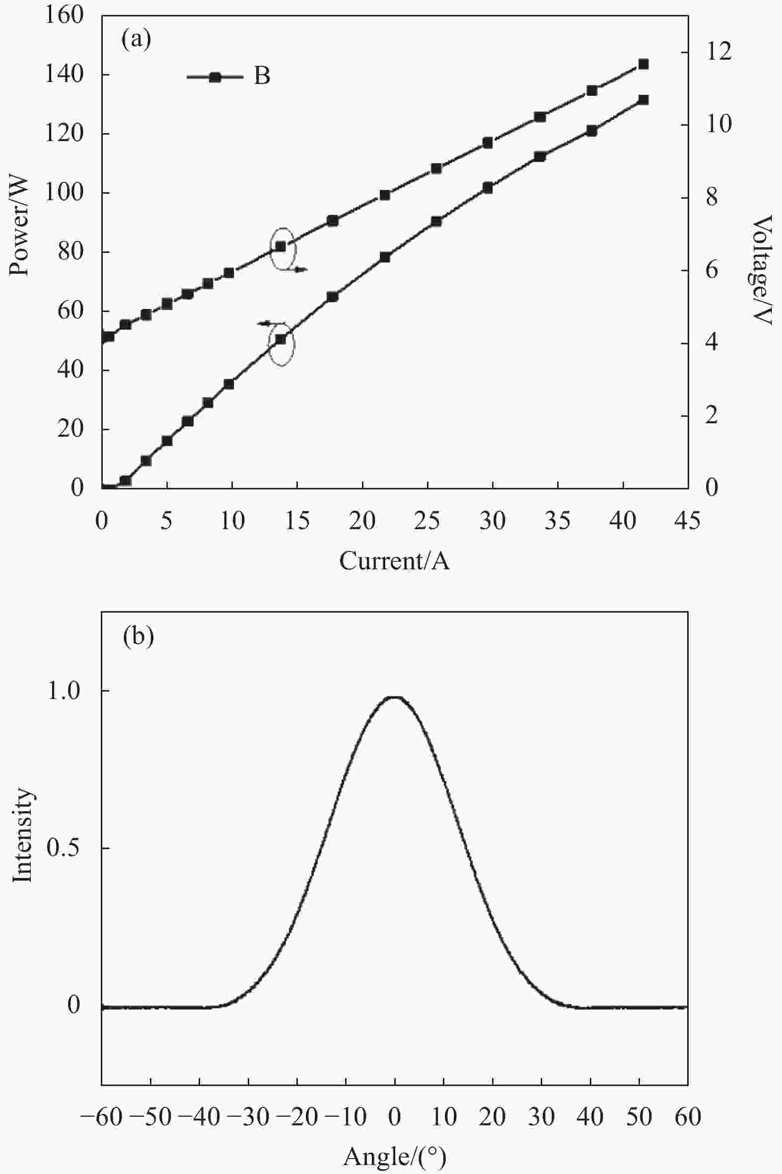
Figure 5. (a) PIV curve of triple-active regions semiconductor laser with B waveguide structure; (b) Divergence angle of far field in vertical direction of triple-active regions semiconductor laser with B waveguide structure
如图6所示,在B波导结构的基础上,为了进一步优化输出性能,使用了C波导结构,对N面势垒增厚至50 nm,提高了基模限制因子。 C波导结构的激光器,在25 ℃、100 ns、1 kHz的条件下,41.6 A的峰值功率三有源区和四有源区分别达到了133 W和177 W。C波导结构的激光器的阈值增益比等于2,三有源区和四有源区FWHM分别为24.1°和24.3°,与模拟值24.7°接近,说明是基模激射。三有源区的C结构达到了和B结构相当的峰值功率,且高阶模得到了完全抑制,实现了垂直于PN结方向的单模工作,远场发散角有较大的优化。

Figure 6. (a) PIV curves of semiconductor lasers in the triple-active regions (black)and quadruple-active regions (red) with C waveguide structure; (b) Far field divergence angles of semiconductor lasers in the triple -active regions (black) and quadruple-active regions (red) with C waveguide structure
综合以上个三结构,笔者发现激光器的发散角与阈值增益比有强相关性。如图7所示,将不同阈值增益比的激光器41.6 A的实测发散角和模拟的基模发散角进行对比。可以看出,当阈值增益比大于等于2 时,激光器的实测发散角与模拟的基模发散角很好地吻合。但当阈值增益比小于等于1.6时,实测的发散角大于模拟值,说明高阶模式已经开始工作,且随阈值增益比的降低,高阶模式的成分逐渐增加。根据实验数据的分析,笔者总结存在支持多个模式的大光腔波导结构中,阈值增益比大于等于2的非对称大光腔波导结构可以实现基模工作。
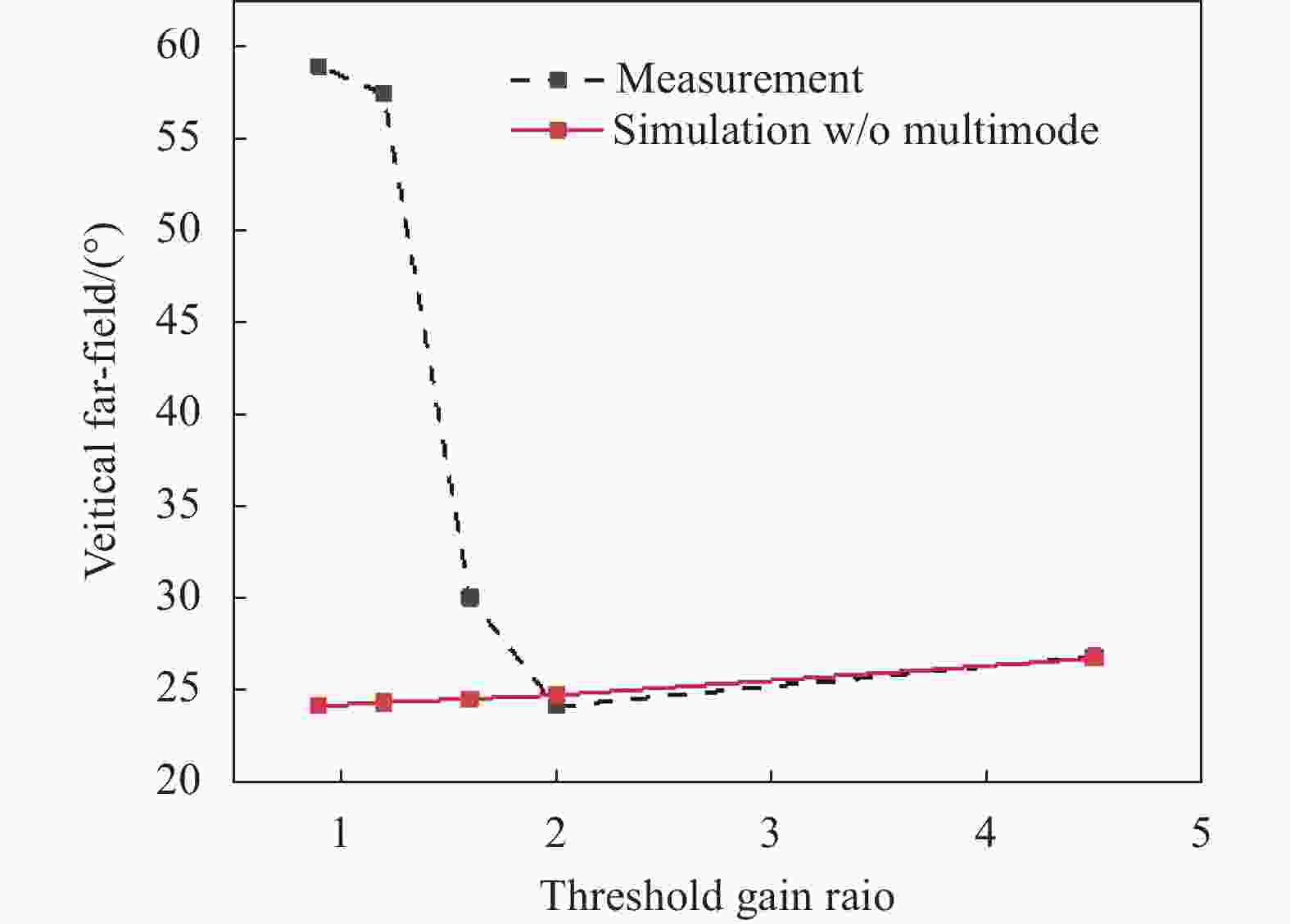
Figure 7. Variation trend of far-field divergence angle of semiconductor lasers with riple-active regions under different threshold gain ratios; measured (black), simulated (red)
不同的增益区类型、不同波导结构的器件输出性能表明:相对折射率高的势垒层和更窄的P面波导有利于限制载流子泄露及降低载流子泄露导致的功率饱和现象,使得在高脉冲电流工作的情况下,器件有更高的峰值功率;同时更窄的P面波导能有效降低体电阻,这两点共同提高了器件的输出效率。但是,P面波导厚度减小时限制因子和阈值增益比也同时减小,有高阶模式激射的风险。因此,在波导结构的设计中应该在保证垂直于PN结方向单模工作时(阈值增益比大于等于2)尽量降低P面波导厚度。
-
文中通过对不同波导结构的限制因子和阈值增益比以及斜率效率的模拟分析,研制并测试比较了几组不同量子阱类型、不同波导结构的激光器,发现具有更厚的N面势垒、更窄的P面波导结构的激光器对载流子限制能力更强,有更高的峰值输出功率;并且在阈值增益比大于等于2的时候,激光器能够在垂直于PN结方向单模工作。基于这些研究,设计并研制了0.8 mm腔长、200 μm条宽的四有源区大功率905 nm半导体激光器。在25 ℃、100 ns脉冲宽度、1 kHz重复频率的条件下,41.6 A工作电流下的峰值功率达到了177 W,其垂直方向远场发散角为24.3°。实验结果与模拟设计具有良好的一致性,为非对称大光腔波导结构的功率效率与远场发散角的设计提供了理论指导。
Effect of waveguide structure on beam quality and power of 905 nm cascade semiconductor lasers with tunnel junctions
doi: 10.3788/IRLA20210979
- Received Date: 2021-12-17
- Rev Recd Date: 2022-02-22
- Accepted Date: 2022-03-03
- Publish Date: 2022-06-08
-
Key words:
- waveguide structure /
- semiconductor laser /
- tunnel junction cascade /
- beam quality /
- power optimization
Abstract: In recent years, lidar applications had put forward higher requirements for detection distance and sensitivity. As an ideal light source, 905 nm semiconductor lasers also urgently needed to improve the peak power and beam quality. In this context, the effects of different gain region types and waveguide structures on beam quality and power efficiency of 905 nm tunnel-junction pulsed semiconductor lasers were investigated based on asymmetric large optical cavity structures. By optimizing the gain region type and waveguide structure, the bulk resistance and internal loss were reduced. The ability to limit carrier leakage was enhanced, and the peak power and electro-optical efficiency of the device working at high currents were improved. By increasing the threshold gain ratio of the multimode to the fundamental mode, the high-order mode lasing was suppressed, and the far-field divergence angle was reduced. On this basis, the developed quadruple-active regions semiconductor laser with 800 μm cavity length and 200 μm electrode achieved a peak power output of 177 W at a pulse current intensity of 41.6 A in pulse power test with a pulse width of 100 ns and a repetition rate of 1 kHz; fundamental mode emitting in the vertical direction, the full width at half maximμm far-field divergence angle was 24.3°.


 DownLoad: