


-
红外探测器利用物体本身各部分温度辐射与发射率的差异获得目标细节,并通过光电转换、电信号处理等手段将目标物体的温度分布显示为人眼可见的图像。由于焦平面红外探测器具有抗干扰能力强、隐蔽性好、获取的场景信息丰富等优点,因此在导航、制导、监控、预警、工业检测和医疗卫生等领域均具有广泛的应用。
焦平面红外探测器的数字读出是其发展的一个重要方向。相比传统的模拟红外焦平面探测器,数字红外焦平面探测器具有抗干扰性强、传输带宽高以及稳定性好等优点。数字红外焦平面技术的核心在于数字读出电路(Digital readout integrated circuit, DROIC)技术,其通过将模拟-数字转换器(ADC)集成进读出电路中,使得探测器光电流信号在片内实现数字化,读出电路直接输出数字信号,是下一代红外焦平面探测器的通用基础技术[1]。
为了获得更高的空间分辨率,或通过单个探测器获得更大的视场(FOV),目前焦平面红外探测器正朝着大面阵、小像元尺寸的方向发展,这对数字读出电路的设计提出了诸多挑战,例如小面积读出单元电路设计、小面积ADC设计、以及高速数据传输电路设计等,以上设计都必须以低功耗实现,以降低制冷机的功耗、体积和成本等[2]。文中首先介绍了数字读出电路技术的发展现状,然后详细介绍了用于短波红外焦平面红外探测器的1280 × 1024,10 μm的数字读出电路设计,最后给出了测试结果以及与探测器完成倒装焊互连后的组件的成像效果。
-
国际上,在数字读出电路技术上领先的机构主要有以色列的SCD公司、美国的Lockheed Martin公司(以下简称洛马公司)以及法国的Lynred公司等。由于读出电路通常针对特定红外焦平面探测器进行设计,只有少数公司将其作为独立的产品,所以这里通过介绍数字焦平面红外探测器的发展现状来阐述数字读出电路的技术水平。
以色列的SCD公司是最早启动数字读出电路研究工作的公司之一,早在2011年就推出了面阵规格为640 × 512,像元中心距为15 μm的数字探测器组件,其产品代号为Pelican-D;之后SCD公司在此基础上进行了技术提升,推出了Hercules系列产品,面阵规格扩大为1280×1024;2017年,SCD公司推出10 μm像元中心距的新产品系列BlackBird,面阵规格覆盖了1920 × 1536、1280 × 1024和640 × 512,成为世界领先的数字红外成像组件供应商[3]。洛马公司下属的Santa Barbara Focal plane公司是全球领先的红外焦平面探测器生产厂商,其产品线齐全,面阵规格覆盖了320 × 256 ~ 2560 × 2 048,其中SBF234和SBF259均为1280 × 1024面阵规格,8 μm像元中心距的产品,而SBF246更是实现了2 048 × 2 048的面阵规格,像元中心距同为8 μm[4]。法国的Sofradir曾是世界领先的红外焦平面探测器厂商,2019年与ULIS进行重组后成为现在的Lynred公司,其旗下的DAPHNIS-HD和DAPHNIS-XGA产品达到了1280 × 720和1024 × 768的面阵规格,像元中心距达到了10 μm [5]。
“十二五”期间国内各大研究机构已经开展了数字红外焦平面读出电路及数字探测器的研究工作。昆明物理研究所经过多年的技术攻关,现已取得了一定的成果,2015和2019年先后发布了640 × 512,15 μm的中波及短波两款数字红外焦平面探测器组件[1, 6],并于2021年发布了384 × 288,25 μm的长波数字焦平面探测器组件,该组件采用最新的数字像元技术和数字积分技术,动态范围达到95.2 dB,最高帧频可以达到1012 Hz[7]。
-
根据ADC集成进读出电路的方式不同,数字读出电路也有以下3种架构:片级、列级以及像素级ADC数字读出电路架构。其中,像素级ADC数字读出电路架构虽为目前最先进的架构[8],但是要在10 μm ×10 μm的面积内实现高分辨率ADC的设计具有较大的难度,而且131万个ADC同时工作,读出电路的功耗将十分可观,因此并不适用与1280 × 1024,10 μm的读出电路设计。相比较而言,列级ADC数字读出电路架构在各方面性能和电路实现之间具有较好的平衡,是小像元读出电路的主流架构之一。列级ADC数字读出电路架构如图1所示,整个读出电路包含读出单元电路、ADC阵列以及数据传输电路三个主要部分组成。下面对应用于短波红外焦平面探测器的数字读出电路的各组成模块设计进行介绍。

Figure 1. Diagram of the 1280 × 1024, 10 μm DROIC
-
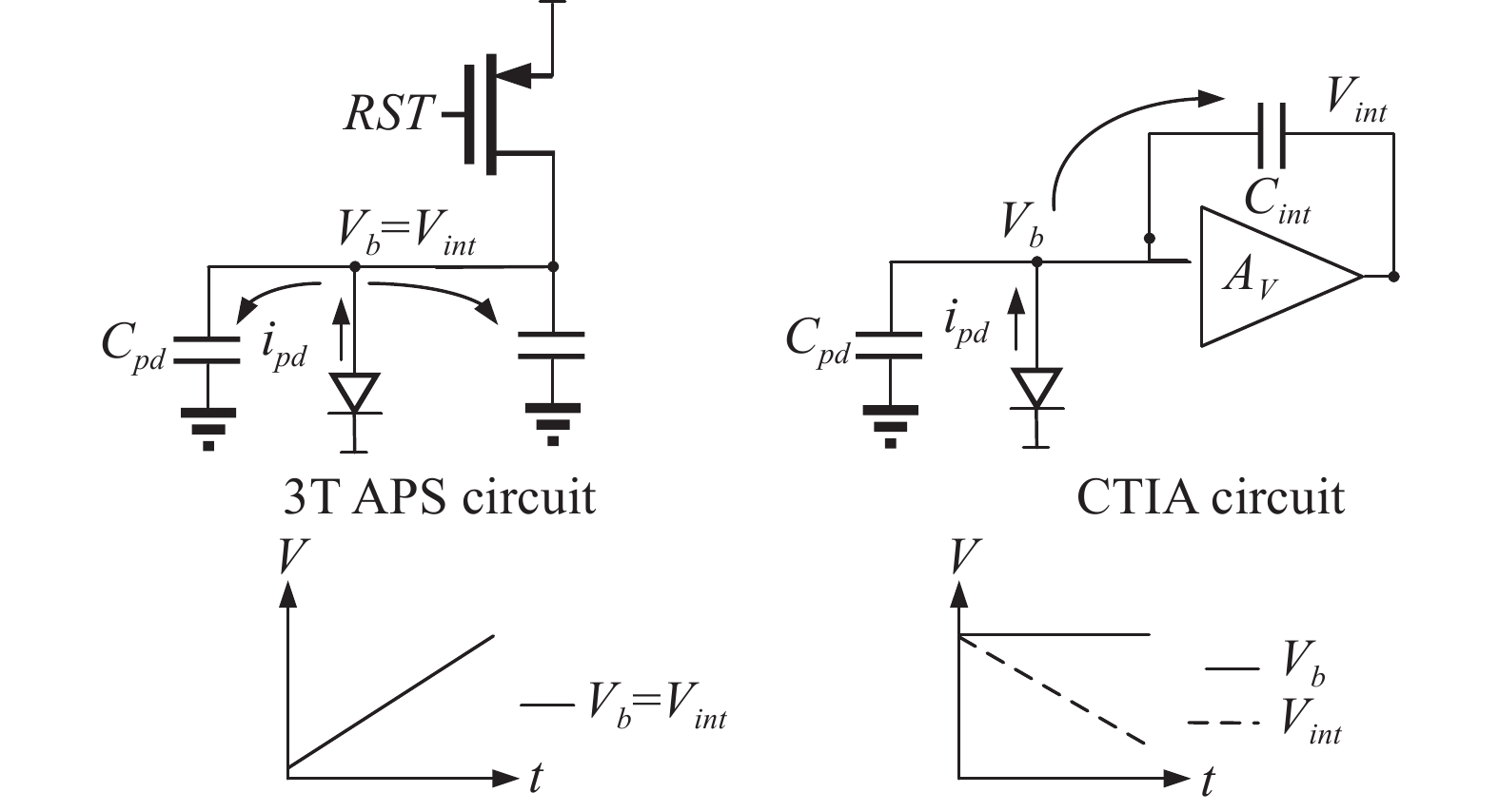
读出单元电路的功能是将探测器光电流进行积分,转换成电压信号后传输至下一级电路进行处理。短波红外探测器相比中波和长波红外探测器具有光电流较小的特点,因此需要采用高注入效率的注入级电路;此外整个读出单元电路的版图面积必须小于等于10 μm × 10 μm,因此必须充分考虑读出单元电路的版图实现。
传统的注入级电路(例如3T结构)虽然具有简单的电路结构和较小的版图面积,但并不适用于短波焦平面红外探测器,因为在积分过程中探测器的偏置电压不断变化,光电流同时对积分电容和探测器分布电容进行积分,注入效率较低。文中采用电容反馈跨阻放大器型(CTIA)注入级电路,其通过引入高增益放大器,将积分电容跨接在放大器的输入端(即探测器光电二极管的正端)和输出端,探测器正端的偏置电压恒定,探测器光电流几乎只对积分电容积分,从而实现高注入效率[9]。整个读出单元电路的原理图如图2所示,其中Cint为积分电容,Cpd为探测器的分布电容。3T和CTIA结构的积分过程对比如图3所示。

Figure 2. Schematic of readout unit circuit

Figure 3. Comparation of integrations between 3T and CTIA circuit
CTIA注入级电路的核心在于高增益放大器,其增益决定了注入效率,假设放大器的增益为AV,根据注入效率的定义和米勒等效定理可以写出:
假设Cpd为40 fF,对于60 fF的积分电容设计,可以计算得到当放大器增益大于50.5 dB时,注入效率η高于99.5%。
除此以外,CTIA电路的放大器还占据了较大的版图面积。常用的放大器结构通常包含5~9个晶体管,考虑到放大器的1/f噪声以及晶体管之间的匹配等,各晶体管不能采用最小尺寸设计,因此放大器具有较大的版图面积,这对于10 μm × 10 μm的像元面积而言具有很大影响。
考虑到以上两方面,文中采用了单端共源共栅(Cascode)放大器结构,如图2所示。整个放大器只包含4个晶体管,这为小面积读出单元电路设计打下了基础,同时放大器的增益达到了68 dB,读出电路的注入效率达到99.9%。
所设计的读出单元电路采用卷帘门曝光(Rolling shot)工作模式,其工作原理为:所有像元逐行开始积分,然后逐行结束积分并将积分后的光电信号逐行读出。与全局曝光(Global shot)相比,卷帘门曝光工作模式的读出单元电路无需采样/保持电容,为小面积设计提供了基础。
-
ADC是数字读出电路的关键组成模块,其对于读出电路乃至整个红外焦平面探测器的性能有重要影响。首先,ADC的分辨率影响着整个焦平面红外探测器的动态范围,针对红外信号高动态范围的特点,ADC的位数需要达到14 bit或以上;其次,ADC的转换速度影响着读出电路的工作速率和焦平面红外探测器的最高帧频,对于面阵规格为1280 × 1024的焦平面红外探测器,如果要求帧频高于100 Hz,则要求ADC的转换速度达到128 ksps;最后,ADC的功耗直接影响读出电路和焦平面红外探测器的功耗,对于面阵规格为1280 × 1024的数字读出电路,共包含1280个ADC,单个ADC的微小功耗提升,都将为焦平面红外探测器带来可观的功耗提升,因此ADC必须以低功耗实现。
为了满足上述要求,采用参考文献[6]中报道过的高分辨率、低功耗二阶Incremental Sigma-Delta ADC(其结构框图如图4所示),并在此基础上针对大面阵、小像元中心距读出电路的特点进行了优化。

Figure 4. Diagram of the second order Incremental Sigma-Delta modulator
对于10 μm像元中心距的读出电路,单个ADC的版图宽度必须小于等于10 μm,即便将ADC阵列分为奇偶部分,分别放置于读出电路的上下两端,单个ADC的版图宽度也必须小于等于20 μm,这使得ADC的版图呈一种狭长的极端形状,不利于ADC中较为关键的模拟电路的对称性版图设计,进而造成模拟电路中差分器件的失配,并产生失调(offset);此外,对于1280 × 1024的面阵规格,整个ADC阵列的宽度将达到12.8 mm,CMOS工艺的偏差十分显著,ADC之间存在较大的电路参数(例如晶体管的阈值电压Vth,宽度和长度等)失配,这会使各个ADC的失调存在较大的差异,从而引起焦平面红外探测器的列级固定图案噪声(FPN)。
为此,在原先的设计基础加入失调消除技术(offset cancellation)以减小ADC的失调,同时降低了焦平面红外探测器的列FPN。对于二阶Incremental Sigma-Delta ADC,调制器是其主要的模拟电路模块,而调制器的核心是两个放大器,所以本次设计在放大器的输入端加入了由开关电容组成的失调消除电路,如图5所示,其工作原理如下:

Figure 5. OTA with input stage offset cancellation circuit
在ADC开始转换之前,控制信号AZ有效,此时放大器接成单位增益负的反馈结构,假设放大器的开环增益为AV,放大器输入等效失调为VOS,则此时放大器输出端的电压VOUT为:
该电压被存储在电容COS上。在ADC转换的期间,控制信号AZ保持无效,此时正常的输入信号VIN送入到放大器,根据电荷重分配的原理可以得到此时放大器的输出信号VOUT′为:
公式(3)表明,放大器的输入等效失调电压被减小至:
对于所设计的放大器,开环增益为60 dB,因此其输入等效失调电压被减小至原来的1/1000。
在版图设计方面,为了减小由于差分晶体管失配带来的失调,采用交叉层叠的版图布局技术,将相邻两个ADC的调制器在垂直方向进行依次叠放,单个调制器的宽度限制被放宽到40 μm,从而可以充分采用共质心版图结构;此外,还在差分晶体管周围加入dummy器件以提高差分晶体管的匹配。ADC阵列的版图布局示意图如图6所示,从图中可以看到,采用该布局还使得相邻两个ADC的调制器集中在底部,而ADC的数字抽取滤波器(Decimator)仍然在Y方向平行排列,即ADC的模拟电路和数字电路在物理上分开,减小数字电路对模拟电路的干扰。

Figure 6. Floor plane of ADC array
-
对于ADC的位数为14 bit,面阵规格为1280×1024的数字焦平面红外探测器,如果帧频为50 Hz,则读出电路的数据率约为0.9 Gbps,如果帧频为100 Hz,则数据率将超过1.8 Gbps。为了满足以上设计要求,采用了两项电路技术。
首先,采用4路高速、低功耗并行/串行数据转换电路完成ADC输出数据的多路选择和传输,所采用的并行/串行数据转换电路不仅能实现500 MHz以上的工作速率而且功耗仅为数毫瓦[6]。整个ADC阵列输出的并行数据被分为4组,分别传输到对应的并行/串行数据转换电路中转换成串行。4通道数据传输电路结构框图如图7所示。
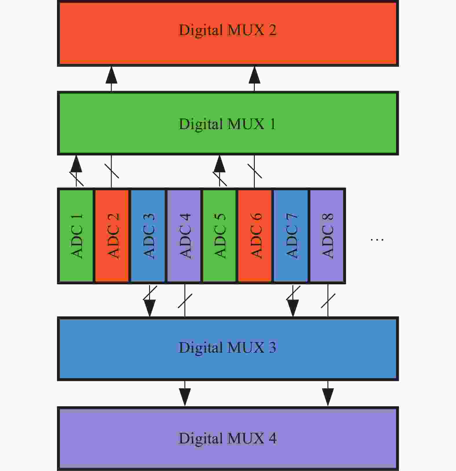
Figure 7. Diagram of 4-channel data transmission circuit
其次,采用低压差分信号(LVDS)进行数据输出。LVDS技术能实现以数Gbps的速率传输串行数据,而且具有低功耗和低误码率的特点。结合所采用的并行/串行数据转换电路单路,整个读出电路的数据率可达到2 Gbps,支持数字焦平面红外探测器最高100 Hz的帧频。
-
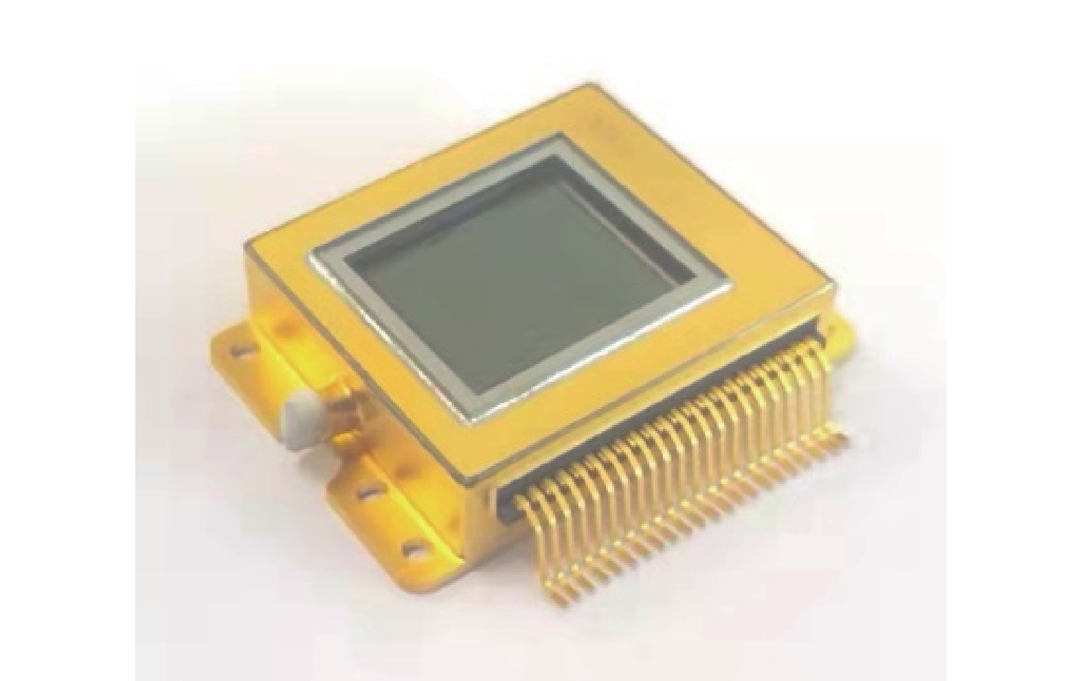
所设计的1280 × 1024, 10 μm数字焦平面读出电路基于0.18 μm标准CMOS工艺进行了实现,图8为读出电路的芯片照片,所设计的数字读出电路与短波红外探测器进行了倒装焊互连,实现了数字短波红外探测器,其照片如图9所示。基于自主开发的测试平台对所设计的读出电路进行了测试。
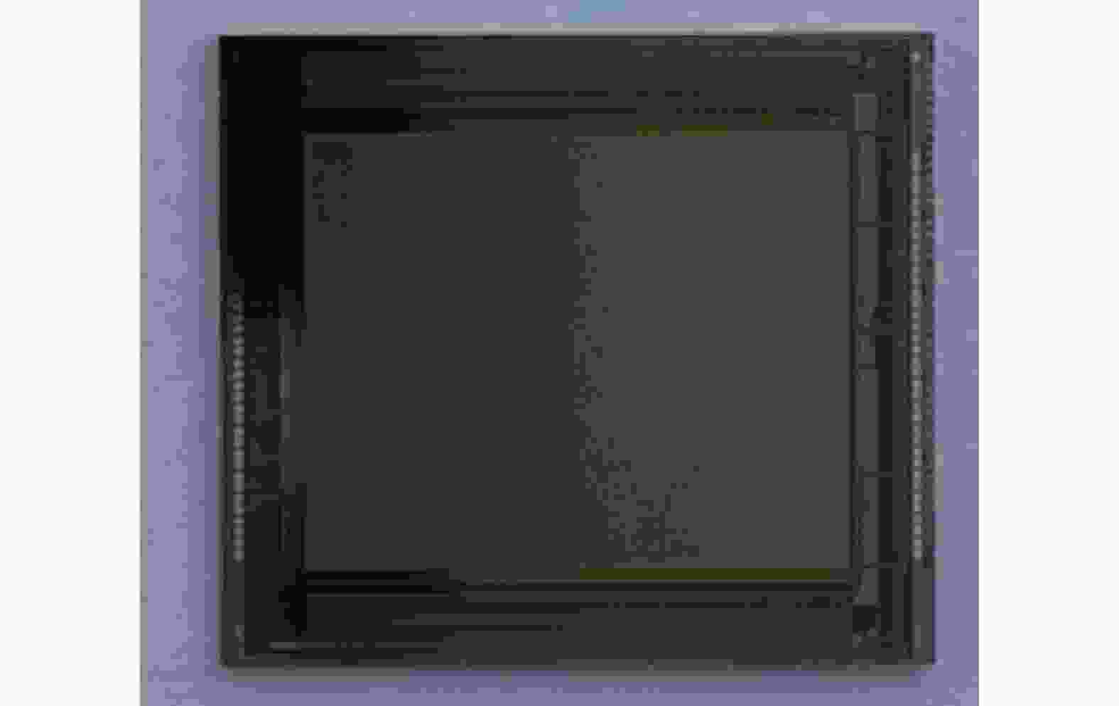
Figure 8. Picture of the proposed 1280 × 1024, 10 μm DROIC

Figure 9. Picture of the digital short-wave IRFPA
在无光电流输入的情况下,对读出电路进行200帧输出数据的采集,通过计算每个像元的RMS噪声并计算所有像元RMS噪声的平均值,最终得到整个读出电路的读出噪声为1.03 LSB(最小可分辨位数),约为157 μV,测试结果如图10所示。

Figure 10. Test result of the DROIC’s noise
同样在无光电流输入的情况下,对读出电路输出数据求各列的平均值,并计算各列平均值的RMS值,最终得到读出电路的列FPN为18.5 LSB,约为整个输出范围的0.1%。得益于对ADC阵列采用的失调消除设计,相比参考文献[6]的设计,列FPN改善了约60%,测试结果如图11所示。

Figure 11. (a) Proposed 1280 × 1024, 10 μm DROIC’s column FPN test result; (b) Column FPN test result of 640 × 512, 15 μm DROIC mentioned in Ref. [6]
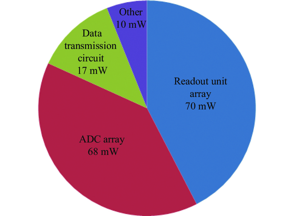
在50 Hz帧频的条件下,对读出电路的功耗进行了测试,其工作电压为3.3 V(像元阵列和ADC阵列等模块的工作电压)和1.8 V(数据传输和逻辑控制电路等模块的工作电压),测得读出电路的总功耗为165 mW,其中读出单元阵列的功耗为70 mW,ADC阵列的功耗为68 mW,4通道数据传输电路的功耗为17 mW,其余电路模块(包括逻辑控制电路和偏置电流产生电路等)的功耗为10 mW,如图12所示。

Figure 12. Power consumption of the proposed DROIC’s all components
表1统计了所设计的数字读出电路的性能指标并与国外同类产品进行了比较。所设计的数字读出电路在ADC位数和噪声等性能指标方面达到国外产品的水平,但功耗和帧频还有改进的空间。ADC的转换速度是制约读出电路工作速度的关键因素之一,此外从图12可以看到,ADC阵列的功耗占整个读出电路功耗的40%以上,因此可以采用低功耗、高速列级ADC结构改善读出电路的功耗和工作速度,例如三阶Incremental Sigma-Delta ADC结构,其完成一次转换所需的时钟个数相比文中所采用的二阶Incremental Sigma-Delta ADC可以降低约3.5倍,不仅可以支持更高帧频的应用,而且数字模块的功耗可以大大降低;从图12还可以看到,读出单元阵列的功耗也是读出电路功耗的主要组成部分,因此低功耗CTIA注入级电路设计也是项目组下一步的研究方向之一。
Parameter This work SCD cardinal 1 280 HD [10] SBF262 [4] Format 1280 × 1024 1280 × 1024 1280 × 1024 Pitch/μm 10 10 16 Reading mode IWR/ITR IWR/ITR IWR/ITR ADC/bit 14 13 22 Well capacity 750 ke− 500 ke−
(Medium gain)−450 ke− Noise 59 e− 170 e− 93 e− Frame rate (max)/Hz 100 160 200 Power consumption 165 mW
@ 50 Hz150 mW
@ 60 Hz— Power supply/V 3.3/ 1.8 3.3/ 1.8 — Table 1. Comparison of performance between different DROICs
所设计的数字读出电路与短波红外探测器进行了倒装焊互连,实现了数字短波红外探测器组件,并搭配光学镜头和简易工装进行了成像验证,图13和图14为成像效果,图像经过了简单的两点校正。可以看到图像细节丰富,由于数字化探测器较好的信噪比和抗干扰性,成像清晰无杂波干扰。

Figure 13. Image1 captured by the 1280×1024 digital short-wave IRFPA

Figure 14. Image2 captured by the 1280×1024 digital short-wave IRFPA
-
文中介绍了1280 × 1024,10 μm数字焦平面读出电路设计。该电路针对大面阵、小像元中心距的特点,通过采用小面积、高注入效率的CTIA读出单元电路设计,小面积、高精度、低功耗列级二阶Incremental Sigma-Delta ADC设计以及高速、低功耗数据传输电路设计,最终实现了高性能数字读出电路,其读出噪声为59 e−,FPN为0.1%,在50 Hz帧频下功耗为165 mW。所设计的数字读出电路与短波红外探测器进行了倒装焊互连,实现了数字短波红外探测器,并实现了成像,成像效果良好。测试结果和探测器成像效果表明,所设计的数字读出电路具有低噪声,高传输带宽,高抗干扰性等特点,有助于提升焦平面红外探测器的各项性能。焦平面红外探测器的数字化是红外热成像系统的技术发展趋势。
1280 × 1024, 10 μm digital IRFPA readout integrated circuit design (Invited)
doi: 10.3788/IRLA20211113
- Received Date: 2021-12-25
- Rev Recd Date: 2022-02-10
- Publish Date: 2022-05-06
-
Key words:
- IRFPA /
- digital ROIC /
- large format /
- small pixel /
- column level ADC
Abstract: Digital readout of infrared focal plane array (IRFPA) orients its development. Compared with traditional analog IRFPA, digital IRFPA has many advantages. The critical technique of digital IRFPA is the digital readout integrated circuit (DROIC). The design and implementation of the 1280 × 1024, 10 μm DROIC was introduced in detail in this paper. The DROIC was tested and the results showed its noise was 157 μV, the power consumption was 165 mW when frame rate was 50 Hz, and the column fix pattern noise was 0.1%. The DROIC interconnected short-wave infrared detector through flip chip successfully and completed imaging. The images had good resolution and rich details. The test results and images’ effect indicated that the DROIC has some features, such as low noise, wide transmission bandwidth and good resistance to interference and so on, and contributes to the development of IRFPA’s performance.


 DownLoad: