


-
目前,二维材料红外探测器的局域场调控技术主要包含引入局域电场、光场以及温度场调控[1-3]。其中,局域电场包括引入铁电场、浮栅、分裂栅、层间内建场等。例如,Gomez等人[1]选取具有双极型的单层二硒化钨,在六方氮化硼电介质下方构建分裂栅电极(器件结构如图1(a)所示),通过两侧电极不同的栅压配置,调控两电极附近区域的载流子类型和浓度,实现了图1(b)中二硒化钨p-n、n-n、p-p、n-p四种结形态。由于p-n结具有的整流特性,在相同偏置电压下,流过p-p、n-n结的电流是p-n、n-p结的1000倍以上,在此状态下工作的光电探测器具有极低的暗电流,器件的开关电流比显著提高;局域光场调控手段包括耦合光波导、陷光微腔、等离激元共振增强,通过提高二维材料对入射光的利用率获得场增强作用[2]。例如,Duan等人[3]采用等离基元共振的手段,有效增强了石墨烯的光吸收,将光电流大小提升了1500%。
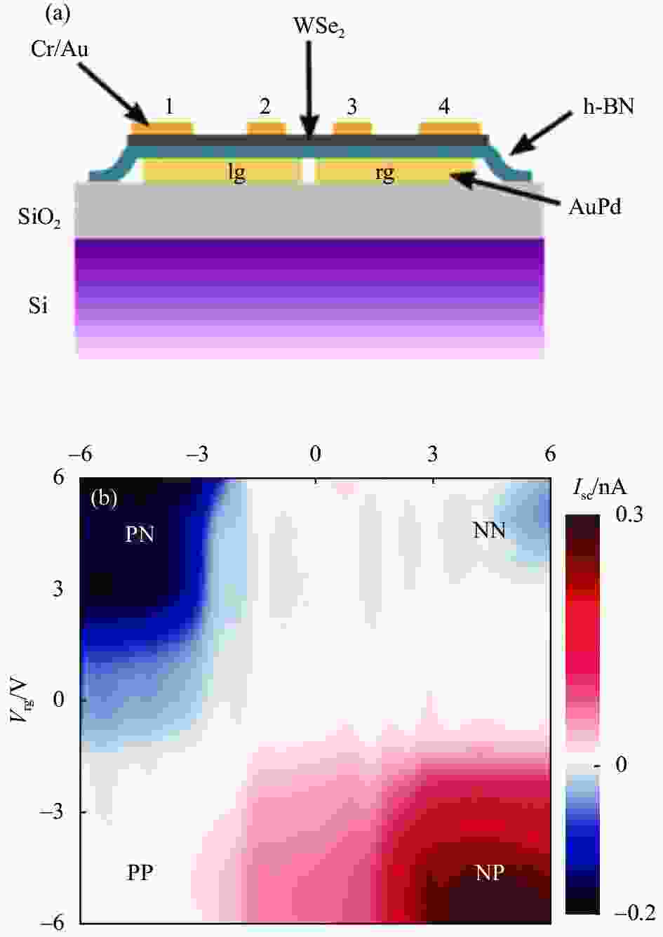
Figure 1. Split-gate tuning of WSe2 photodetector: (a) Device schematic of the double-gated WSe2 device; (b) 2D gate map of short-circuit current
局域温度场调控则基于二维材料中的光热电效应,通过光照产生非平衡热载流子,在材料中形成温度梯度分布,进而实现热电转换。这与最近备受关注的石墨烯-旋角电子学密切相关:作为一类独特的调制手段,通过以一定角度堆叠双层石墨烯,形成摩尔超晶格,将使体系的塞贝克系数发生变化,进而导致器件的光响应特性发生变化。基于此,Koppens等通过近场红外扫描光电流显微镜探测旋角石墨烯中的光电流、载流子密度空间分布,揭示了体系的光热电响应规律,展示了石墨烯摩尔超晶格在新型红外探测技术上的巨大潜力,这一结果发表在Nature Communications中[4]。
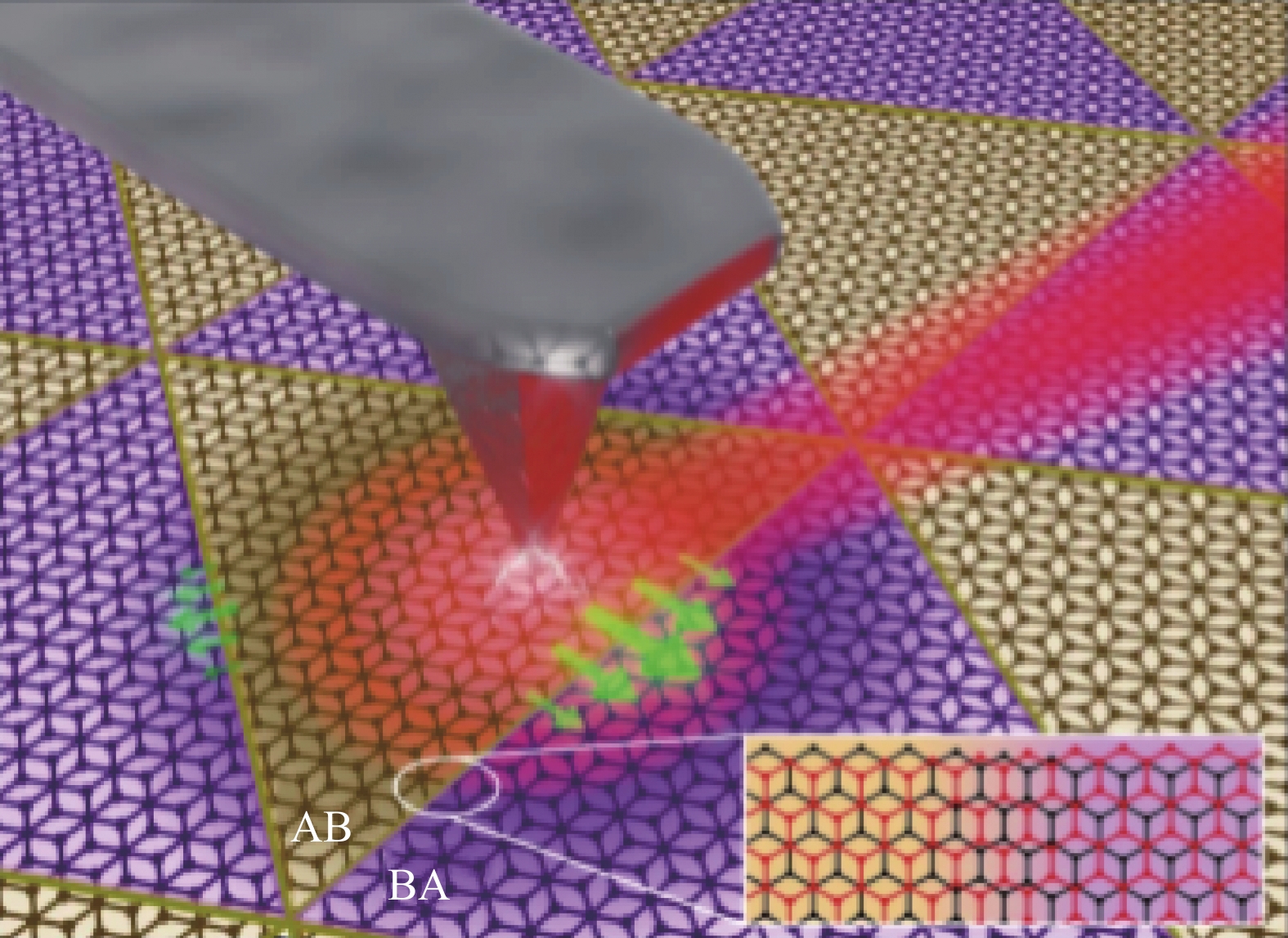
当两层石墨烯间的旋角小于0.1°时,形成的摩尔晶格周期在100 nm量级,与石墨烯中固有的红外等离子体极化波长相当,使得该体系成为一种独特的光子晶体,被称为“最小旋角双层石墨烯”(mTBG)[5]。Koppens等通过机械剥离、干法转移在Si/SiO2衬底上制备了hBN/mTBG/hBN的范德瓦尔斯异质结, 双层石墨烯间旋角为0.1°。器件的底部包含用于探测光电流信号的金电极,以及调控载流子浓度的Si背栅。实验中,施加栅压使石墨烯中的掺杂浓度达到n~5×1012 cm−2。位于器件上方的近场红外扫描光电流显微镜的探针尖端半径为20~30 nm,将能量为188 eV的红外激光聚焦于探针尖端,此时温度达到数千K,产生的热量在100 nm量级的长度范围内传播,由光热电效应产生的温度、电子密度梯度在空间上形成电荷传输。于是扫描尖端附近的区域,得到纳米级分辨率的局部光场诱导的光电流空间分布,如图2所示。
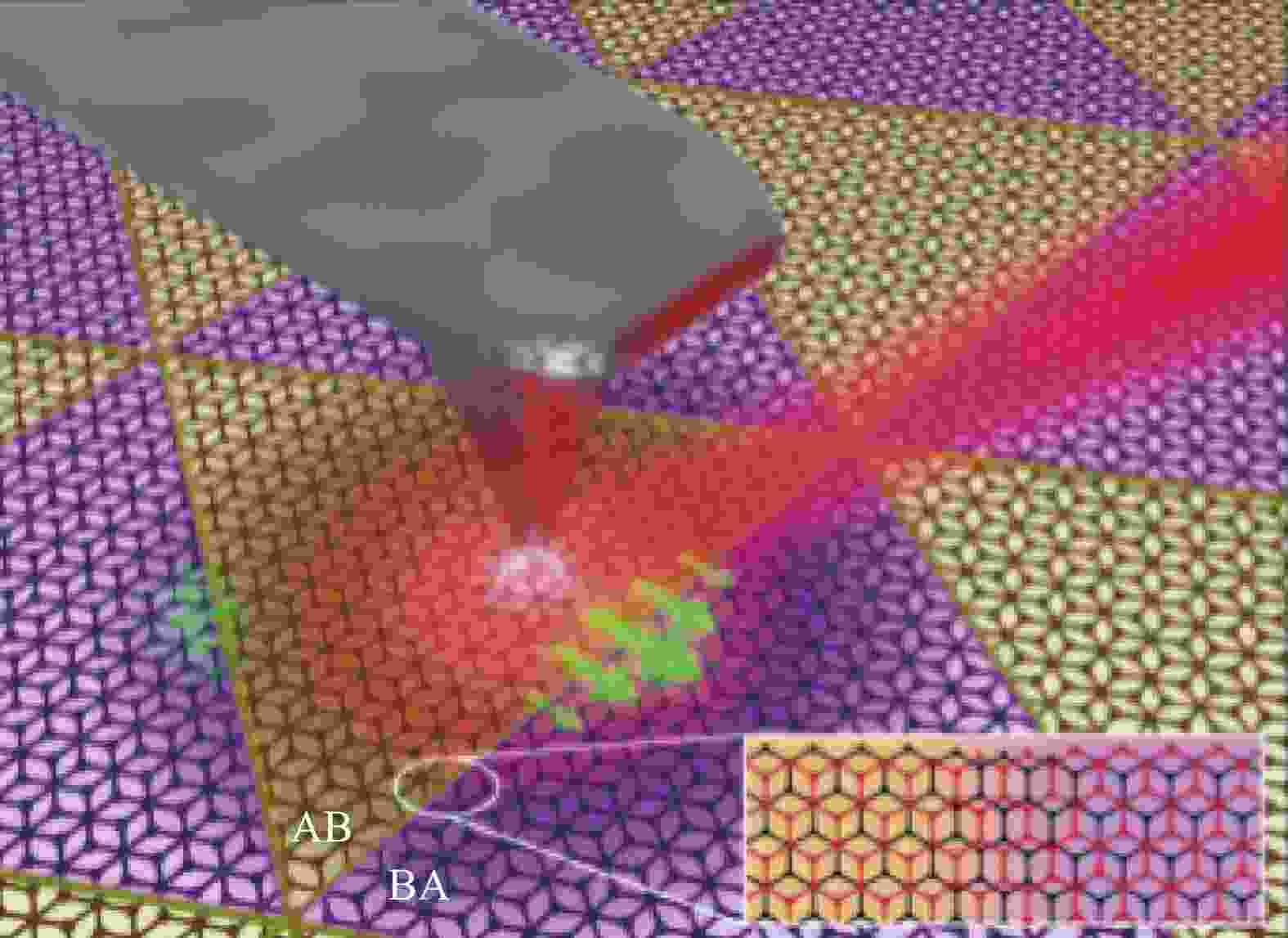
Figure 2. The AFM tip couples infrared light to the mTBG (Yellow or purple area represents the Moiré domains of different stacking configuration, respectively)
通过适当的栅极电压调制,测试结果表明器件中光电流的空间分布具有高度周期性。由于石墨烯的旋角存在一定的局部变化(0.01°~0.1°),在器件不同区域周期表现为100~1000 nm间不等。最小旋角双层石墨烯中产生由窄畴壁(6~9 nm)分隔的AB/BA伯尔纳型三角形周期结构[6],使得光电流在畴壁边界两侧发生符号反转。为了验证光热电效应带来的影响,Koppens等引入了理论模型进行对比。在该模型下,当尖端产生频率为ω的电场,器件中感应出相应的振荡电流密度,电子气中产生焦耳热,其功率密度与电流的平方成正比。热量在器件中以一定的冷却长度进行传播,并通过塞贝克-珀尔贴效应在塞贝克系数梯度下产生净电流。获得的塞贝克系数空间分布显示,塞贝克系数在畴壁附近急剧下降。通过塞贝克系数分布得到的光电流空间分布,与实验结果拟合,结果显示两者具有高度的一致性,验证了双层旋角石墨烯中光热电效应主导的光响应特性。
该工作揭示了旋角电子学在新型光电探测技术领域的前景。为了将最小旋角双层石墨烯器件的这一特性应用至光电探测中,可以将电子显微镜探针替换为纳米级金属棒,将光照下的电流信号收集并提取至外部电路。通过改变两层石墨烯间旋角的大小,可以调节摩尔晶格的周期性尺寸,使光电流符号反转的区域长度进一步缩小,使得未来的单光子探测器应用成为可能。
Near-field nano-imaging of graphene Moiré superlattices (invited)
doi: 10.3788/IRLA20211118
- Received Date: 2021-12-29
- Rev Recd Date: 2022-04-10
- Available Online: 2022-08-05
- Publish Date: 2022-08-05
Abstract: Two-dimensional materials with excellent photoresponse have presented high potential in new-type infrared photodetection technologies. Introducing a localized field into two-dimensional infrared photodetectors can greatly enhance their photodetection performance. An infrared detection technique is presented based on the photothermoelectric effect through twisted bilayer graphene Moiré superlattices. The formation of the Moire superlattice alters the Seebeck coefficient of the system and the concentration of hot carriers. Applying a high-resolution photocurrent tip is capable of detecting photoresponse of a single Moire unit cell, thereby obtaining a high-resolution photocurrent map of the whole twisted bilayer graphene system. This technique demonstrates the prospect of spintronics in the field of photodetection, and provides a novel pattern for designing future single-photon detectors.

 DownLoad: