Volume 51 Issue 7
Aug.  2022
Turn off MathJax
Article Contents

Li Shuhui, Song Hongxiao, Cheng Yazhou. Fabrication and characterization of ridge waveguide in MgF2 crystal at mid-infrared 4 μm wavelength (invited)[J]. Infrared and Laser Engineering, 2022, 51(7): 20220441. doi: 10.3788/IRLA20220441
Citation: Li Shuhui, Song Hongxiao, Cheng Yazhou. Fabrication and characterization of ridge waveguide in MgF2 crystal at mid-infrared 4 μm wavelength (invited)[J]. Infrared and Laser Engineering, 2022, 51(7): 20220441. doi: 10.3788/IRLA20220441

Fabrication and characterization of ridge waveguide in MgF2 crystal at mid-infrared 4 μm wavelength (invited)

doi: 10.3788/IRLA20220441
Funds:  National Natural Science Foundation of China (11805113);Education and Teaching Reform Research Project of Shandong University (2022 Y068);The Future Program for Young Scholars of Shandong University and Fundamental Research Funds for the Central Universities.
  • Received Date: 2022-06-25
  • Rev Recd Date: 2022-07-03
  • Available Online: 2022-08-05
  • Publish Date: 2022-08-05
  • To study the mechanism of interaction between ions and mid-infrared crystals and explore the preparation and properties of mid-infrared crystal optical waveguides, an optical ridge waveguide with a depth of 17.5 μm and a width of 14 μm was fabricated in MgF2 crystals by ion irradiation combined with precision diamond blade dicing. The SRIM software was used to simulate the process of electronic and nuclear stopping powers of MgF2 crystal irradiated by C5+ ions, and the mechanism of waveguide formation was analysed. The refractive index variation of the waveguide was simulated, and the near-field mode of the waveguide was experimentally measured and theoretically simulated. The propagation loss of the waveguide was reduced to 0.4 dB/cm by thermal annealing. The micro-Raman spectra show that there was no significant lattice damage in the waveguide region of the MgF2 crystal during ion irradiation. The results show that ion irradiation combined with diamond dicing is a very mature method to prepare ridge waveguides, and the prepared MgF2 crystal ridge waveguides have a wide application prospects in the field of mid-infrared integrated optics and optical communication.
  • [1] Zhu J Q, Zhu H, Xu H L, et al. Ge-based mid-infrared blocked-impurity-band photodetectors [J]. Infrared Physics & Technology, 2018, 92: 13-17.
    [2] Woyessa G, Kwarkye K, Dasa M K, et al. Power stable 1.5-10.5 µm cascaded mid-infrared supercontinuum laser without thulium amplifier [J]. Optics Letters, 2021, 46(5): 1129-1132. doi:  10.1364/OL.416123
    [3] Wu T, Kong W P, Wang M Y, et al. Compact hollow waveguide mid-infrared gas sensor for simultaneous measurements of ambient CO2 and water vapor [J]. Journal of Lightwave Technology, 2020, 38(16): 4580-4587. doi:  10.1109/JLT.2020.2990977
    [4] Pi M Q, Zheng C T, Zhao H, et al. Mid-infrared CHG-on-MgF2 waveguide gas sensor based on wavelength modulation spectroscopy [J]. Optics Letters, 2021, 46(21): 4797-4800.
    [5] Dodge M J. Refractive properties of magnesium fluoride [J]. Applied Optics, 1984, 23(12): 1980-1985. doi:  10.1364/AO.23.001980
    [6] Murphy E J. Integrated optical circuits and components: design and applications [M]. Boca Raton: CRC Press, 1999.
    [7] McNab S J, Moll N, Vlasov Y A. Ultra-low loss photonic integrated circuit with membrane-type photonic crystal waveguides [J]. Optics Express, 2003, 11(22): 2927-2939. doi:  10.1364/OE.11.002927
    [8] Jia Y C, Wang S X, Chen F. Femtosecond laser direct writing of flexibly configured waveguide geometries in optical crystals: fabrication and application [J]. Opto-Electronic Advances, 2020, 3(10): 190042. doi:  10.29026/oea.2020.190042
    [9] Jia Y C, Wang L, Chen F. Ion-cut lithium niobate on insulator technology: Recent advances and perspectives [J]. Applied Physics Reviews, 2021, 8: 011307. doi:  10.1063/5.0037771
    [10] Yang Q X, Liu H L, He S, et al. Circular cladding waveguides in Pr: YAG fabricated by femtosecond laser inscription: Raman, luminescence properties and guiding performance [J]. Opto-Electronic Advances, 2021, 4(2): 200005. doi:  10.29026/oea.2021.200005
    [11] Liu T, Yao Y C, Liu F R, et al. Enhanced Raman intensity in ZnS planar and channel waveguide structures via carbon ion implantation [J]. Optical Materials, 2021, 112: 110733. doi:  10.1016/j.optmat.2020.110733
    [12] Li R, Sun L F, Cai Y J, et al. Near-infrared lasing and tunable upconversion from femtosecond laser inscribed Nd, Gd: CaF2 waveguides [J]. Chinese Optics Letters, 2021, 19(8): 081301. doi:  10.3788/COL202119.081301
    [13] Li R, Nie W J, Lu Q M, et al. Femtosecond-laser-written superficial cladding waveguides in Nd: CaF2 crystal [J]. Optics & Laser Technology, 2017, 92(1): 163-167.
    [14] Zhang L M, Guo T Y, Ren Y Y, et al. Cooperative up-converted luminescence in Yb, Na: CaF2 cladding waveguides by femtosecond laser inscription [J]. Optics Communications, 2019, 441(15): 8-13.
    [15] Jia Y C, Chen F, Vazquez de Aldana J R, et al. Femtosecond laser micromachining of Nd: GdCOB ridge waveguides for second harmonic generation [J]. Optical Materials, 2012, 34(11): 1913-1916. doi:  10.1016/j.optmat.2012.05.032
    [16] Jia Y C, Dong N N, Chen F, et al. Continuous wave ridge waveguide lasers in femtosecond laser micromachined ion irradiated Nd: YAG single crystals [J]. Optical Materials Express, 2012, 2(5): 657-662. doi:  10.1364/OME.2.000657
    [17] Tan Y, Luan Q F, Liu F Q, et al. Swift carbon ion irradiated Nd: YAG ceramic optical waveguide amplifier [J]. Optics Express, 2013, 21(12): 13992-13997. doi:  10.1364/OE.21.013992
    [18] Siebenmorgen J, Petermann K, Huber G, et al. Femtosecond laser written stress-induced Nd: Y3Al5O12 (Nd: YAG) channel waveguide laser [J]. Applied Physics B, 2009, 97: 251-255. doi:  10.1007/s00340-009-3697-3
  • 加载中
通讯作者: 陈斌, bchen63@163.com
  • 1. 

    沈阳化工大学材料科学与工程学院 沈阳 110142

  1. 本站搜索
  2. 百度学术搜索
  3. 万方数据库搜索
  4. CNKI搜索

Figures(6)

Article Metrics

Article views(212) PDF downloads(40) Cited by()

Related
Proportional views

Fabrication and characterization of ridge waveguide in MgF2 crystal at mid-infrared 4 μm wavelength (invited)

doi: 10.3788/IRLA20220441
  • 1. National Demonstration Center for Experimental Physics Education, School of Physics, Shandong University, Jinan 250100, China
  • 2. Faculty of Information Science and Engineering, Ocean University of China, Qingdao 266100, China
Fund Project:  National Natural Science Foundation of China (11805113);Education and Teaching Reform Research Project of Shandong University (2022 Y068);The Future Program for Young Scholars of Shandong University and Fundamental Research Funds for the Central Universities.

Abstract: To study the mechanism of interaction between ions and mid-infrared crystals and explore the preparation and properties of mid-infrared crystal optical waveguides, an optical ridge waveguide with a depth of 17.5 μm and a width of 14 μm was fabricated in MgF2 crystals by ion irradiation combined with precision diamond blade dicing. The SRIM software was used to simulate the process of electronic and nuclear stopping powers of MgF2 crystal irradiated by C5+ ions, and the mechanism of waveguide formation was analysed. The refractive index variation of the waveguide was simulated, and the near-field mode of the waveguide was experimentally measured and theoretically simulated. The propagation loss of the waveguide was reduced to 0.4 dB/cm by thermal annealing. The micro-Raman spectra show that there was no significant lattice damage in the waveguide region of the MgF2 crystal during ion irradiation. The results show that ion irradiation combined with diamond dicing is a very mature method to prepare ridge waveguides, and the prepared MgF2 crystal ridge waveguides have a wide application prospects in the field of mid-infrared integrated optics and optical communication.

    • 红外波段根据波长的不同可以分为近红外、中红外和远红外,中红外波段最适宜进行红外光谱的测量和分析。中红外光谱技术是一种十分方便快捷且无损伤的定性定量分析方法,广泛应用于生物技术、医药卫生及各种新型材料的研发过程。中红外波段不仅可以应用于多种物质的分析与鉴定,同时在激光制导、多种复杂环境探测领域也有十分广泛的应用[1-3]。氟化镁(MgF2)晶体具有优良的光学和热机械性能,优异的偏振性,可以用于制作偏光元件。MgF2晶体透射窗口覆盖了大多数气体的中红外吸收带,是现有红外材料中自身透过率最高的,在2 mm厚度时对中红外波段的光束透过率可达 90%以上,且具有较高的耐用性,是制造棱镜和透镜的理想窗口材料,广泛应用于红外激光制导及光电雷达等红外跟踪、探测系统中[4-5]。集成光学是运用光学理论知识,将各种微型光学元件微型化集成在同一衬底上来实现复杂功能的新型学科。集成光学器件具有体积小、功能齐全、性能稳定、易于与其他设备相结合的优点,且效率高、功耗低、使用方便、成本低[6-7]。光波导是集成光学中的基本元件,波导传输性能会直接影响集成光学系统的性能。光波导作为集成光学的基本元件,是由折射率较低的区域包裹折射率较高的区域构成的,利用光在折射率不同的两种物质界面上的全反射原理,将光波限制在微米量级的微小结构内传输并且达到较高的光密度[8]。当前,常见的光波导的制备方法有飞秒激光直写、载能离子束辐照、分子束外延与脉冲激光沉积等[9-15]。载能离子辐照技术是利用高速离子辐照衬底材料,高速离子与衬底材料中的电子与原子核发生碰撞,造成电子损伤和核能量损伤,从而改变衬底材料表面的折射率使其满足全光学全反射原理形成光波导结构[16-17]。相比于其他波导制造方法,载能离子辐照技术不受温度限制,已成功在多种材料制备出光波导结构。笔者采用了离子辐照表面改性技术制备平面波导结构,然后采用金刚石刀切割的精密加工技术在平面波导结构上切割出脊形光波导,研究MgF2晶体脊形光波导在中红外4 µm波长下的折射率分布、近场模式及传输损耗等特性,并利用拉曼光谱来研究离子辐照对MgF2晶体的晶格损伤情况。

    • 首先,准备了一块z切向的六个表面都进行抛光处理的(10 mm×10 mm×2 mm) MgF2晶体。然后,利用串列加速器(中国科学院半导体研究所),采用快重离子辐照技术将能量为25 MeV、剂量为2×10¹¹ ion/cm2 的C5+离子辐照到晶体表面(10 mm×2 mm),离子束密度控制在10~30 nA/cm2来避免热效应和电荷效应,同时将入射离子束角度设定为7°来降低沟道效应,如图1(a)所示。随后,使用精密金刚石刀划片机AR3000(江苏京创先进电子科技有限公司)对制备的样品进行微加工。将划片机的主轴旋转速度设定为30000 rpm,刀片行进速度为0.1 mm/s,在MgF2晶体表面切割出相距14 μm的两条平行沟槽。脊形光波导的宽度由两沟槽间距确定,如图1(b)所示。经过上述操作流程,在MgF2晶体表面制备出了深度为17.5 μm、宽度为14 μm的脊形光波导。

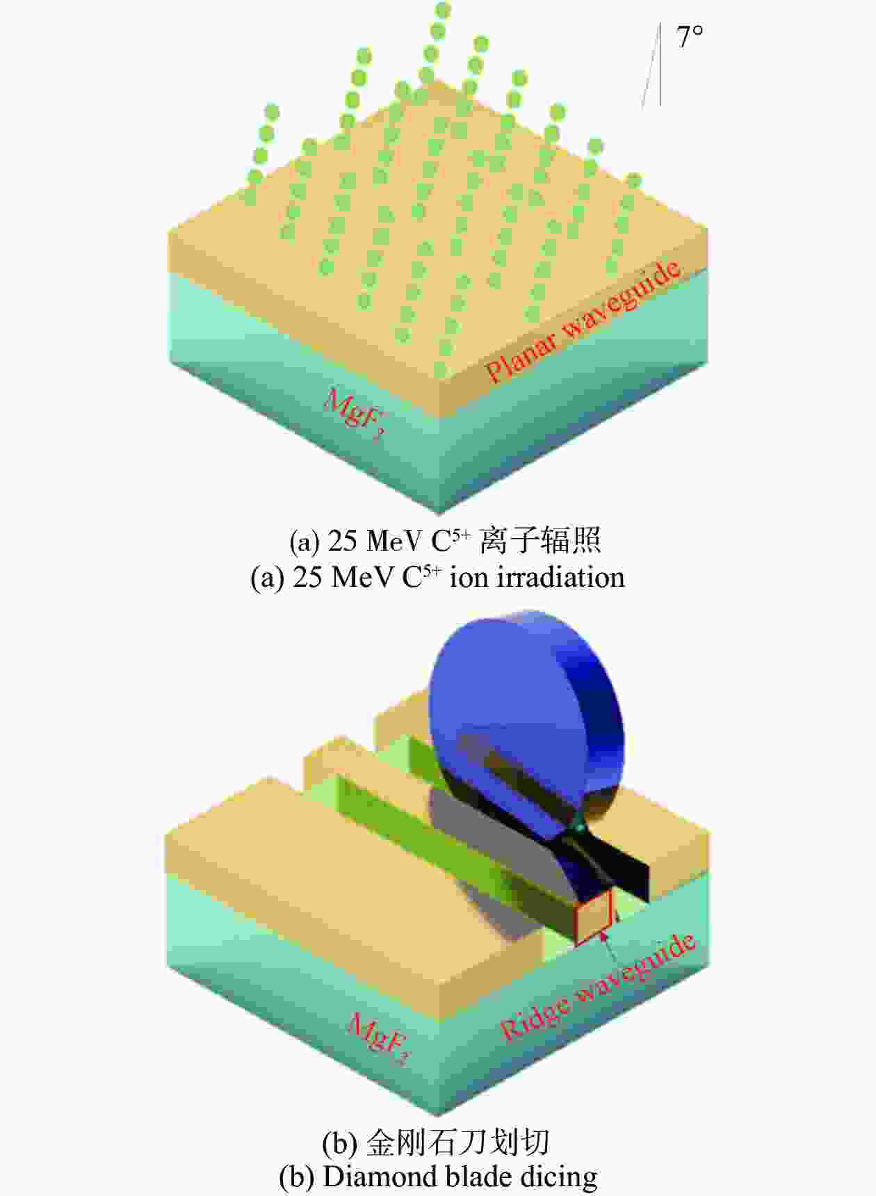
      Figure 1.  Schematic diagram of preparation process of MgF2 ridge optical waveguide

    • 为了研究制备出的MgF2晶体脊形光波导的传输特性,搭建了端面耦合系统,如图2所示。激光光源为可调谐激光系统MIRTM 8025,产生波长为4 μm的中红外光束,经偏振器后,由一个中红外物镜Obj1 (ZnSe, LFO-5-12-3.75, N.A.=0.13)对光束进行聚焦,然后耦合进入脊形光波导,光束经过脊形光波导后出射,并被另一个中红外物镜Obj2 (ZnSe, LFO-5-12-3.75, N.A.= 0.13)聚焦。最后,使用中红外探测器(Tigris-640, Xenics)来记录光的近场模式,同时利用中红外光功率计(PM125 D, Thorlabs)测量入射光束和出射光束的光功率,计算出波导的传输损耗。在偏振器和物镜Obj1之间放置一个ZnSe玻璃立方体,通过旋转玻璃立方体,测量了当透射光消失所对应的光波导的最大受光角,从而计算晶体光波导的最大折射率变化值。

      Figure 2.  Schematic diagram of end-face coupling system for optical waveguide

      为进一步优化波导的传输性能,利用热退火技术对波导进行处理。将波导样品依次进行五次退火处理,退火温度依次设定为180 ℃、220 ℃、260 ℃、300 ℃和340 ℃,每次退火时间设置为1 h。在每次退火处理后计算波导的传输损耗。最后利用共焦拉曼光谱仪对波导样品的波导层(脊形波导的表面位置)和衬底层进行拉曼光谱的测量,研究离子辐照技术对MgF2晶格结构的影响。

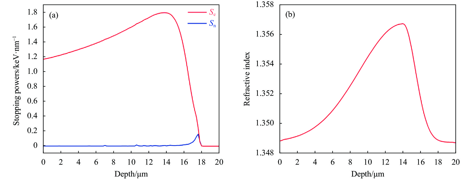
    • 利用SRIM软件模拟了离子辐照过程中原子核和电子能量的沉积过程,绘制了电子能量损伤Se和原子核能量损伤Sn随辐照深度变化关系,如图3(a)所示。可以看出,在0~17.6 µm深度范围内,Se显著高于Sn,在14 µm深度处,Se达到峰值1.8 keV/nm,然后逐渐降低,直至0。在0~16 μm深度范围内,Sn值为0,然后逐渐增大,在17.5 μm深度处达到最大值0.156 keV/nm,然后逐渐降低,在18 μm深度处Sn值降为0。通过比较SnSe的数值大小可以看到,电子能量损伤在引起波导折射率变化过程中占据主导地位。

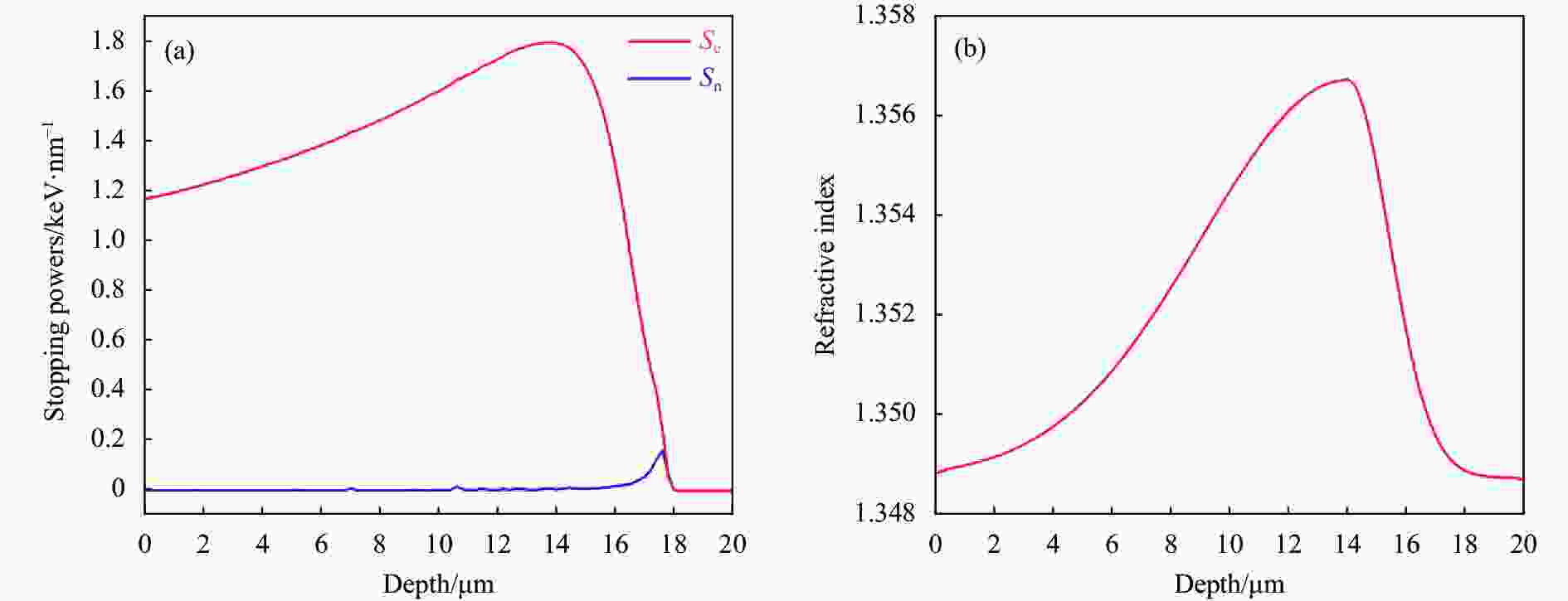
      Figure 3.  (a) Relation of electronic energy damage (red line) and nuclear energy damage (blue line) with the irradiation depth of C5+ ions; (b) Reconstructed relation of refraction index of MgF2 ridge waveguide with the waveguide depth at 4 μm wavelength

    • 由于制备的光波导结构无法采用暗模光谱法测量中红外波长下的折射率分布。为了计算波导中最大折射率变化值Δn,使用公式[18]

      式中:n = 1.3488为MgF2材料在波长为4 μm时的折射率;Θm为波导的最大受光角。通过端面耦合系统测量得到Θm = 8.4°,计算出了最大折射率变化Δn= 0.008。根据电子能量损伤随波导深度的变化,结合计算出的波导最大折射率变化,重建了波导折射率与波导深度之间的关系,如图3(b)所示[16]

    • 利用显微镜拍摄制备出的脊形光波导的端面图像来确定波导的具体尺寸,波导宽度为14 μm,深度为17.5 μm,如图4(a)所示。通过端面耦合实验,发现MgF2晶体脊形光波导的近场模式呈现单模传输,如图4(b)所示。根据重建的折射率与波导深度之间的关系,使用Rsoft软件基于有限差分光束传播法(FD-BPM)模拟4 μm波长下MgF2脊形光波导近场模式,如图4(c)所示。通过比较图4(b)和图4(c)可以看出,二者图像吻合较好,证明重建的波导折射率分布和Rsoft软件模拟的结果是正确的。

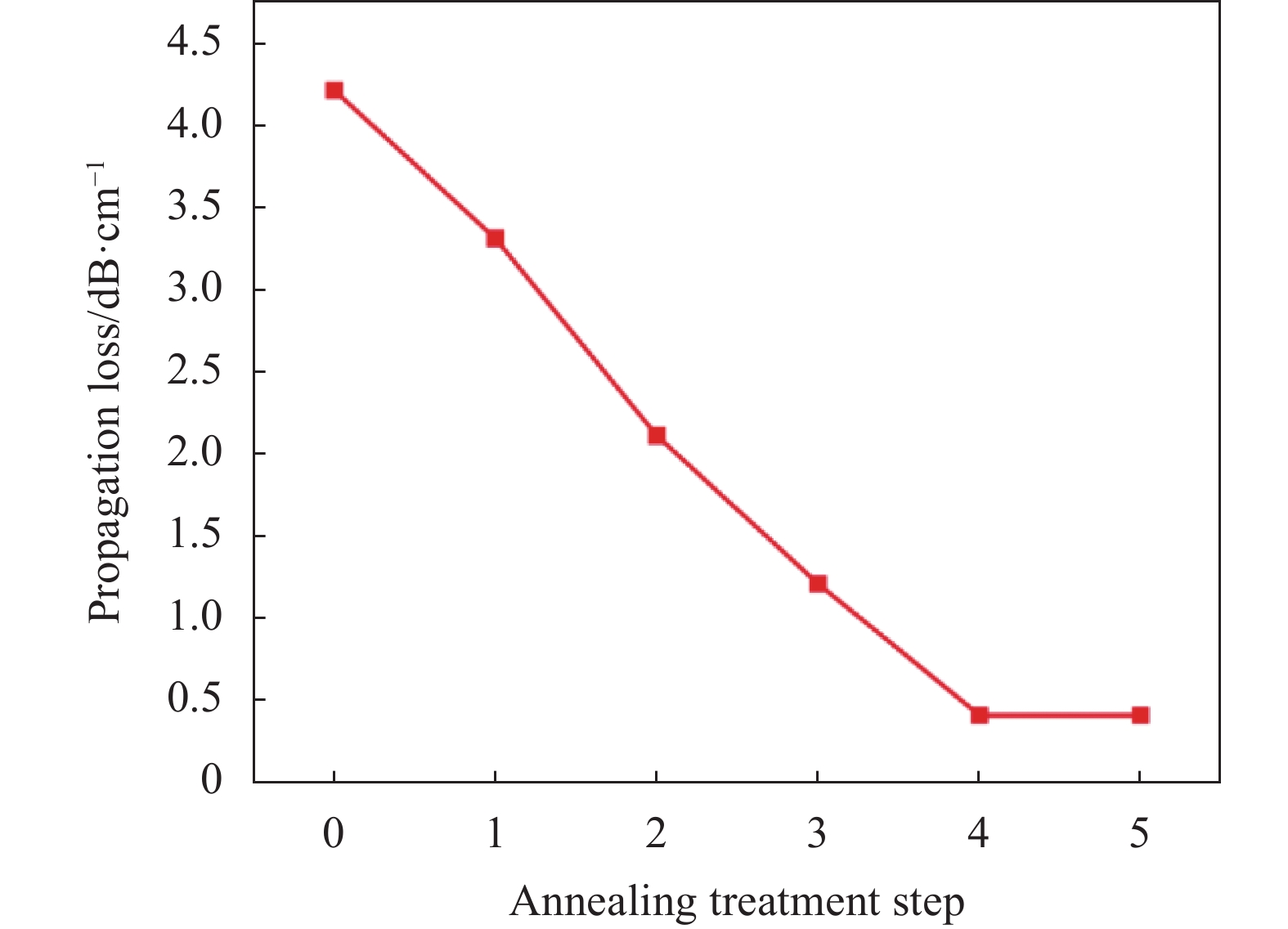
    • 热退火处理可以消除离子辐照过程中产生的色心和点缺陷,从而进一步降低波导的传输损耗。基于端面耦合系统测量的波导入射功率和出射功率,计算每次退火处理后脊形光波导在4 μm波长下的传输损耗,如图5所示。可以看出,退火处理前波导的传输损耗为4.2 dB/cm,经过五次退火处理后,传输损耗依次降低到3.3 dB/cm、2.1 dB/cm、1.2 dB/cm、0.4 dB/cm和0.4 dB/cm。经第五次退火处理后,脊形光波导的传输损耗不变,表明脊形光波导在300~340 ℃具有良好的热稳定性。实验证明,热退火处理可以有效地优化波导的传输性能,降低传输损耗。

      Figure 4.  Sectional microscopic image of optical ridge waveguide; (b) Experimental diagram of near-field mode distribution at 4 μm wavelength; (c) Simulated diagram of near-field mode distribution at 4 μm wavelength of optical ridge waveguide

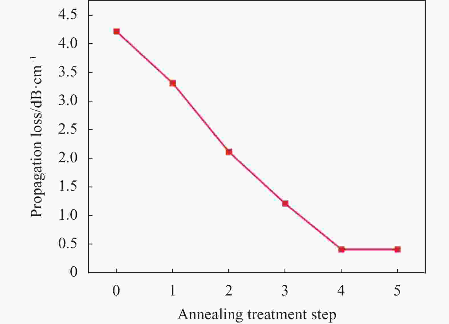
      Figure 5.  Relation diagram of propagation loss of MgF2 optical ridge waveguide after thermal annealing treatment

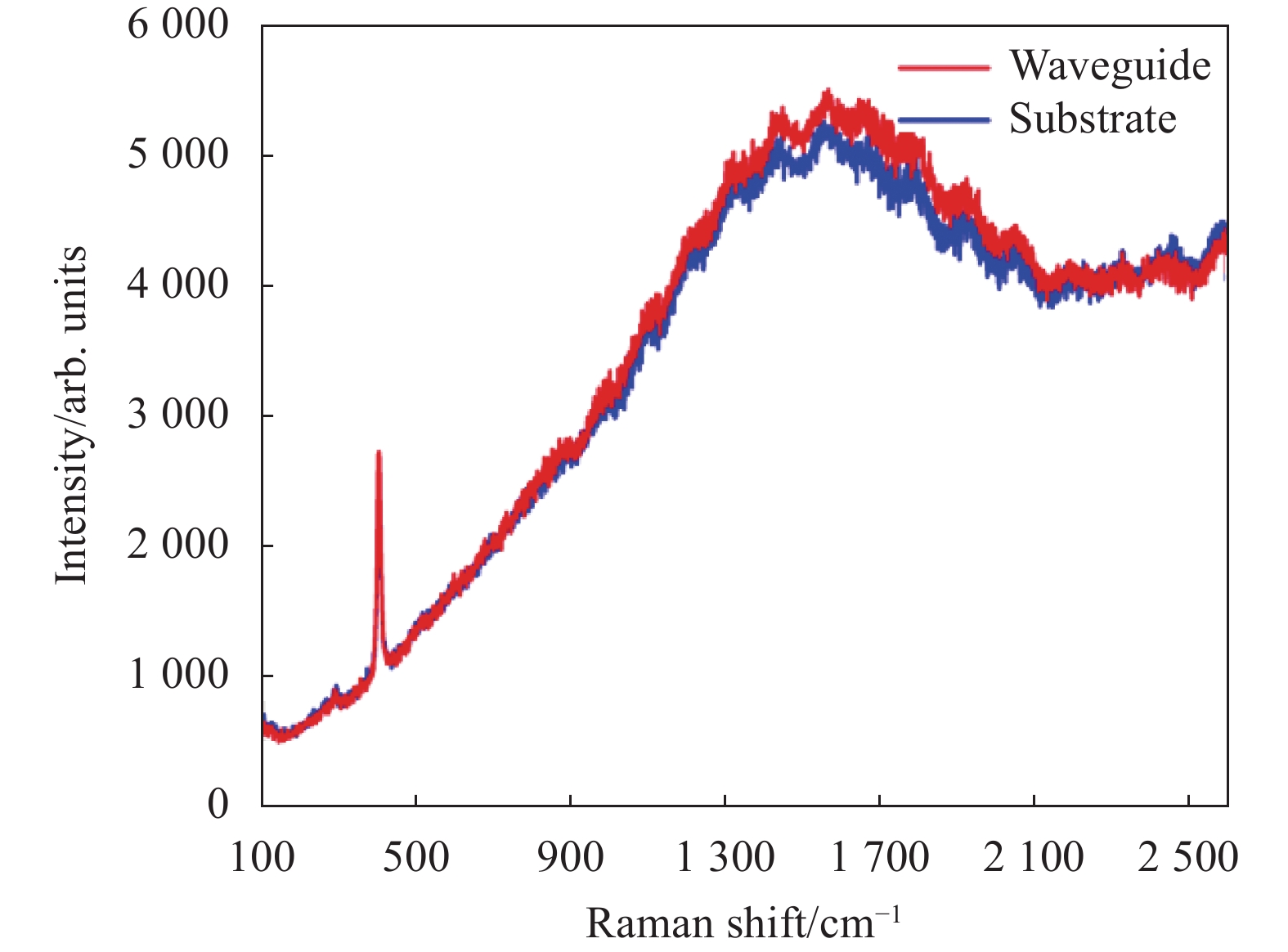
    • 图6为离子辐照制备的MgF2晶体波导层和衬底层的拉曼光谱。可以看出,波导层和衬底层的拉曼光谱的峰强、峰宽和峰位基本一致,证明C5+离子辐照对MgF2晶体并未造成较大的晶格损伤。

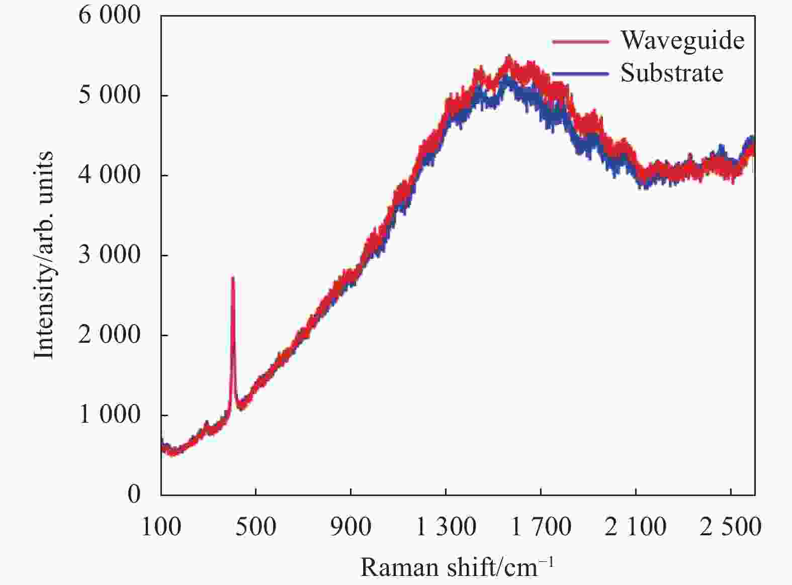
      Figure 6.  Raman spectra of waveguide layer and substrate layer of MgF2 crystal material

    • 使用能量为25 MeV、剂量为2 × 10¹¹ ion/cm2的C5+离子辐照MgF2晶体表面制备出平面光波导结构,然后使用精密金刚石切割技术制备出MgF2脊形光波导。通过端面耦合系统测试发现,在中红外4 μm波长下,波导的近场光强分布呈现单模传输。采用热退火技术对制备的MgF2脊形光波导进行性能优化,最终将脊形光波导的传输损耗降至0.4 dB/cm。拉曼光谱证明离子辐照技术并未对MgF2材料造成较大的晶格损伤。该工作表明,离子辐照技术结合划片机精密切割是一种十分成熟的脊形波导制备手段,制备的MgF2晶体脊形光波导在中红外集成光学和光通讯领域具有广泛的应用前景。

Reference (18)

Catalog

    /

    DownLoad:  Full-Size Img  PowerPoint
    Return
    Return