Volume 52 Issue 9
Sep.  2023
Turn off MathJax
Article Contents

Shao Jiaqi, Chen Honglei, Ding Ruijun. Linear APD hybrid time-of-flight ranging model and readout circuit design[J]. Infrared and Laser Engineering, 2023, 52(9): 20220892. doi: 10.3788/IRLA20220892
Citation: Shao Jiaqi, Chen Honglei, Ding Ruijun. Linear APD hybrid time-of-flight ranging model and readout circuit design[J]. Infrared and Laser Engineering, 2023, 52(9): 20220892. doi: 10.3788/IRLA20220892

Linear APD hybrid time-of-flight ranging model and readout circuit design

doi: 10.3788/IRLA20220892
  • Received Date: 2022-10-20
  • Rev Recd Date: 2022-12-25
  • Publish Date: 2023-09-28
  •   Objective  Currently, 3D image sensors based on time-of-flight ranging have been widely used in military and civil applications, such as astronomical detection, target identification, and unmanned vehicles. They are currently being developed in the direction of high sensitivity, high accuracy, and low power consumption in the future. Hybrid time-of-flight ranging, which can achieve high accuracy and high range of lidar ranging, is based on the principle of indirect time-of-flight ranging while incorporating the notion of direct time-of-flight ranging. It has become one of the development paths of time-of-flight ranging. For this purpose, a hybrid ranging model and a 5×5 array readout circuit with 50 µm center distance are designed based on an APD in linear mode as the detector.  Methods  A two-segment, two-phase hybrid ranging model is built in this paper (Fig.4). Based on this model, the time-of-flight solution was implemented and the error of background light and counter clock frequency was simulated (Fig.6-7). In order to adapt to the model, the readout circuit selects Capacitor Feedback Transimpedance Amplifier (CTIA) as the input stage, outputs a voltage signal through a sample-and-hold circuit, and generates an 8-bit digital signal through a positive feedback comparator and True Single Phase Clock counter (Fig.3). The accuracy of intensity information is determined by calculating the linearity of the analog voltage output (Fig.9). The accuracy of distance measurement is analyzed by combining analog and digital signals, calculating the time of flight in the vicinity of 108.75 m, and comparing the result to the ideal value (Fig.10).  Results and Discussions  The hybrid ranging readout circuit can be passively integrated over a range of 0.5 V to 2.5 V with high injection efficiency. CTIA output voltage has 99.83% linearity (Fig.9). In the hybrid ranging simulations over a range of 108.75 m, the K values were correctly determined for most subperiods. The maximum and average errors in the last subperiod are 11.355 cm and 4.415 cm respectively (Fig.10). This error can be greatly reduced by optimizing the data at the first and last ends. Performance of the readout circuit meets design requirements. The simulation results of the main parameters are compared with the advanced designs at home and abroad in various ranging modes (Tab.1). It can be seen that the small array readout circuit based on LM-APD in the paper achieves a much higher range than indirect ranging at a lower modulation frequency using a medium process. It also achieves a higher accuracy with a very low counter cost and good linearity compared with the direct ranging scheme. It provides a hybrid ranging scheme that can be applied to near-medium range.  Conclusions  In this study, a hybrid ranging model is established and systematically analyzed by combining the advantages of direct ranging and indirect ranging. Based on the model, the intensity of reflected background light and continuous pulse light can be found. By using LM-APD, a 5×5 array with 50-μm pixel center distance two-stage two-phase hybrid ranging readout circuit is designed. It consists of two sub-frames of phase in a single frame, with two steps of integration process in each sub-frame. Both a voltage analog output and an 8 bit counter digital output are available from the readout circuit, which employs CTIA as its input stage. Simulation results show that the analog output achieves 99.83% linearity at a modulation frequency of 20 MHz, and the readout circuit achieves a maximum error of 11.355 cm and an average error of 4.415 cm over a hybrid ranging range of 108.75 m. It extends the range to 29 times that of pure indirect ranging, and the readout circuit has great potential for key performance such as accuracy and range. The preliminary simulation results have shown the advantages of hybrid ranging and verified the feasibility of the hybrid ranging model, providing a theoretical and circuit reference for the design of a larger-scale infrared focal plane 3D imaging readout circuit. Further validation and improvement are pending after the flow of the chip.
  • [1] Cao Jie, Hao Qun, Zhang Fanghua, et al. Research progress of APD three-dimensional imaging lidar [J]. Infrared and Laser Engineering, 2020, 49(9): 20190549. (in Chinese) doi:  10.3788/IRLA20190549
    [2] Hao Q, Tao Y, Cao J, et al. Development of pulsed-laser three-dimensional imaging flash lidar using APD arrays [J]. Microw Opt Technol Lett, 2021, 63: 2492-2509.
    [3] Hang Qiwen, Liang Qinghua, Ding Ruijun, et al. Research on testing of active and passive HgCdTe APD detector in linear mode [J]. Infrared and Laser Engineering, 2021, 50(6): 20200460. (in Chinese) doi:  10.3788/IRLA20200460
    [4] Borniol E D D, Rothman J, Guellec F, et al. Active three dimensional and thermal imaging with a 30-μm pitch 320×256 HgCdTe avalanche photodiode focal plane array [J]. Opt Eng, 2012, 51(6): 1305.
    [5] Li Xiao, Shi Zhu, Dai Qian, et al. 64×64 InGaAs/InP 3D imaging laser focal plane detector [J]. Infrared and Laser Engineering, 2018, 47(8): 0806004. (in Chinese) doi:  10.3788/IRLA201847.0806004
    [6] Wu J, Qian Z, Zhao Y. et al. 64×64 GM-APD array-based readout integrated circuit for 3D imaging applications [J]. Sci China Inf Sci, 2019, 62: 62407.
    [7] Bamji C, Godbaz J, Oh M, et al. A review of indirect time-of-flight technologies [J]. IEEE Transactions on Electron Devices, 2022, 69(6): 2779-2793.
    [8] Shcherbakova, Pancheri L, Massari N, et al. Linear-mode gain-modulated avalanche photodiode image sensor for time-of-flight optical ranging [J]. IEEE Transactions on Electron Devices, 2016, 63(1): 145-152.
    [9] Hsu T H, Liao T, Lee N A, et al. A CMOS time-of-flight depth image sensor with in-pixel background light cancellation and phase shifting readout technique [J]. IEEE Journal of Solid-State Circuits, 2018, 53(10): 2898-2905.
    [10] Okino T, Yamada S, Sakata Y, et al. 5.2 A 1 200×900 6 m 450 fps geiger-mode vertical avalanche photodiodes CMOS image sensor for a 250 m time-of-flight ranging system using direct-indirect-mixed frame synthesis with configurable depth resolution down to 10 cm[C]//2020 IEEE International Solid- State Circuits Conference - (ISSCC), 2020: 96-98.
    [11] Kawahito S, Yasutomi K, Mars K. Hybrid time-of-flight image sensors for middle-range outdoor applications [J]. IEEE Open Journal of the Solid-State Circuits Society, 2022(2): 38-49.
    [12] Payne A, Daniel A, Mehta A, et al. 7.6 A 512×424 CMOS 3D time-of-flight image sensor with multi-frequency photo-demodulation up to 130 MHz and 2 GS/s ADC[C]//2014 IEEE International Solid-State Circuits Conference(ISSCC), 2014: 134-135.
    [13] Park B, Park I, Choi W, et al. A 64×64 APD-based ToF image sensor with background light suppression up to 200 klx using in-pixel auto-zeroing and chopping [C]//2019 Symposium on VLSI Circuits, 2019: C256-C257.
    [14] Song P, Ye Z, Hu W, et al. Injection efficiency of DI and CTIA readout integrated circuit[C]//2015 International Conference on Numerical Simulation of Optoelectronic Devices (NUSOD), 2015: 81-82.
    [15] 褚培松. 高灵敏度红外焦平面大动态范围读出电路研究[D]. 上海: 中国科学院大学(中国科学院上海技术物理研究所), 2020.

    Chu Peisong. Research on high dynamic range readout integratedcircuit for high sensitivity infrared focal plane array [D]. Shanghai: University of Chinese Academy of Sciences (Shanghai Institute of Technical Physics, Chinese Academy of Sciences), 2020. (in Chinese)
  • 加载中
通讯作者: 陈斌, bchen63@163.com
  • 1. 

    沈阳化工大学材料科学与工程学院 沈阳 110142

  1. 本站搜索
  2. 百度学术搜索
  3. 万方数据库搜索
  4. CNKI搜索

Figures(10)  / Tables(1)

Article Metrics

Article views(139) PDF downloads(60) Cited by()

Related
Proportional views

Linear APD hybrid time-of-flight ranging model and readout circuit design

doi: 10.3788/IRLA20220892
  • 1. Key Laboratory of Infrared Imaging Materials and Detectors, Shanghai Institute of Technical Physics, Chinese Academy of Sciences, Shanghai 200083, China
  • 2. School of Information Science and Technology, Shanghaitech University, Shanghai 200120, China
  • 3. University of Chinese Academy of Sciences, Beijing 100049, China

Abstract:   Objective  Currently, 3D image sensors based on time-of-flight ranging have been widely used in military and civil applications, such as astronomical detection, target identification, and unmanned vehicles. They are currently being developed in the direction of high sensitivity, high accuracy, and low power consumption in the future. Hybrid time-of-flight ranging, which can achieve high accuracy and high range of lidar ranging, is based on the principle of indirect time-of-flight ranging while incorporating the notion of direct time-of-flight ranging. It has become one of the development paths of time-of-flight ranging. For this purpose, a hybrid ranging model and a 5×5 array readout circuit with 50 µm center distance are designed based on an APD in linear mode as the detector.  Methods  A two-segment, two-phase hybrid ranging model is built in this paper (Fig.4). Based on this model, the time-of-flight solution was implemented and the error of background light and counter clock frequency was simulated (Fig.6-7). In order to adapt to the model, the readout circuit selects Capacitor Feedback Transimpedance Amplifier (CTIA) as the input stage, outputs a voltage signal through a sample-and-hold circuit, and generates an 8-bit digital signal through a positive feedback comparator and True Single Phase Clock counter (Fig.3). The accuracy of intensity information is determined by calculating the linearity of the analog voltage output (Fig.9). The accuracy of distance measurement is analyzed by combining analog and digital signals, calculating the time of flight in the vicinity of 108.75 m, and comparing the result to the ideal value (Fig.10).  Results and Discussions  The hybrid ranging readout circuit can be passively integrated over a range of 0.5 V to 2.5 V with high injection efficiency. CTIA output voltage has 99.83% linearity (Fig.9). In the hybrid ranging simulations over a range of 108.75 m, the K values were correctly determined for most subperiods. The maximum and average errors in the last subperiod are 11.355 cm and 4.415 cm respectively (Fig.10). This error can be greatly reduced by optimizing the data at the first and last ends. Performance of the readout circuit meets design requirements. The simulation results of the main parameters are compared with the advanced designs at home and abroad in various ranging modes (Tab.1). It can be seen that the small array readout circuit based on LM-APD in the paper achieves a much higher range than indirect ranging at a lower modulation frequency using a medium process. It also achieves a higher accuracy with a very low counter cost and good linearity compared with the direct ranging scheme. It provides a hybrid ranging scheme that can be applied to near-medium range.  Conclusions  In this study, a hybrid ranging model is established and systematically analyzed by combining the advantages of direct ranging and indirect ranging. Based on the model, the intensity of reflected background light and continuous pulse light can be found. By using LM-APD, a 5×5 array with 50-μm pixel center distance two-stage two-phase hybrid ranging readout circuit is designed. It consists of two sub-frames of phase in a single frame, with two steps of integration process in each sub-frame. Both a voltage analog output and an 8 bit counter digital output are available from the readout circuit, which employs CTIA as its input stage. Simulation results show that the analog output achieves 99.83% linearity at a modulation frequency of 20 MHz, and the readout circuit achieves a maximum error of 11.355 cm and an average error of 4.415 cm over a hybrid ranging range of 108.75 m. It extends the range to 29 times that of pure indirect ranging, and the readout circuit has great potential for key performance such as accuracy and range. The preliminary simulation results have shown the advantages of hybrid ranging and verified the feasibility of the hybrid ranging model, providing a theoretical and circuit reference for the design of a larger-scale infrared focal plane 3D imaging readout circuit. Further validation and improvement are pending after the flow of the chip.

    • 雪崩光电二极管(Linear-Mode APD, LM-APD)具有高灵敏度、高信噪比等优势[1-2],近20年来,基于APD阵列的脉冲激光三维成像雷达因其在军事和民用方面的巨大潜力引起了广泛的研究兴趣。APD可以工作在线性模式和盖革模式。工作在线性模式下的APD(LM-APD)的输出电流与偏置电压呈线性关系,与盖革模式相比具有无死区时间、可获得强度信息等优势,能够实现连续探测目标物体的强度和时间信息[3]。LM-APD激光测距主要基于飞行时间测距的原理,飞行时间测距分为直接飞行时间测距(dToF)和间接飞行时间测距(iToF),直接飞行时间测距测量激光发射与回波的时间差,法国CEA/LETI设计的30 μm间距的320×256阵列,通过读出电路的模拟输出存储飞行时间和脉冲强度,在30 m的范围内达到了11 cm的距离分辨率[4]。西南技术物理研究所设计的64×64 铟镓砷三维成像激光焦平面利用14位时间数字转换器(TDC),通过四相时钟技术达到了1 ns的分辨率以及440 nW的功耗[5]。东南大学研发出在盖革模式下工作的64×64 APD阵列,读出电路采用两段TDC结构实现了4 090 ns的测距范围,分辨率在1 ns以下[6]。直接测距可以达到很高的测量范围,精度的提高有赖于高精度的TDC和数模转换器(ADC),会极大地提高面积和功耗。

      iToF积存反射光、检测与发射光源的相位差,其原理决定了工艺要求与被动的2D传感器高度相似[7]。特伦托大学[8]基于LM-APD,采用CTIA作为读出电路输入级,在不同的调制频率下演示了它在飞行时间相机中的操作。台湾清华大学[9]使用p+/n阱二极管翻转实现像素内背景光抵消高达180 klx,深度传感能力范围为0.75~7.5 m,线性误差低于1.1%[10]。日本静冈大学团队[11]设计的图像传感器将间接测距一般采用的50%占空比的连续脉冲波替换为极小占空比的脉冲应用于10~100 m的户外环境,这对探测器和发射器都产生了更高的要求,目前的稳定性和普适性还有待提高。

      针对直接测距与间接测距的优势和特点,文中采用两段两相测距,将直接测距与间接测距结合,提出并详细分析了混合飞行时间测距模型,基于该模型设计了适用于三维成像领域的5×5阵列读出电路结构。

    • 通过间接测距获得目标的距离信息需要组合多个不同相位的积分信息,在实际系统中,使用连续方波或正弦波调制,选取0、90、180、270相位,传统的四相测距方法如图1所示,考虑背景光以及暗电流的情况,由于反射脉冲波的强度未知,为了实现0~2$ \pi $相移测量,需要至少采集四相的信息,通过将两个相位的积分结果相减消除背景光以及暗电流的影响,通过相除来消除连续脉冲激光的平均增益。积分结果的精度主要由积分电荷量和解调对比度决定[8],深度信息可以由以下公式推得:

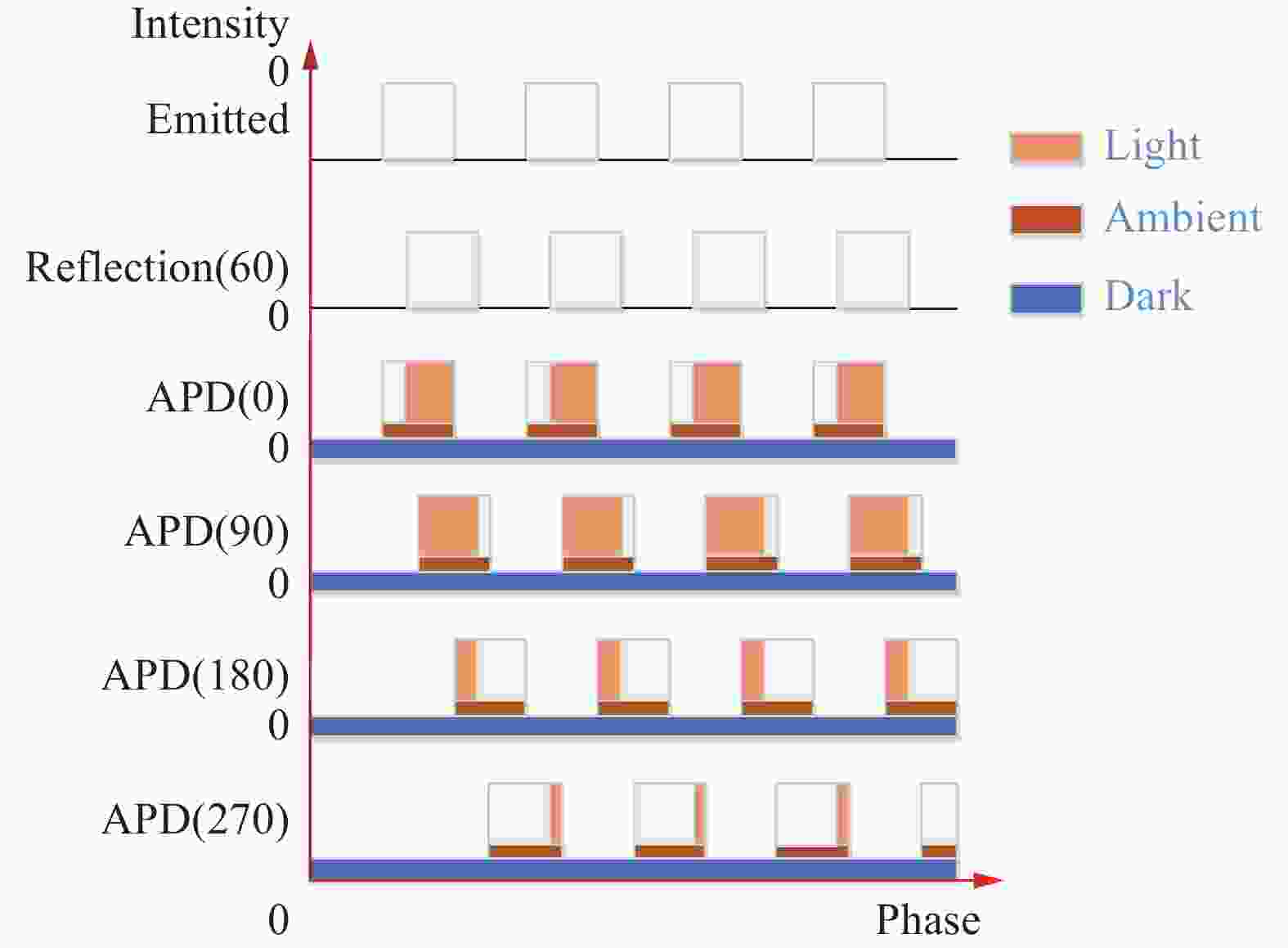
      Figure 1.  Four-phase ranging integration situation

      式中:$ c $为光速;$ {f}_{m} $为调制频率。根据公式(3)可知,间接测距可以在高调制频率下保持较高的精度,然而随着调制频率的提高,周期会越来越短,可测距离逐渐降低。当测量距离超过光在单周期内的位移,测量结果为$ \theta +2 k\pi $,这时需要进一步的手段来获取子周期数目($ k $值)才能计算实际距离,目前多频调制是求解$k $值的普遍方法,一个适用于微软xbox one的图像传感器[12]实现了高像素分辨率和低运动模糊,通过多频调制,在0.8~4.2 m的范围内实现了<1%的误差。多频调制采用两个甚至更多激光频率进行上述的相位积分,通过低频的激光提高测距范围,通过高频的激光提高测距精度,合理地调整两种频率下的积分时间,也可以进一步提高信噪比。这种测距方法存在对激光的要求高、帧率降低、功耗过大等缺点。

      文中设计在间接测距的基础上结合了直接测距的概念,同时设计了混合测距读出电路。

    • 读出电路对APD阵列输出的光电流进行积分并实现混合测距,应至少满足如下条件:1)为探测器提供稳定的偏置电压;2)较高的注入效率以及足够的带宽;3)提高间接测距的精度需要较大的电荷容量和输出摆幅;4)消除背景光和暗电流对积分的影响;5)产生满足精度的数字输出,结合数字和模拟输出实现高范围、高精度的混合测距。综合考虑面积、精度、测距范围、速度、功耗等因素,设计了一款5×5面阵、50 μm中心距像元的数模混合读出电路。

      图2为读出电路的整体结构,包括像素阵列、列共用缓冲电路、偏置电路、输出缓冲电路、反相器缓冲电路、LVDS驱动电路以及数字行列选电路等结构。

      Figure 2.  Circuit system structure

      像元是读出电路的核心,按照要求的工作时序产生数模输出,其性能直接影响精度、范围等关键指标。输出电压经过单位增益运算放大器构成的列缓冲、输出缓冲级以5 MHz的读出速率输出。计数器输出通过两组8级反相器缓冲器增大驱动能力并产生一对差分信号输出,随后通过LVDS驱动电路将CMOS信号转化为LVDS信号输出,输出速率可调。通过两组行选列选电路控制计数器数字输出和输出电压模拟输出,两种输出同时开始串行传输,读出电路的帧率取决于输出速率较低的输出(一般为模拟输出)。

    • 图3给出了单元像素电路,由CTIA输入级、斩波电路[13]、比较器、计数器、采样保持电路和缓冲电路组成。

      Figure 3.  Pixel circuit

      CTIA具有注入效率高、噪声低、线性度高的特点,可适用于不同的波长,其注入效率[14]如公式(4)所示:

      式中:${R}_{d}、{C}_{d}$为探测器的电阻和电容;${C}_{{{int}}}$为积分电容。

      为了提高增益和输出范围,运放选用二级运放,二级运放的开环增益为91 dB,单位增益带宽为30 MHz。假设运放的增益足够大,积分过程中输出端的积分电压可以表示为:

      为了尽量降低积分时间以满足直接测距的需要,同时增大积分电荷提高信噪比,需要提高输入电流和积分电容,积分电容设置为250 fF。通过chop信号控制四个开关与积分电容构成的斩波电路实现电压翻转,工作时序如下:当chop=1时,s1和s4打开,s2和s3断开,电流从电容上极板流向下极板;当chop=0时,s2和s3打开,s1和s4断开,电流从电容下极板流向上极板。假设电荷守恒,chop信号变化后积分电容两端电压反向,从而实现输出电压翻转。

      斩波电路的误差主要来自于电荷注入和时钟馈通,考虑chop从1~0的情况,假设s1有一半电荷注入到${C}_{{{int}}}$,产生的误差等于:

      式中:W、Ls1的宽和长;$ {C}_{ox} $为单位面积栅氧化层电容;$ {V}_{TH} $为阈值电压;$ {V}_{in} $为运放输入端电压。

      s1还会通过栅漏或栅源交叠电容将时钟跳变耦合到积分电容上,产生的误差等于:

      式中:$ {C}_{ov} $为单位宽度的交叠电容,选择较小尺寸的传输门作为开关以及较大的积分电容,降低电荷注入和时钟馈通对输出电压的影响。

      计数器由13管的8 bit 真单相时钟 (True Single Phase Clock, TSPC) D触发器[15]构成,比较器采用交叉耦合比较器,引入正反馈增加增益。积分电压经过采样保持电路后通过单位增益缓冲输出。

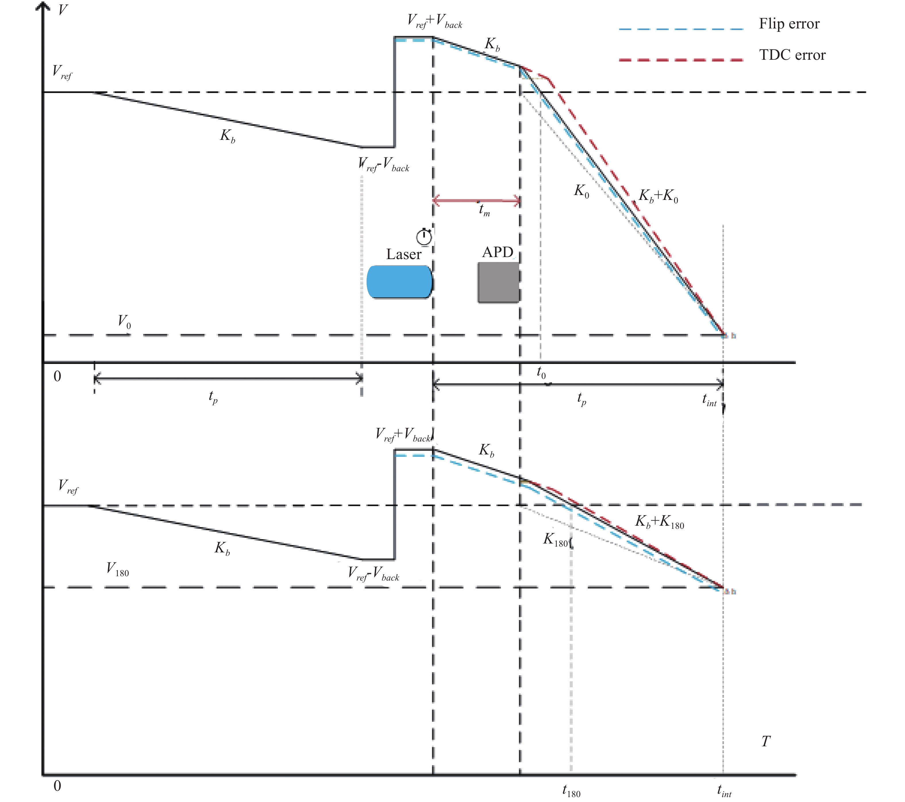
    • 为了使读出电路实现混合测距的功能并确定电路的相关参数,采用线性模式下工作的P-on-N碲镉汞APD作为探测器,建立了如图4所示的两段两相的混合测距数学模型。该模型将直接测距的原理应用于连续脉冲波,与间接测距结合并应用于背景光的情况下。

      Figure 4.  Hybrid ranging model

      混合测距模型包含0相位和180相位的积分曲线,具体参数包括:${V}_{{{ref}}}$为复位后的输出电压;${K}_{b}、 {K}_{0}、{K}_{180}$为背景光、0相位和180相位方波积分斜率;${V}_{0}、{V}_{180}$为积分结束后的输出电压;$ {t}_{m} $为求解$k $值所需要的粗测飞行时间;$ \varphi $为相位角;${t}_{0}、{t}_{180}$为计数器停止时刻;$ {t}_{int} $为积分结束时刻;$ {t}_{p} $为单段积分时间;$ {V}_{back} $为背景光在第一段积分过程中的积分电压。其中${V}_{ref}、{t}_{int}、{t}_{p}$由读出电路设置,${V}_{0}、{V}_{180}、{t}_{0}、{t}_{180}$是读出电路的输出。

      电压复位为${V}_{{{ref}}}$后,进行第一段背景光电流积分,经过$ {t}_{p} $后第一段积分结束,随后斩波电路工作,输出电压翻转。进入第二段积分,发射连续激光脉冲,计数器同步开始计数,第二段积分开始时刻仍然只有背景光积分,直到模拟脉冲被探测器接收之后产生光电流,背景光与脉冲激光同时积分。当积分电压下降到${V}_{{{ref}}}$时,计数器停止计数。选择${V}_{{{ref}}}$作为比较器阈值电压,一是由于两段积分中背景光积分电压总和为0,电路积分电压下降到${V}_{{{ref}}}$的时间必然发生在激光脉冲反射回探测器之后;二是积分时间结束后输出电压一定小于等于${V}_{{{ref}}}$,即积分过程一定经过${V}_{{{ref}}}$。两相测距的积分情况如图5所示,通过公式(8)可以实现0~$ \pi $范围内的相位测量,可表示为:

      Figure 5.  Two phase ranging

      假设计数器的计数值为${N}_{{{count}}}$,时钟周期为$ {t}_{clk} $,输出电压在第二段积分到${V}_{{{ref}}}$的时间$ {t}_{0} $,则背景光与0相位积分斜率之和为:

      背景光与180相位积分斜率之和为:

      通过斩波电路使背景光在整个过程中的总积分为0,最终的积分结果只和连续脉冲激光积分有关,通过公式(8)求出相位角,像素电路可以采用两相、四相等多个相位来测量相移,如果相移接近周期的一半,0相位和180相位的积分曲线会非常相似,产生较大的误差,此时采用更多的相位信息可以有效地解决这一问题,但这通常意味着更复杂的数据处理,因此选择测距相位数量时需要在精度、帧率、功耗等因素之间折中。公式(10)为两相测距时的情况,表示为:

      推导出0相位和180相位积分的斜率,$ {K}_{0} $、$ {K}_{180} $反映了反射激光的强度信息,模型中粗测飞行时间如公式(12)所示:

      混合测距的精度由间接测距决定,通过$ {t}_{m} $获得$ k $值,总相移为:

      式中:fix()代表向下取整;$ {f}_{m} $为调制频率。利用混合测距模型,$\mathrm{通}\mathrm{过}\mathrm{读}\mathrm{出}\mathrm{电}\mathrm{路}\mathrm{获}\mathrm{取}{V}_{0}、{V}_{180}、{t}_{0}、{t}_{180}$,相位角的范围可以扩展多个周期,同时保留了间接测距下的测距精度。

      图4中,蓝色虚线为斩波电路带来的误差Δ$ b $对混合测距模型的影响,可以看到翻转电路造成的误差不会改变飞行时间,只改变积分的输出电压,进而对间接测距造成的下式的影响:

      计数器的误差(包括计数器精度不足和比较器的传输延时)会给$ {t}_{0} $和$ {t}_{180} $造成相应的误差$ \mathrm{\Delta }{t}_{0} $和$ \mathrm{\Delta }{t}_{180} $。如图4中红色虚线所示,和斩波电路造成的误差正好相反,计数器带来的误差只会对计数器停止时刻造成相应的影响,而不会改变输出电压和间接测距的测距结果。

      根据混合测距模型可知,背景光的强度会对$ {t}_{0} $和$ {\Delta t}_{0} $造成影响,确定测距时允许的背景光强度范围是必要的,积分曲线中的斜率反映了强度的大小。使用matlab进行仿真,激光的积分强度是−2.5 V/μs (按照公式(8)设定实际平均相位脉冲积分强度与相位角的关系),在−0.005~−0.25 V/μs 的背景光积分强度下,选取100 MHz时钟频率的计数器,飞行时间选定0~800 ns的飞行时间,包含32个子周期,计算${V}_{0}、{V}_{180}、 {t}_{0}、{t}_{180}$,并按照公式(14)计算测得的飞行时间,与理想值比较,得出平均误差,仿真结果如图6所示。背景光斜率对$ {t}_{0} $的影响并非完全单向,但总体趋势是随着背景光强度的增大,误差升高。

      Figure 6.  Effect of ambient light on precision

      为了确定计数器采用的时钟频率,在背景光斜率为−0.1 V/μs时仿真,时钟频率从50~200 MHz变化,其他仿真条件不变,计算得飞行时间精度仿真曲线如图7所示,与设想相符,时钟频率越高,平均误差越小。但是时钟频率的增大意味着相同bit位数下的可测范围降低,为了保持测距的量程不变,需要更大的面积和功耗,数字输出位数的增加也会影响帧率。依据公式(14),仿真结果的平均误差仅仅能反映背景光强度和时钟频率对测距结果造成的影响,只要误差明显小于调制周期的一半,就不致于对结果的$ k $值造成影响,测距的精度仍由间接测距精度决定。根据图6图7所示,背景光积分斜率不超过−0.2 V/μs,选择100 MHz的时钟信号,计数器bit位数为8位,量程为2.56 μs,覆盖积分时间$ {t}_{p} $(1.5 μs)。

      Figure 7.  Effect of clock frequency on precision

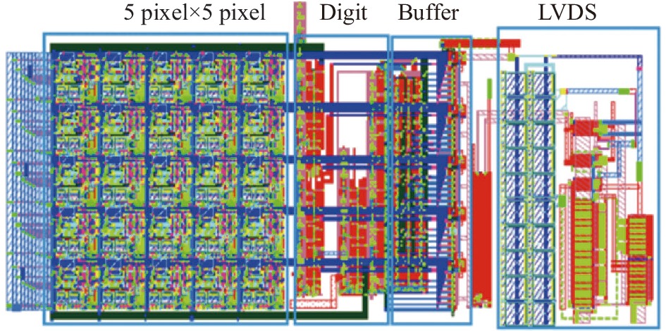
    • 基于0.18 μm SMIC 1 P6M 3.3 V工艺进行了5×5阵列电路的设计以及版图的绘制,对阵列电路进行仿真。图8所示为主要电路版图。

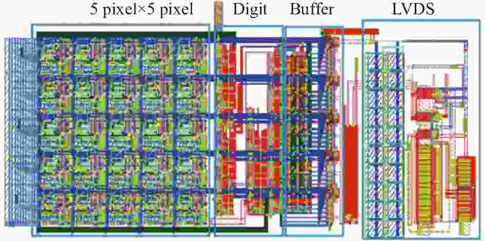
      Figure 8.  Main circuit layout

      混合测距读出电路仍然具有被动积分的功能,仿真时探测器的电阻设定为10 MΩ,电容为1 pF,调制频率为20 MHz。输出电压摆幅和线性度都会对测距的精度造成影响,选取背景光电流50 nA,0~700 nA范围内占空比为50%的连续脉冲电流,图9是线性度仿真的结果,输出范围在0.5~2.5 V,CTIA的注入效率较高,线性度达到99.83%。

      Figure 9.  Linearity test

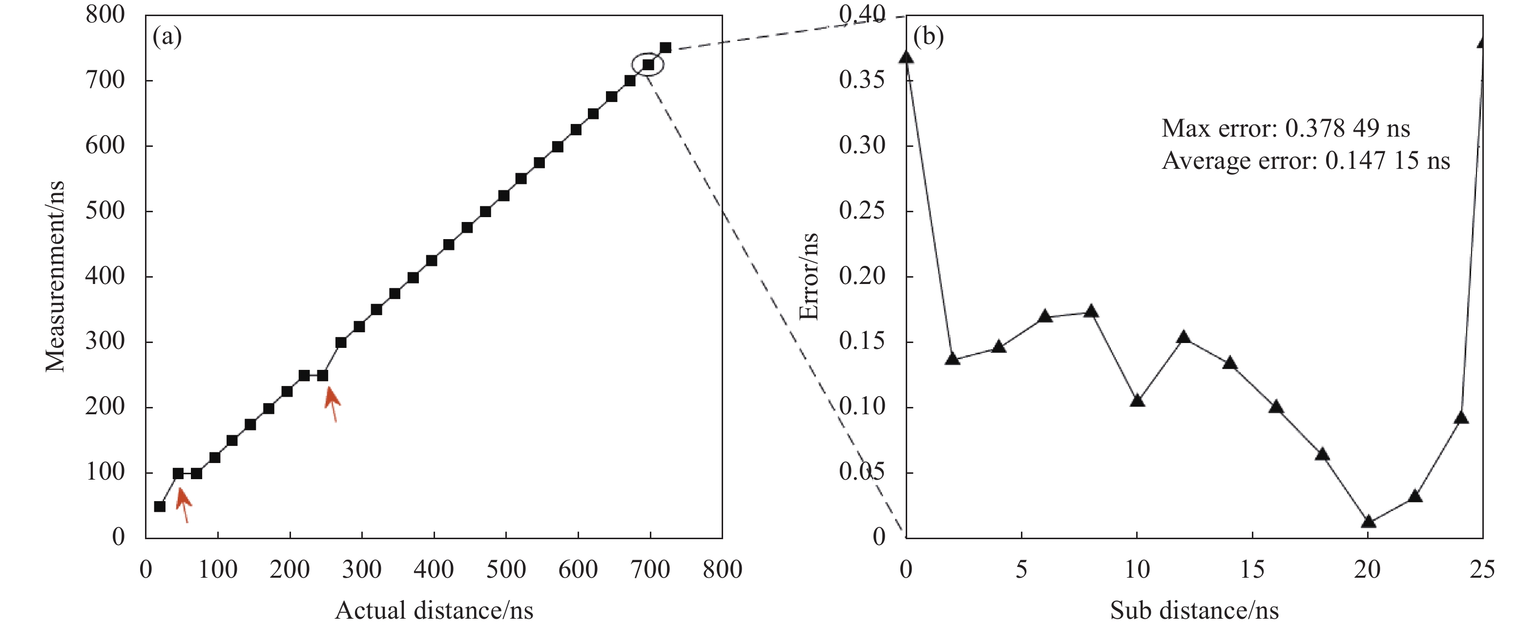
      混合测距的精度时激光电流大小为500 nA (激光电流实际平均积分斜率由相移决定),背景光电流大小为10 nA,仿真飞行时间范围从0~725 ns (0~108.75 m),共包括29个子周期,子周期范围是3.75 m,根据公式(14),利用输出电压、计数器输出结果得到测量的飞行时间,与实际值比较,得到图10。从图10(a)可以观察到,绝大多数子周期都可以正确求出k值,第2、10个子周期$k $值的误差需要通过更多相位校正。混合测距的测距范围由多个子周期组成,测距精度仍由间接测距的精度决定,由于间接测距的信噪比和积分时间成正比,最后一个子周期的误差最大,图10(b)反映了第29个子周期内的精度,最大误差出现在子周期的首末端,大小为0.378 49 ns (11.355 cm),这是由公式(8)得出,平均误差为0.147 15 ns (4.415 cm),平均误差与最大误差差别较大,这证明首末端的数据处理仍有很大优化空间。

      Figure 10.  (a) Hybrid ranging results; (b) Accuracy error of the 29th subperiod

      表1给出了读出电路的工艺条件、主要参数及性能的仿真结果,并与国内外各种测距模式下的设计进行了对比。可以看出,文中基于LM-APD的小面阵读出电路,采用中等工艺,在较低的调制频率下实现了远高于间接测距的范围,与直接测距方案相比,以极低的计数器成本实现了较高的精度,线性度良好,提供了一种可应用于近中距离的混合测距方案。

      PerformanceRef.[4]Ref.[6]Ref.[9]Ref.[10]Ref.[11]Ref.[12]Ref.[13]This paper
      TOF typeDirectDirectIndirectHybridHybridIndirectIndirectHybrid
      Technology/nm18018018065-130110180
      Resolution320×25664×6464×641200×900640$ \times $480512$ \times $42464×645×5
      Pixel size/μm305020610103250
      Input stageCTIACTIACTIADIDIDICTIACTIA
      DetectorLM-APDGM-APDPDGM-APDPD-LM-APDLM-APD
      Range/m30613.57.5250400.8-4.22108.75
      Nonlinearity-1.1%---0.75%0.2%
      Precision/cm111531.510-150402.16.811.355
      Modulation Frequency/MHz--2.55090/110802525
      Frame/fps7200002645030309666700

      Table 1.  Comparison of performance in this paper with advanced designs

    • 文中结合直接测距和间接测距的优势,建立并系统分析了混合测距模型,依据该模型可以求出飞行时间、反射回的背景光及连续脉冲光的强度。并基于此模型采用LM-APD,设计了50 μm 像素中心距的5×5阵列两段两相混合测距读出电路,一帧中包括两个相位的子帧,每个子帧又包括两个阶段的积分过程。该读出电路采用CTIA作为输入级,输出包括电压模拟输出和8 bit计数器数字输出两种。仿真结果表明在20 MHz的调制频率下,模拟输出达到了99.83%的线性度,读出电路在108.75 m的混合测距范围内达到了11.355 cm的最大误差,4.415 cm的平均误差,并将距离扩展到为纯间接测距的29倍,读出电路在精度与范围等关键性能上还有极大潜力。初步的仿真结果已经证明了混合测距的优势,验证了混合测距模型的可行性,为应用于军事或民用方面的更大规模的红外焦平面三维成像读出电路设计提供了理论和电路参考,有待于流片后进一步的验证和改进。

Reference (15)

Catalog

    /

    DownLoad:  Full-Size Img  PowerPoint
    Return
    Return