Volume 52 Issue 6
Jun.  2023
Turn off MathJax
Article Contents

Zhou Qingwei, Wu Fan, Luo Fang, Huang Xianyan, Guo Chucai, Zhu Zhihong. Control of photoelectric properties in all-inorganic CsPbBr3 thin films with two-dimensional interface modification[J]. Infrared and Laser Engineering, 2023, 52(6): 20230219. doi: 10.3788/IRLA20230219
Citation: Zhou Qingwei, Wu Fan, Luo Fang, Huang Xianyan, Guo Chucai, Zhu Zhihong. Control of photoelectric properties in all-inorganic CsPbBr3 thin films with two-dimensional interface modification[J]. Infrared and Laser Engineering, 2023, 52(6): 20230219. doi: 10.3788/IRLA20230219

Control of photoelectric properties in all-inorganic CsPbBr3 thin films with two-dimensional interface modification

doi: 10.3788/IRLA20230219
Funds:  National Natural Science Foundation of China (52101257)
  • Received Date: 2023-04-12
  • Rev Recd Date: 2023-05-15
  • Publish Date: 2023-06-25
  •   Objective  As a new generation photovoltaic technology, perovskite solar cells (PSCs) have achieved a comparable efficiency to commercial silicon-based solar cells, demonstrating great application potential. However, these photoactive layers based on organic-inorganic hybrid perovskites are very unstable, which seriously hinders their commercial application. Therefore, all-inorganic CsPbBr3 perovskite has attracted enormous attention due to its outstanding environmental tolerance to heat, moisture, oxygen and UV light. Unfortunately, the device efficiency based on CsPbBr3 perovskite is relatively lower compared to that of the PSCs device with organic-inorganic hybrid perovskites. The recombination of charge carriers at the interface between the charge transport layers and the perovskite layer in all-inorganic CsPbBr3 PSCs is the key factor that restricts the further improvement of its photoelectric conversion efficiency (PCE). In recent years, two-dimensional transition metal dichalcogenides (TMDCs) materials represented by MoS2, MoSe2, WS2 and WSe2 have attracted more and more attention due to their unique physical and chemical properties. With the advantages such as adjustable band gap and band edge, high carrier mobility, stable chemical properties and matching energy level with perovskite materials, two-dimensional TMDCs are regarded as effective interface modification materials to promote interface charge extraction in all inorganic CsPbBr3 PSCs. However, the current research on using two-dimensional materials as interface modification layers and charge carrier transport layers in all-inorganic PSC is still in its infancy.   Methods  Through interface engineering, various two-dimensional TMDCs (MoS2, MoSe2, WS2, and WSe2) materials are introduced at the interface between the perovskite layer and the electron transport layer of the all-inorganic CsPbBr3 PSCs with an FTO/SnO2/TMDCs/CsPbBr3/C structure. The two-dimensional TMDCs here act as both interface modification materials and carrier transport layers. Through interface level compensation and barrier reduction with TMDCs interlayers, the carrier extraction and transport in all-inorganic CsPbBr3 PSC devices are promoted (Fig.1). Moreover, by constructing TMDCs/CsPbBr3 van der Waals heterostructure, high-quality CsPbBr3 perovskite thin films with large and compact grains are grown via lattice matched van der Waals epitaxy (Fig.5).   Results and Discussions  The interface charge loss between the perovskite layer and the electron transport layer is reduced, and the carrier extraction in the all-inorganic CsPbBr3 PSC devices are enhanced, so that the PCE of the devices is increased from the initial 7.94% to 10.02%, and the open-circuit voltage is increased from 1.474 V to 1.567 V (Fig.8). In addition, Mott–Schottky curves are measured in the dark by performing capacitance-voltage characterization, which demonstrates an enhanced built-in potential, indicating the enlarged driving force for charge transportation with TMDCs/CsPbBr3 heterostructure (Fig.9). Finally, the time-resolved photoluminescence decay measurements are performed to investigate the photoluminescence decay lifetimes, which are closely related to the electron extraction ability. Due to better energy level matching of TMDCs with perovskite layers, CsPbBr3 perovskite layers show shorter carrier lifetimes on TMDCs interlayer (Fig.10), which further confirms the enhanced electron extraction ability from perovskite to the electron transport layer.   Conclusions  A novel strategy is developed to prepare high-quality perovskite films by constructing TMDCs/CsPbBr3 van der Waals heterostructure and achieve high-performance photoelectric devices through interfacial energy level matching, which provides a new way for the development of all-inorganic perovskite optoelectronic devices based on two-dimensional TMDCs materials.
  • [1] Wu C, Fang W, Cheng Q, et al. MXene-regulated perovskite vertical growth for high-performance solar cells [J]. Angewandte Chemie International Edition, 2022, 61(43): e202210970. doi:  https://doi.org/10.1002/anie.202210970
    [2] Wang Z, Shi Z, Li T, et al. Stability of perovskite solar cells: a prospective on the substitution of the a cation and X anion [J]. Angewandte Chemie International Edition, 2017, 56(5): 1190-1212. doi:  10.1002/anie.201603694
    [3] Zhang J, Hodes G, Jin Z, et al. All-inorganic CsPbX3 perovskite solar cells: progress and prospects [J]. Angewandte Chemie International Edition, 2019, 58(44): 15596-15618. doi:  10.1002/anie.201901081
    [4] Liang J, Wang C, Wang Y, et al. All-inorganic perovskite solar cells [J]. Journal of the American Chemical Society, 2016, 138(49): 15829-15832. doi:  10.1021/jacs.6b10227
    [5] Zhou Q, Du J, Duan J, et al. Photoactivated transition metal dichalcogenides to boost electron extraction for all-inorganic tri-brominated planar perovskite solar cells [J]. Journal of Materials Chemistry A, 2020, 8(16): 7784-7791. doi:  10.1039/D0TA01645D
    [6] 陈红富, 罗曼, 沈倪明, 等. 二维层状材料异质结光电探测器研究进展 (特邀) [J]. 红外与激光工程, 2021, 50(1): 20211018. doi:  10.3788/IRLA20211018

    Chen Hongfu, Luo Man, Shen Niming, et al. Research progress of two-dimensional layered materials-based heterojunction photodetectors (Invited) [J]. Infrared and Laser Engineering, 2021, 50(1): 20211018. (in Chinese) doi:  10.3788/IRLA20211018
    [7] 王奕方, 吴侃, 陈建平. MoS2/WSe2-PVA 薄膜热光全光调制器(特邀) [J]. 红外与激光工程, 2019, 48(1): 0103003. doi:  10.3788/IRLA201948.0103003

    Wang Yifang, Wu Kan, Chen Jianping. All-optical thermal modulator based on MoS2/WSe2-PVA thin film (invited) [J]. Infrared and Laser Engineering, 2019, 48(1): 0103003. (in Chinese) doi:  10.3788/IRLA201948.0103003
    [8] Anasori B, Lukatskaya M R, Gogotsi Y. 2D metal carbides and nitrides (MXenes) for energy storage [J]. Nature Reviews Materials, 2017, 2(2): 16098. doi:  10.1038/natrevmats.2016.98
    [9] Bati A S R, Batmunkh M, Shapter J G. Emerging 2D layered materials for perovskite solar cells [J]. Advanced Energy Materials, 2020, 10(13): 1902253. doi:  10.1002/aenm.201902253
    [10] Yang G, Chen C, Yao F, et al. Effective carrier-concentration tuning of SnO2 quantum dot electron-selective layers for high-performance planar perovskite solar cells [J]. Advanced Materials, 2018, 30(14): 1706023. doi:  10.1002/adma.201706023
    [11] Kang J, Tongay S, Zhou J, et al. Band offsets and hetero-structures of two-dimensional semiconductors [J]. Applied Physics Letters, 2013, 102(1): 012111. doi:  10.1063/1.4774090
    [12] Zhou Q, Duan J, Wang Y, et al. Tri-functionalized TiOxCl4-2x accessory layer to boost efficiency of hole-free, all-inorganic perovskite solar cells [J]. Journal of Energy Chemistry, 2020, 50: 1-8. doi:  10.1016/j.jechem.2020.03.004
    [13] Voiry D, Yamaguchi H, Li J, et al. Enhanced catalytic activity in strained chemically exfoliated WS2 nanosheets for hydrogen evolution [J]. Nature Materials, 2013, 12(9): 850-855. doi:  10.1038/nmat3700
    [14] Yang T, Zheng B, Wang Z, et al. Van der Waals epitaxial growth and optoelectronics of large-scale WSe2/SnS2 vertical bilayer p–n junctions [J]. Nature Communications, 2017, 8(1): 1906. doi:  10.1038/s41467-017-02093-z
    [15] Chen X, Liu G, Zheng W, et al. Vertical 2D MoO2/MoSe2 core-shell nanosheet arrays as high-performance electrocatalysts for hydrogen evolution reaction [J]. Advanced Functional Materials, 2016, 26(46): 8537-8544. doi:  10.1002/adfm.201603674
    [16] Zhou Q, Su S, Cheng P, et al. Robust ferromagnetism in zigzag-edge rich MoS2 pyramids [J]. Nanoscale, 2018, 10(24): 11578-11584. doi:  10.1039/C8NR03038C
    [17] Zhao Y, Duan J, Wang Y, et al. Precise stress control of inorganic perovskite films for carbon-based solar cells with an ultrahigh voltage of 1.622 V [J]. Nano Energy, 2020, 67: 104286. doi:  10.1016/j.nanoen.2019.104286
    [18] Tang G, You P, Tai Q, et al. Solution-phase epitaxial growth of perovskite films on 2D material flakes for high-performance solar cells [J]. Advanced Materials, 2019, 31(24): 1807689. doi:  https://doi.org/10.1002/adma.201807689
    [19] Yan L, Xue Q, Liu M, et al. Interface engineering for all-inorganic CsPbI2Br perovskite solar cells with efficiency over 14% [J]. Advanced Materials, 2018, 30(33): 1802509. doi:  10.1002/adma.201802509
    [20] Liu Z, Chang J, Lin Z, et al. High-performance planar perovskite solar cells using low temperature, solution-combustion-based nickel oxide hole transporting layer with efficiency exceeding 20% [J]. Advanced Energy Materials, 2018, 8(19): 1703432. doi:  10.1002/aenm.201703432
    [21] Liu Y, He B, Duan J, et al. Poly(3-hexylthiophene)/zinc phthalocyanine composites for advanced interface engineering of 10.03%-efficiency CsPbBr3 perovskite solar cells [J]. Journal of Materials Chemistry A, 2019, 7(20): 12635-12644. doi:  10.1039/C9TA01151J
    [22] Chen W, Wu Y, Yue Y, et al. Efficient and stable large-area perovskite solar cells with inorganic charge extraction layers [J]. Science, 2015, 350(6263): 944-948. doi:  10.1126/science.aad1015
    [23] Duan J, Zhao Y, Yang X, et al. Lanthanide ions doped CsPbBr3 halides for HTM-free 10.14%-efficiency inorganic perovskite solar cell with an ultrahigh open-circuit voltage of 1.594 V [J]. Advanced Energy Materials, 2018, 8(31): 1802346. doi:  10.1002/aenm.201802346
  • 加载中
通讯作者: 陈斌, bchen63@163.com
  • 1. 

    沈阳化工大学材料科学与工程学院 沈阳 110142

  1. 本站搜索
  2. 百度学术搜索
  3. 万方数据库搜索
  4. CNKI搜索

Figures(10)  / Tables(2)

Article Metrics

Article views(137) PDF downloads(26) Cited by()

Related
Proportional views

Control of photoelectric properties in all-inorganic CsPbBr3 thin films with two-dimensional interface modification

doi: 10.3788/IRLA20230219
  • 1. College of Advanced Interdisciplinary Studies & Hunan Provincial Key Laboratory of Novel Nano-Optoelectronic Information Materials and Devices, National University of Defense Technology, Changsha 410073, China
  • 2. Nanhu Laser Laboratory, National University of Defense Technology, Changsha 410073, China
Fund Project:  National Natural Science Foundation of China (52101257)

Abstract:   Objective  As a new generation photovoltaic technology, perovskite solar cells (PSCs) have achieved a comparable efficiency to commercial silicon-based solar cells, demonstrating great application potential. However, these photoactive layers based on organic-inorganic hybrid perovskites are very unstable, which seriously hinders their commercial application. Therefore, all-inorganic CsPbBr3 perovskite has attracted enormous attention due to its outstanding environmental tolerance to heat, moisture, oxygen and UV light. Unfortunately, the device efficiency based on CsPbBr3 perovskite is relatively lower compared to that of the PSCs device with organic-inorganic hybrid perovskites. The recombination of charge carriers at the interface between the charge transport layers and the perovskite layer in all-inorganic CsPbBr3 PSCs is the key factor that restricts the further improvement of its photoelectric conversion efficiency (PCE). In recent years, two-dimensional transition metal dichalcogenides (TMDCs) materials represented by MoS2, MoSe2, WS2 and WSe2 have attracted more and more attention due to their unique physical and chemical properties. With the advantages such as adjustable band gap and band edge, high carrier mobility, stable chemical properties and matching energy level with perovskite materials, two-dimensional TMDCs are regarded as effective interface modification materials to promote interface charge extraction in all inorganic CsPbBr3 PSCs. However, the current research on using two-dimensional materials as interface modification layers and charge carrier transport layers in all-inorganic PSC is still in its infancy.   Methods  Through interface engineering, various two-dimensional TMDCs (MoS2, MoSe2, WS2, and WSe2) materials are introduced at the interface between the perovskite layer and the electron transport layer of the all-inorganic CsPbBr3 PSCs with an FTO/SnO2/TMDCs/CsPbBr3/C structure. The two-dimensional TMDCs here act as both interface modification materials and carrier transport layers. Through interface level compensation and barrier reduction with TMDCs interlayers, the carrier extraction and transport in all-inorganic CsPbBr3 PSC devices are promoted (Fig.1). Moreover, by constructing TMDCs/CsPbBr3 van der Waals heterostructure, high-quality CsPbBr3 perovskite thin films with large and compact grains are grown via lattice matched van der Waals epitaxy (Fig.5).   Results and Discussions  The interface charge loss between the perovskite layer and the electron transport layer is reduced, and the carrier extraction in the all-inorganic CsPbBr3 PSC devices are enhanced, so that the PCE of the devices is increased from the initial 7.94% to 10.02%, and the open-circuit voltage is increased from 1.474 V to 1.567 V (Fig.8). In addition, Mott–Schottky curves are measured in the dark by performing capacitance-voltage characterization, which demonstrates an enhanced built-in potential, indicating the enlarged driving force for charge transportation with TMDCs/CsPbBr3 heterostructure (Fig.9). Finally, the time-resolved photoluminescence decay measurements are performed to investigate the photoluminescence decay lifetimes, which are closely related to the electron extraction ability. Due to better energy level matching of TMDCs with perovskite layers, CsPbBr3 perovskite layers show shorter carrier lifetimes on TMDCs interlayer (Fig.10), which further confirms the enhanced electron extraction ability from perovskite to the electron transport layer.   Conclusions  A novel strategy is developed to prepare high-quality perovskite films by constructing TMDCs/CsPbBr3 van der Waals heterostructure and achieve high-performance photoelectric devices through interfacial energy level matching, which provides a new way for the development of all-inorganic perovskite optoelectronic devices based on two-dimensional TMDCs materials.

    • 作为最有前途的新一代光伏技术之一,钙钛矿太阳能电池(PSCs)已经实现了25.7%的认证光电转换效率,与商用的硅基太阳能电池相当[1]。然而,这种基于有机-无机杂化钙钛矿的光活性层非常不稳定,严重阻碍了器件的商业化应用[2]。为此,人们通过无机Cs+离子取代有机MA+或FA+离子制备以无机钙钛矿吸光材料CsPbI3-xBrxx = 0~3)为基础的全无机钙钛矿太阳能电池,不仅提升了器件的环境稳定性,又降低了实际生产的难度和成本[3]。在这些无机的钙钛矿材料中,三溴化的CsPbBr3钙钛矿具有2.3 eV的宽带隙,同时还有最佳的耐热、耐湿、耐氧和耐紫外光的环境耐受性,因此,在串联和半透明太阳能电池中具有很大的应用潜力[4]。随着无机钙钛矿薄膜制备工艺、组分工程、界面工程、光谱工程等方法的迅速发展,全无机CsPbBr3 PSC器件的光电转换效率(PCE)已经由最初的5.92%提升至当前的超过10% [5]。然而,全无机CsPbBr3 PSC由于界面势垒过高使载流子在界面处的提取过程缓慢导致复合严重,严重制约其效率的进一步提升,因此如何优化界面材料促进界面电荷提取是提高该CsPbBr3 PSC综合性能的重要研究方向。

      近年来,以MoS2、MoSe2、WS2和WSe2等为代表的二维过渡金属硫族化合物(TMDCs)材料由于其独特的物理和化学性质受到了越来越多的关注[6-7]。二维TMDCs材料由于量子限域效应和边界效应拥有可调控的能带结构,且其载流子迁移率高、化学结构稳定、制备工艺简单[8]。此外,由于具备与钙钛矿材料匹配的能级结构,二维TMDCs材料既可以作为电子给体又可以作为电子受体,这使得其在作为界面修饰材料降低电子传输层(ETL)/钙钛矿层和钙钛矿层/空穴传输层(HTL)界面的势垒、实现能级补偿和抑制界面电荷复合等方面具有重要的应用前景[9]。然而,目前采用二维材料作为界面修饰层和载流子传输层降低全无机PSC界面势垒和提高界面电荷提取的研究仍处于起步阶段,相关基础理论问题和改进途径仍有待深入研究,如何有效地控制结构和形貌以调控其物理化学性能是二维材料作为高效界面修饰层和载流子传输层的关键。

      文中通过界面工程,将不同的二维TMDCs (MoS2、MoSe2、WS2和WSe2)材料应用到全无机CsPbBr3 PSCs器件的ETL与钙钛矿界面作为界面修饰层和载流子传输层,制备了结构为FTO/SnO2/TMDCs/CsPbBr3/C的全无机PSC器件。通过构建TMDCs/CsPbBr3范德华异质结,利用二维TMDCs与CsPbBr3的晶格匹配生长高质量的钙钛矿薄膜,同时利用TMDCs与钙钛矿的能级匹配效应,促进器件界面的载流子分离与传输并提高器件光电性能,使器件PCE由初始的7.94%提高到10.02%,为发展基于二维TMDCs材料的全无机钙钛矿光电器件提供了一个新的途径。

    • 文中实验使用的材料和试剂如下:二水合氯化亚锡(SnCl2·2 H2O, Alfa Aesar)、硫脲(CH4N2S, Macklin)、MoS2粉末(Aladdin)、MoSe2粉末(Aladdin)、WS2粉末(Aladdin)、WSe2粉末(Aladdin)、溴化铅(PbBr2,Aladdin)、溴化铯(CsBr,Aladdin)、异丙醇(IPA,Aladdin)、N,N二甲基甲酰胺(N,N-dimethylformamide,DMF,国药)、甲醇(CH3OH,国药)、导电玻璃(FTO,12 Ω □−1)、盐酸、Zn粉、乙醇、碳浆料(上海MaterWin新材料有限公司)。实验中所有材料和试剂均为原样使用,无进一步纯化。

    • SnO2量子点(QD)制备方法参考文献[10],具体过程如下:将1.015 g SnCl2·2 H2O和338 mg CH4N2S边搅拌边加入烧杯,溶解于30 mL去离子水中,接着于室温下连续敞口剧烈搅拌36 h后,得到带有SnO2 QD的黄色乳状悬浮液。然后将悬浮液以9000 rpm离心5 min,形成黄色透明的SnO2 QD溶液。获得的SnO2 QD溶液用0.22 μm聚四氟乙烯(PTFE)过滤器过滤后使用。

    • 实验采用超声剥离法制备二维TMDCs纳米片:取60 mg不同的TMDCs (MoS2、MoSe2、WS2和WSe2)粉末分别添加到100 mL IPA中,然后用超声清洗机在300 W功率下超声处理10 h;将超声处理后的溶液静置24 h后取上层悬浮液以3500 rpm转速离心30 min,分离出未剥离的TMDCs粉末沉积物,得到上层的TMDCs纳米片悬浊液;最后通过真空干燥将TMDCs纳米片悬浊液的浓度控制为0.1 mg/mL。

    • 实验采用旋涂法制备结构如图1(a)所示的全无机CsPbBr3 PSC器件。

      Figure 1.  Schematic diagrams of an all-inorganic CsPbBr3 PSC with TMDCs interlayer. Schematic diagrams of (a) device structure and (b) energy levels of different layers in the PSC device

      器件制备方法如下:先将FTO玻璃用Zn粉和盐酸在其上刻蚀出需要的电极图案,然后依次用去污剂、去离子水和乙醇超声清洗。接着将清洗干净并烘干的FTO衬底放入等离子清洗机中清洗5 min,然后在其上旋涂SnO2 QDs溶液制备电子传输层。旋涂SnO2 QDs溶液前先将FTO衬底和SnO2 QDs溶液放在80 ℃热台上预热5 min,然后在预热后的FTO衬底上旋涂SnO2 QDs溶液,旋涂条件:转速2 000 rpm时间30 s (下文中的旋涂过程均为此条件)。将旋涂好SnO2的FTO玻璃(FTO/SnO2)放在热台上在空气中加热到200 ℃退火1 h。接着将退火后的FTO/SnO2衬底冷却到室温,然后在其上旋涂TMDCs/IPA溶液,旋涂后在100 ℃的热台上加热5 min,得到FTO/SnO2/TMDCs光阳极。接着利用多步旋涂法在其上沉积CsPbBr3钙钛矿薄膜:先将FTO/SnO2/TMDCs光阳极和1 M PbBr2/DMF溶液在100 ℃热台上预热5 min,然后在FTO/SnO2/TMDCs上旋涂PbBr2/DMF溶液,再将其转移到100 ℃热台上退火30 min;接着在室温下旋涂0.07 M CsBr/CH3OH溶液后将样品放在250 ℃热台上退火5 min,多次重复旋涂CsBr/CH3OH溶液的步骤直到得到高质量的CsPbBr3钙钛矿薄膜。最后,通过刮涂法将导电碳电极涂覆在钙钛矿膜上,得到结构为FTO/SnO2/TMDCs/CsPbBr3/C的全无机钙钛矿太阳能电池。二维TMDCs能与CsPbBr3形成良好的能级匹配[11-12],如图1(b)所示,从而实现电子的高效提取。

    • 实验通过扫描电子显微镜(SEM, Hitachi S4800)、透射电子显微镜(TEM,Tecnai G2 F20)、紫外-可见光分光光度仪(Metash UV-8000 A)和X射线衍射(XRD,Bruker D8 Advance)表征样品的形貌、结构、透光性和成分组成等。太阳能电池器件测试采用的光源为AM 1.5 G模拟太阳光(Newport,Oriel Class A,91195 A),光强为100 mW/cm2(标准晶硅太阳能电池校准),测试设备为电化学工作站(CHI660 E)。使用Horiba光谱仪(激发波长为500 nm)获得样品的时间分辨的光致发光(TRPL)衰减曲线。

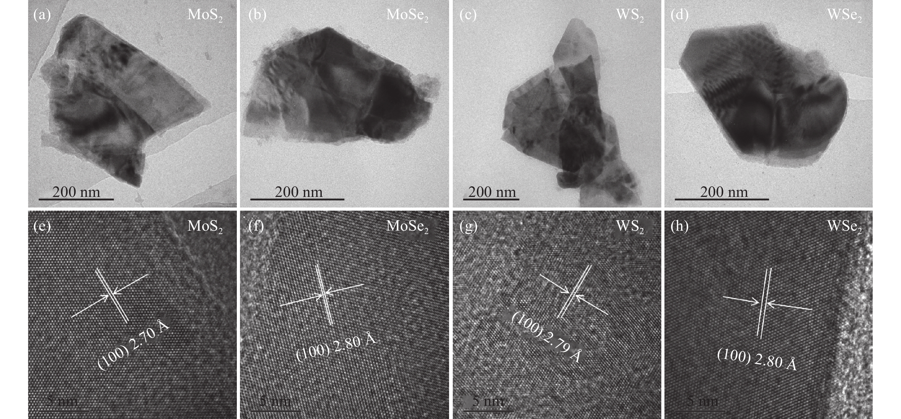
    • 为了更好地了解实验制备的不同TMDCs纳米片的晶体质量与结构以及TMDCs/CsPbBr3范德华异质结构的生长机理,文中利用TEM表征了TMDCs纳米片的形貌与结构。如图2(a)~(d)所示,通过液相剥离得到二维TMDCs成薄片状的结构。MoS2、MoSe2、WS2和WSe2纳米片的高分辨TEM(HRTEM)图像都呈现出有序的原子矩阵和清晰的晶格条纹(图2(e)~(f)),这都表明文中实验制备出了高质量的TMDCs纳米薄片。此外,从它们的HRTEM图像可以看出,MoS2、MoSe2、WS2和WSe2纳米片的(100)晶面的晶面距分别为2.70 Å、2.80 Å、2.79 Å和2.80 Å(1 Å=0.1 nm),这与以前的文献报道是一致的[1316]

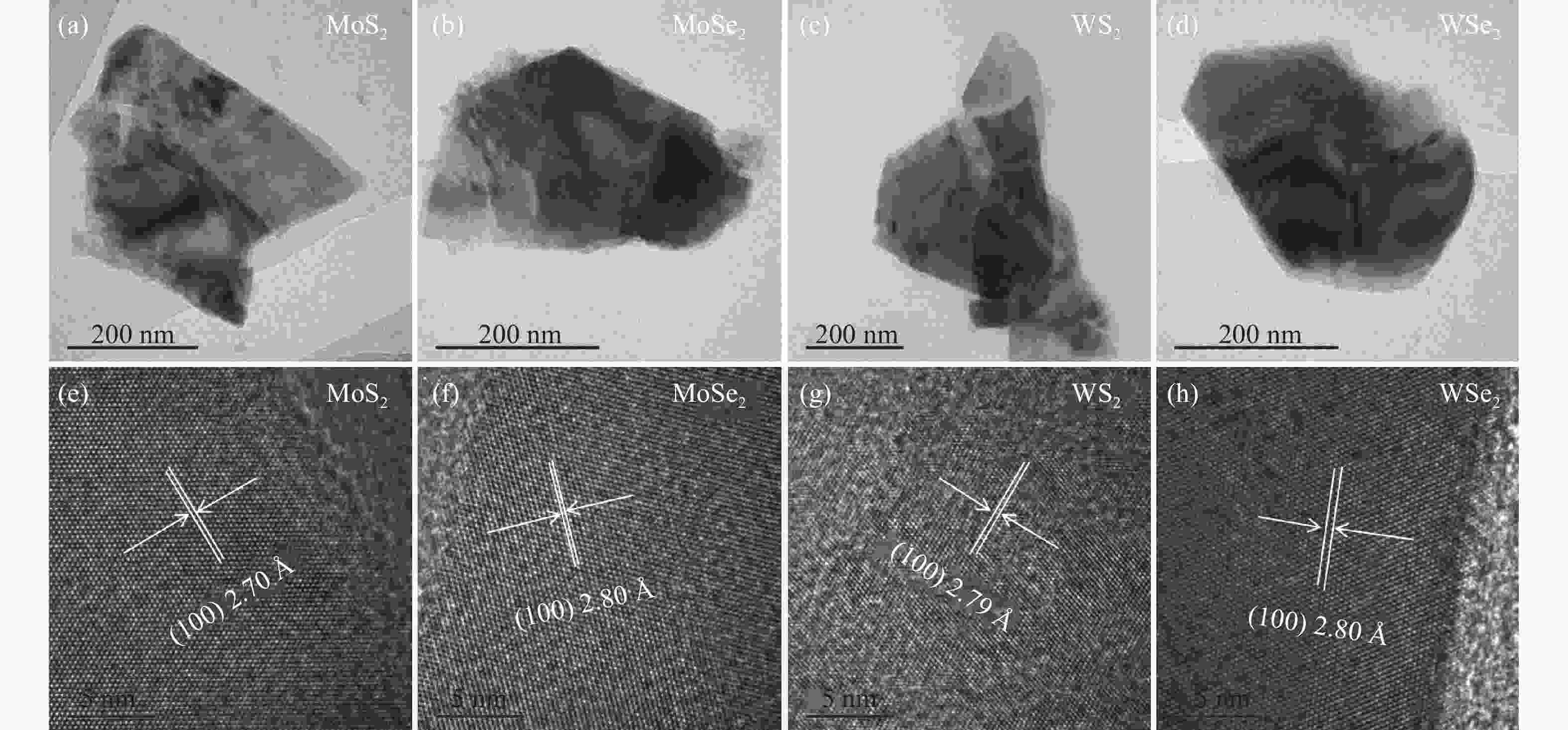
      Figure 2.  TEM and HRTEM image of TMDCs nanoflakes. (a)-(d) TEM pictures and (e)-(f) HRTEM pictures for (a), (e) MoS2 nanoflake, (b), (f) MoSe2 nanoflake, (c), (g) WS2 nanoflake, (d), (h) WSe2 nanoflake

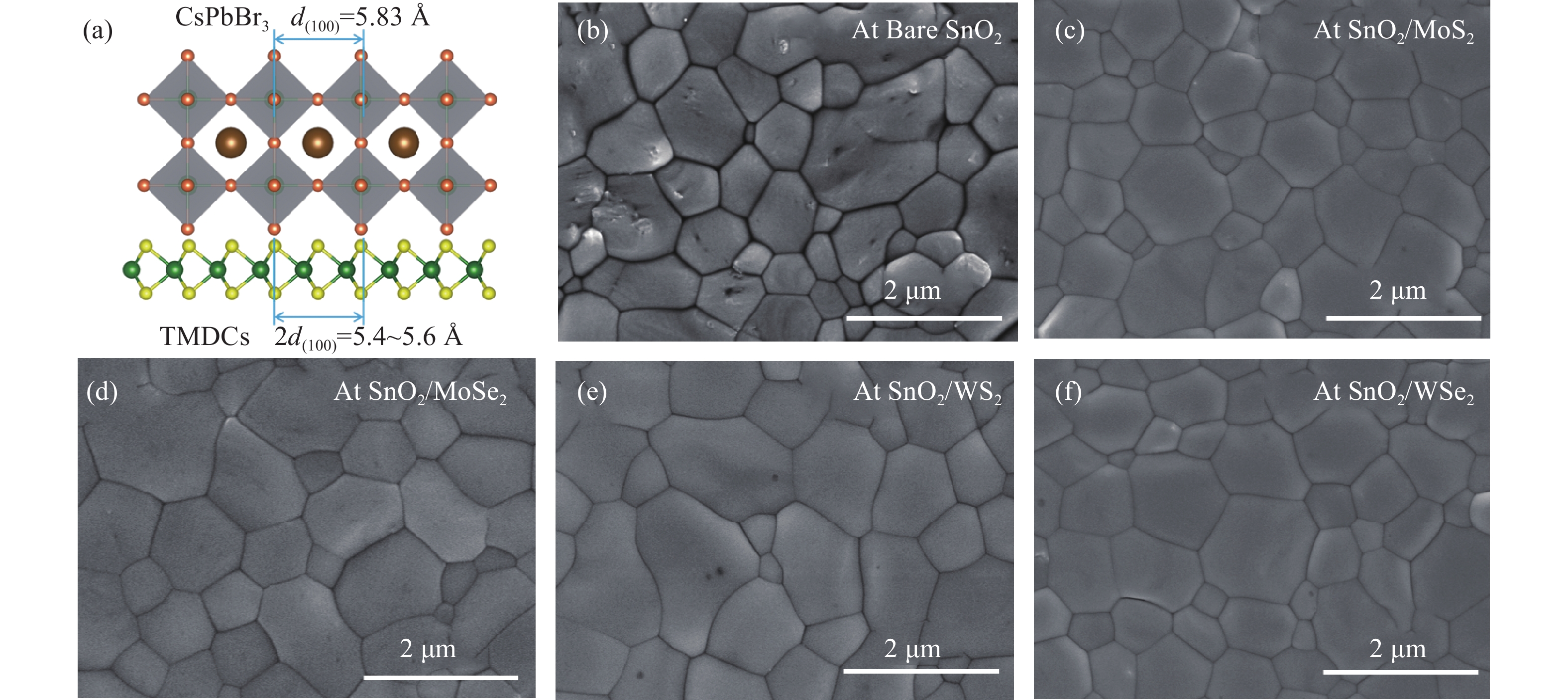
      为了研究CsPbBr3钙钛矿薄膜在TMDCs纳米片修饰的SnO2表面上的形貌演变,首先观察了不同ETL基底的表面形貌。图3为不同放大倍数的SnO2基底、SnO2/MoS2基底、SnO2/MoSe2基底、SnO2/WS2基底以及SnO2/WSe2基底的SEM图像。通过对不同TMDCs修饰后的基底对应的SEM图像与未修饰的基底对比可以看出,TMDCs纳米薄片修饰后基底表面更平滑且TMDCs分布均匀,这无疑有利于生长高质量的钙钛矿薄膜。此外,利用紫外-可见光分光光度仪测试了不同TMDCs修饰的基底在200~1100 nm波段的透过率。测试时首先将紫外-可见光分光光度仪在不放基底的情况下进行基线校准,然后放入不同的基底,分别测得其透过率曲线(图4)。对比未修饰的SnO2基底和不同TMDCs修饰的基底在可见光波段的透过率曲线可以看出,TMDCs修饰对基底的透过率影响不大。

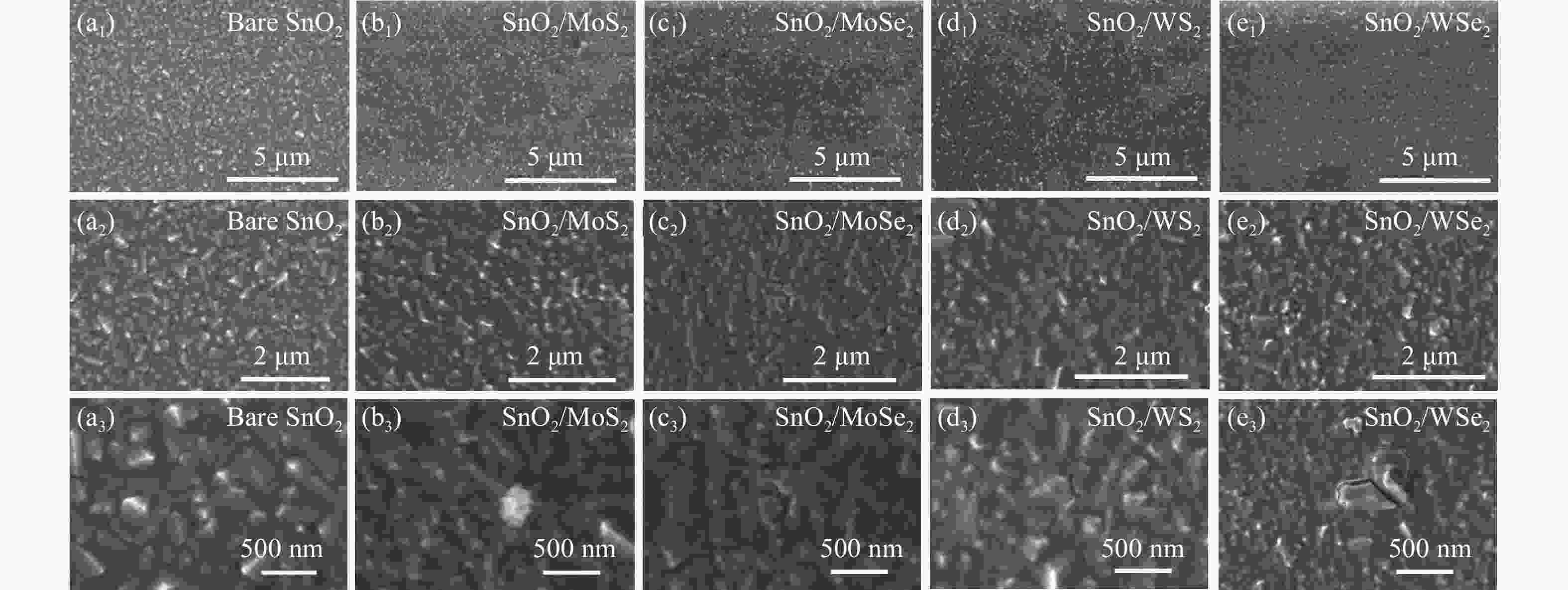
      Figure 3.  Top-view SEM images of the SnO2 films with TMDCs modification. Top-view SEM images of the films with different magnifications, (a1)-(a3) bare SnO2, (b1)-(b3) SnO2/MoS2, (c1)-(c3) SnO2/MoSe2, (d1)-(d3) SnO2/WS2 and (e1)-(e3) SnO2/WSe2

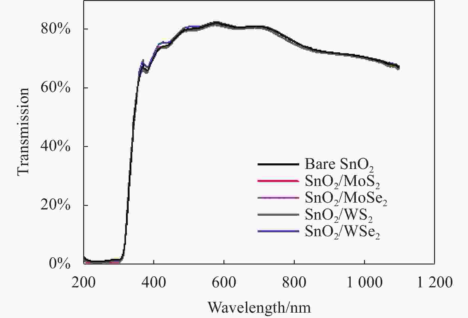
      Figure 4.  Transmission curves of FTO/ETL substrates with different TMDCs modification at visible wavelengths

      接着,研究分析了CsPbBr3钙钛矿薄膜在TMDCs上的生长机理。如图5(a)所示,CsPbBr3立方晶体中(100)平面的晶面距为5.83 Å(PDF#54–0752)[17],非常接近TMDCs的(100)晶面距的两倍(5.4~5.6 Å),这就使CsPbBr3晶体能在TMDCs纳米片上沿(100)方向自发外延生长[18]。因此,由于异质结界面处范德华相互作用的存在,CsPbBr3晶粒的生长过程将受到调控。钙钛矿前驱体在旋涂到TMDCs表面后,由于Pb和S、Se原子之间的相互作用,将实现自组装过程。CsPbBr3和TMDCs之间的面内范德华力耦合作用以及TMDCs无悬空键的(100)晶面为CsPbBr3在其上的面外取向生长提供了一个出色的模板,同时促进CsPbBr3形成大尺寸晶粒,并降低缺陷密度[18]

      Figure 5.  Schematic diagram and SEM images of CsPbBr3 perovskite grown on TMDCs. (a) Schematic diagram of CsPbBr3 perovskite grown on TMDCs; Top-view SEM images of CsPbBr3 perovskite films grown at the surface of (b) bare SnO2, (c) SnO2/MoS2, (d) SnO2/MoSe2, (e) SnO2/WS2 and (f) SnO2/WSe2

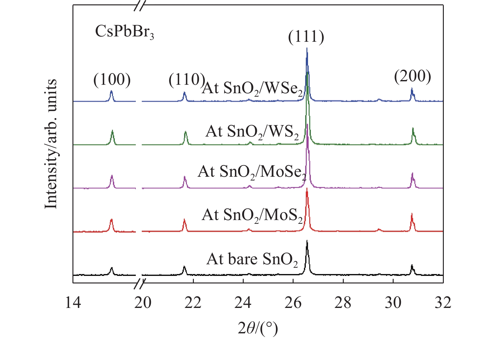
      图5(b)~(f)是在不同基底上生长的CsPbBr3钙钛矿薄膜的俯视SEM图像。如图所示,无论是否有TM-DCs中间层,CsPbBr3薄膜都能均匀地覆盖住其下的ETL,没有任何针孔。仔细观察后可以发现,相对于对照组,在TMDCs上生长的CsPbBr3薄膜表现出明显的晶粒尺寸增大、晶界少、裂纹减少的现象,并且晶粒之间更加紧实,这表明TMDCs中间层在调节CsPbBr3结晶动力学方面具有积极作用。从CsPbBr3薄膜的XRD图也可以看出(图6),不同TMDCs修饰后的钙钛矿的(111)晶面的特征峰强度均明显增加,表明TMDCs中间层的界面调节促进了钙钛矿薄膜(111)晶面的生长,使其薄膜晶体质量得到改善。而良好的薄膜晶体质量可以降低钙钛矿层中的电荷陷阱密度,从而增强器件的光伏性能。

      Figure 6.  XRD patterns of the CsPbBr3 perovskite films grown at different surfaces

      基于TMDCs优化的ETL界面,文中进一步评估了TMDCs中间层对全无机CsPbBr3 PSC光伏性能的影响。如图7所示,典型的全无机CsPbBr3 PSC器件结构为FTO/SnO2/TMDCs/CsPbBr3/C,包含FTO层、SnO2/TMDCs层(厚约60 nm)、CsPbBr3钙钛矿层(厚约500 nm)和碳电极层等。

      Figure 7.  Cross-sectional SEM image of an all-inorganic CsPbBr3 PSC with TMDCs interlayer

      由于TMDCs层的导带底的位置在SnO2层和钙钛矿层的导带底之间,因此可以形成中间能级,减小层间的能级差,从而提高了界面电子的提取效率[19]。文中在模拟阳光下(AM1.5,100 mW/cm2)测试了TM-DCs修饰前后的全无机PSC的光伏性能。图8(a)是不同TMDCs界面修饰器件在光照下的电流-电压(J-V)曲线,表1列出了不同器件的PCE、开路电压(Voc)、短路电流密度(Jsc)和填充因子(FF)等光伏数据。相比于未修饰的原始器件,不同TMDCs修饰后的器件效率均有提升,最高达到10.02%(WS2),远高于原始器件的7.94%效率。器件效率的提高主要得益于TMDCs界面调节后JscVoc的显著提高,它们分别从原始器件的7.01 mA/cm2和1.474 V提高到界面调节后的7.97 mA/cm2和1.567 V。TMDCs修饰后器件性能的提升主要是由于修饰后钙钛矿薄膜质量的提升以及界面势垒的降低,减少了界面缺陷态密度,促进了载流子的分离与传输。为了进一步验证J-V测试的可靠性,在器件最大功率点的偏置电压下表征了其稳态功率输出。如图8(b)所示,与原始器件相比,经过TMDCs优化后的器件的效率均有明显增强,结果与J-V测量一致。此外,TMDCs/CsPbBr3范德华异质结的形成可以降低界面势垒,同时引导晶格重构,减少钙钛矿薄膜中的缺陷,加速电荷的提取和转移,这些都有利于减小器件正反扫迟滞。如图8(c)所示,WS2修饰后的器件的迟滞现象相比于原始器件明显减弱,修饰后的器件的迟滞因子从原始器件的32.4%减少到24.3%。最后,在温度为25 ℃,湿度为80%的环境条件下评估了器件的稳定性。如图8(d)所示,没有封装的FTO/SnO2/WS2/CsPbBr3/C器件的VocJsc、PCE和FF在存储17天后可以保持初始值的90%以上。这种出色的器件稳定性除了是由于全无机CsPb-Br3钙钛矿本身的高稳定性外,还归因于其器件顶部碳电极层提供的额外的耐湿性。

      Figure 8.  Photovoltaic performance of the PSCs with and without TMDCs modification. (a) JV curves and (b) steady power output curves of different devices; (c) J-V curves of the pristine device and the device with WS2 modification under forward and reverse scan directions; (d) Normalized Voc, Jsc, PCE and FF stability curves of FTO/SnO2/WS2/CsPbBr3/C device under 25 °C and 80% humidity condition

      All-inorganic PSC devicesVoc/VJsc/mA·cm−2PCEFF
      FTO/SnO2/CsPbBr3/C1.4747.017.94%76.9%
      FTO/SnO2/MoS2/CsPbBr3/C1.5257.138.26%75.9%
      FTO/SnO2/MoSe2/CsPbBr3/C1.5627.519.26%78.9%
      FTO/SnO2/WS2/CsPbBr3/C1.5677.9710.02%80.2%
      FTO/SnO2/WSe2/CsPbBr3/C1.5567.799.03%74.5%

      Table 1.  Photovoltaic parameters(Voc, Jsc, PCE and FF) for all-inorganic PSCs with and without TMDCs modification

      为了更好地理解器件中的电荷复合,文中通过暗态下的电容-电压(C-V)测试得到器件的Mott-Schottky曲线(图9),进一步分析TMDCs修饰后的全无机CsPbBr3 PSC性能增加的原因。根据Mott–Schottky方程[20]

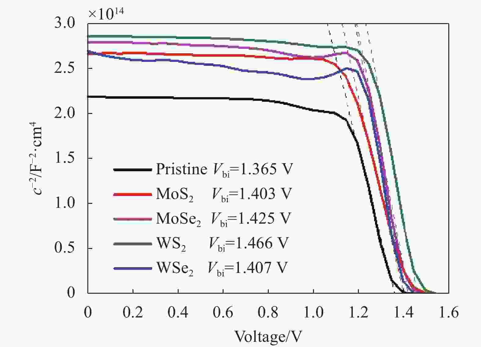
      Figure 9.  Mott-Schottky curves of the PSCs with and without TMDCs modification

      式中:c为器件电容;Vbi为器件的内建电势;V为施加的电压;A为有效电池面积;e为元电荷;ɛ为钙钛矿的相对介电常数;NA为界面的电荷密度。原始器件的Vbi为1.365 V,TMDCs修饰后器件的Vbi分别提升到1.403 V (MoS2)、1.452 V (MoSe2)、1.466 V (WS2)和1.407 V (WSe2),这表明TMDCs修饰后器件中电荷分离的驱动力增强,耗尽区扩大,因此抑制了电荷复合[20]。Mott-Schottky曲线中较大的斜率(图9中的虚线)也表明TMDCs修饰后器件的界面电荷密度较低[21]。这主要是由于TMDCs修饰提升了钙钛矿晶体的质量,减少了界面缺陷,而这些缺陷会成为复合中心阻碍载流子转移和提取。

      器件优化后性能提升主要是得益于高质量的钙钛矿薄膜和界面能级匹配改善了载流子的传输并抑制了非辐射复合。器件的电子提取能力与其瞬态荧光寿命密切相关。图10(a)是钙钛矿薄膜在不同TMDCs修饰后的TRPL衰减曲线。衰减曲线可以使用如下双指数函数拟合[22]

      Figure 10.  (a) TRPL decay curves and (b) PL curves of perovskite films with and without TMDCs modification

      式中:I为样品被激发的荧光光强;τ1为非辐射复合缺陷相关部分;τ2为辐射复合缺陷的相关部分。根据τave=(a1τ12+a2τ22)/(a1τ1+a2τ2)计算平均衰减时间τave,以评估器件的电子提取能力,其中a1a2分别代表τ1τ2的比例[23]

      表2列出了拟合得出的τ1τ2τave等相应参数。从表中可以看出,不同TMDCs修饰后的CsPbBr3钙钛矿薄膜的τave均有不同程度的降低,原始薄膜的τave为0.788 ns,TMDCs修饰后分别降低到0.738 ns (MoS2)、0.713 ns (MoSe2)、0.653 ns (WS2)和0.720 ns (WSe2)。由于TMDCs修饰后器件中ETL/钙钛矿界面用于电子提取的导带具有更好的能级匹配,同时界面缺陷更少,因此电荷提取更快,使CsPbBr3在不同的TMDCs修饰层上均表现出较短的载流子寿命。此外,钙钛矿薄膜的PL峰强度也高度依赖于电子-空穴的辐射复合。在将TMDCs引入界面时,钙钛矿薄膜的PL峰强度显著降低(图10(b)),这表明电子从钙钛矿到SnO2 ETL的提取能力增强,因此钙钛矿导带上光生电子的寿命无疑会缩短,这也与前面的TRPL测试结果一致。

      Sampleτ1/nsa1τ2/nsa2τave/ns
      Pristine0.53866.08%8.34933.92%0.788
      MoS20.57275.69%7.78324.31%0.738
      MoSe20.46864.09%10.73235.91%0.713
      WS20.53780.64%6.42819.36%0.653
      WSe20.57978.68%6.87521.32%0.720

      Table 2.  TRPL fitting parameters of perovskite films with and without TMDCs modification

    • 文中针对制约全无机CsPbBr3 PSC效率提升的界面能级匹配和钙钛矿晶体质量导致的载流子复合等问题,利用不同的二维TMDCs材料作为界面修饰层促进界面电荷提取以提高全无机CsPbBr3 PSC的性能。通过在ETL与CsPbBr3界面之间引入二维TMDCs层状材料,构建TMDCs/CsPbBr3范德华异质结,利用晶格匹配的范德华外延生长以及TMDCs的二维层状结构特点,生长高质量的CsPbBr3钙钛矿薄膜,同时减小界面能级势垒,降低钙钛矿层与ETL之间的界面电荷损失,将碳基全无机CsPbBr3 PSC器件的效率从7.94%提升到10.02%,同时开路电压从1.474 V提升至1.567 V。文中为制备高质量的钙钛矿薄膜同时实现界面能级匹配开辟了一条新途径,其不仅可用于制备高性能PSC,而且还可用于其他基于钙钛矿薄膜的光电器件。

Reference (23)

Catalog

    /

    DownLoad:  Full-Size Img  PowerPoint
    Return
    Return