


-
随着精密加工技术的进步,纳米技术的研究取得了巨大的成就,被应用于光电子器件等多个领域[1-2]。微型化光学系统在光通信、光存储、半导体器件等领域发挥了巨大的作用,微纳结构的光学特性渐渐成为了近年来的热门研究方向[3-4],具有表面微结构的光学元件的应用日趋广泛[5-6]。微透镜阵列作为基本光学元件之一,不仅可以实现与传统光学元件相同的聚焦和成像等功能,还由于其体积小、集成度高和可阵列化等优点,被广泛应用于光刻机、光场相机、太阳能电池系统和3D显示器等多种光学器件与仪器中[7]。为了获得具有不同光学性质和几何形状的微透镜阵列,已经开发出多种成熟的工艺技术。其中,热回流技术可以通过将预先准备的聚合物圆柱体制备成半球形,从而快速获得微透镜阵列,这种制备方法可以通过合理调节聚合物圆柱体之间的距离获得具有较高的填充因子[8]的微透镜阵列。激光直写技术可以精确制备具有复杂三维轮廓的微透镜阵列[9-10],然而其生产效率较低。随着光学元件小型化的发展趋势,光刻技术目前在微加工领域具有广泛的热度。这种技术可以将掩模版上的图形转移到涂有光刻胶的硅片上,通过一系列的操作绘制出硅片表面薄膜上具有微透镜阵列的三维模型,是一种可以制备精密、细微和复杂薄膜图形的化学加工方法。
近年来,利用微流体操控技术制备微透镜阵列以其灵活的可调控性、制造工艺简便性、制造成本低廉性以及材料选择性广泛等优点在微透镜制造领域激发了广泛的研究热度[11],这种技术的基本原理是使微流体克服粘性阻力从而使液面发生弯曲来制备微透镜阵列。由于微孔内微流体、微孔内空气和微孔壁之间的表面张力作用,微孔内的微流体表面会发生弯曲。微透镜的表面曲率可以通过调节衬底与微孔阵列之间的间隙来控制。在之前的研究中,已经实现了通过在微孔上旋涂聚合物树脂快速制作微透镜[12-13]。然而,对于大多数用于制造微透镜阵列的微流体操控技术,由于在制造过程中需要利用微孔制备微透镜,微孔之间的间隔占据了有效的空间,使得制备的微透镜阵列的填充率较低。
文中提出了一种全新的高填充因子微透镜阵列的制备技术,这种技术基于微流体操控技术的原理,且具有快速、简易的优点。通过这种方法制备的微透镜阵列可以生成在微柱阵列上,且制备出微透镜可以被紧密地封装在一起。
-
微透镜阵列的制备过程如图1所示。通过光刻技术在硅片上制备出具有预先结构设计的微孔阵列模型,将主剂与固化剂的质量比按照10∶1的比例混合制备聚二甲基硅氧烷(PDMS),将其浇注进具有微孔结构的硅板上。设置烘箱温度为60 ℃烘烤6 h固化,待固化完成后取出硅片静置并冷却至室温,制备出一组具有和微孔结构形状互补的微柱阵列结构作为基底。将固化的PDMS基板表面和玻璃板表面做等离子处理2 min后,使PDMS基底与玻璃板相互贴合并充分接触,设置烘箱温度为60 ℃烘烤6 min完成键合。
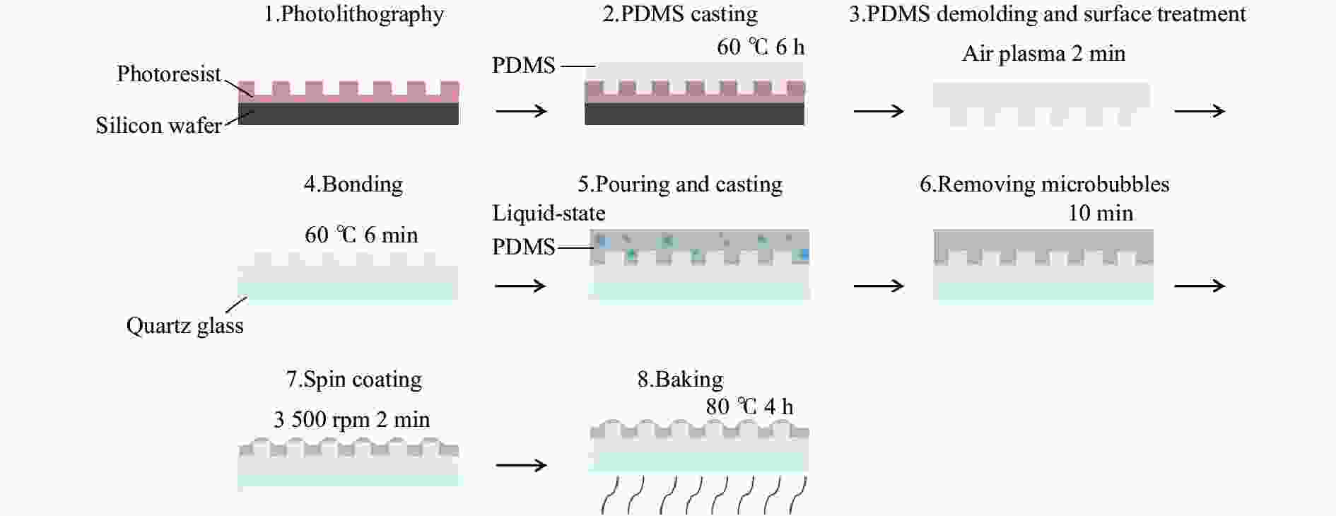
Figure 1. Fabrication of the microlens array on the micro-posts
同时,配制另一部分预聚物质量比例为10∶1的PDMS液体,倾倒在键合好的基底上。将样品置于真空机中真空处理10 min,去除液体PDMS中的微气泡,使液体PDMS进入到PDMS微柱的间隙中。将样品置于离心机中,设置转速为3 500 rpm旋转2 min进行旋涂。经离心机旋涂处理后,部分PDMS将残留在基体上,表面呈波浪形。由于衬底表面的微柱存在,位于微柱顶端的PDMS呈球帽状,微柱之间的PDMS呈逐渐向下弯曲的形状,这种现象是毛细管效应导致的。而微柱之间的PDMS连续连接,表面呈谷状。因此,PDMS在衬底上的轮廓呈波浪形。最后,设置烘箱温度为80 ℃,将PDMS烘烤固化4 h完成制备。
尽管大部分PDMS都会均匀分布在微柱四周,仍有部分PDMS留存在微柱顶部。由于表面张力的作用,微柱上的PDMS呈球帽状,而微柱周围的PDMS会附着在柱上并逐渐向下弯曲,这一现象可以用壁效应来解释。
-
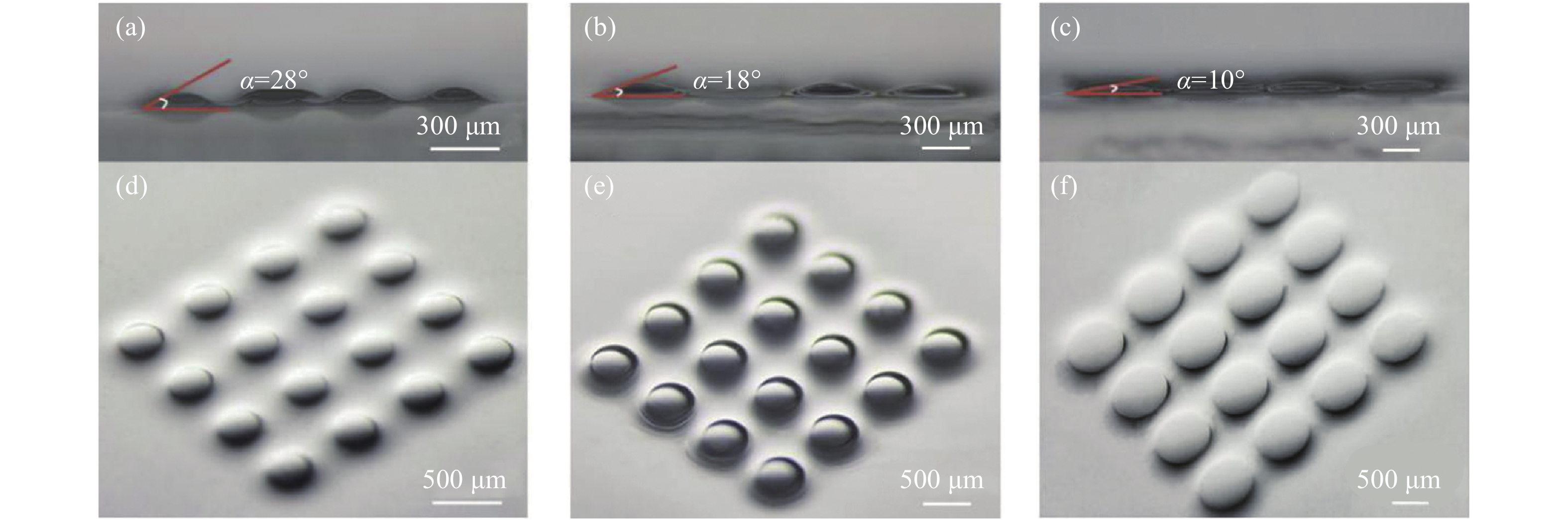
通过该制备工艺制备的三种不同尺寸的4×4微透镜阵列如图2所示。从图2(a)~(c)中可以看出,微透镜阵列的接触角随着微透镜直径的增加而减小。这是由于在转速和旋涂时间相同的情况下,微柱阵列的直径越大,残留在微柱上的PDMS越薄,形成的微透镜阵列即越平滑。图2(d)~(f)分别为微柱直径为300、500、700 μm的微透镜阵列,微透镜阵列中的每个微透镜都具有相同的形状特征且彼此相连。从水平方向观测并计算得到这三种微透镜的曲率半径依次为319、809、2 016 μm。微透镜的焦距f计算公式如下:
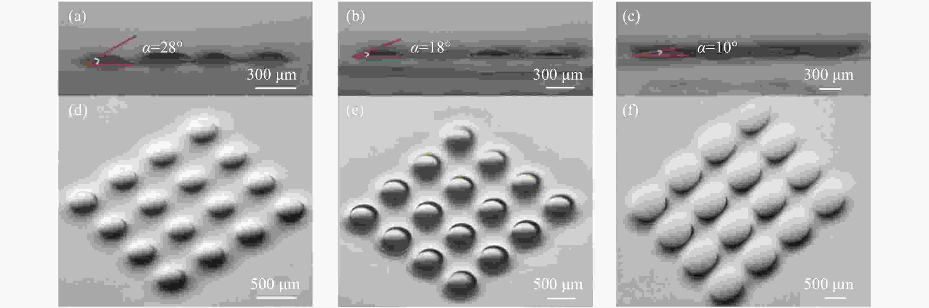
Figure 2. Microlens arrays through a microscope. (a)-(c) Side view of the 4×4 microlens arrays in three size (300,500 and 700 μm) of the arrays of micro-posts; (d)-(f) Top view of the 4×4 microlens arrays in three size (300,500 and 700 μm) of the arrays of micro-posts
式中:d为球形顶部的直径;h为球形顶部的高度;n为PDMS的折射率,即n=1.403。通过计算得出微透镜的焦距依次为0.8、2、5 mm。
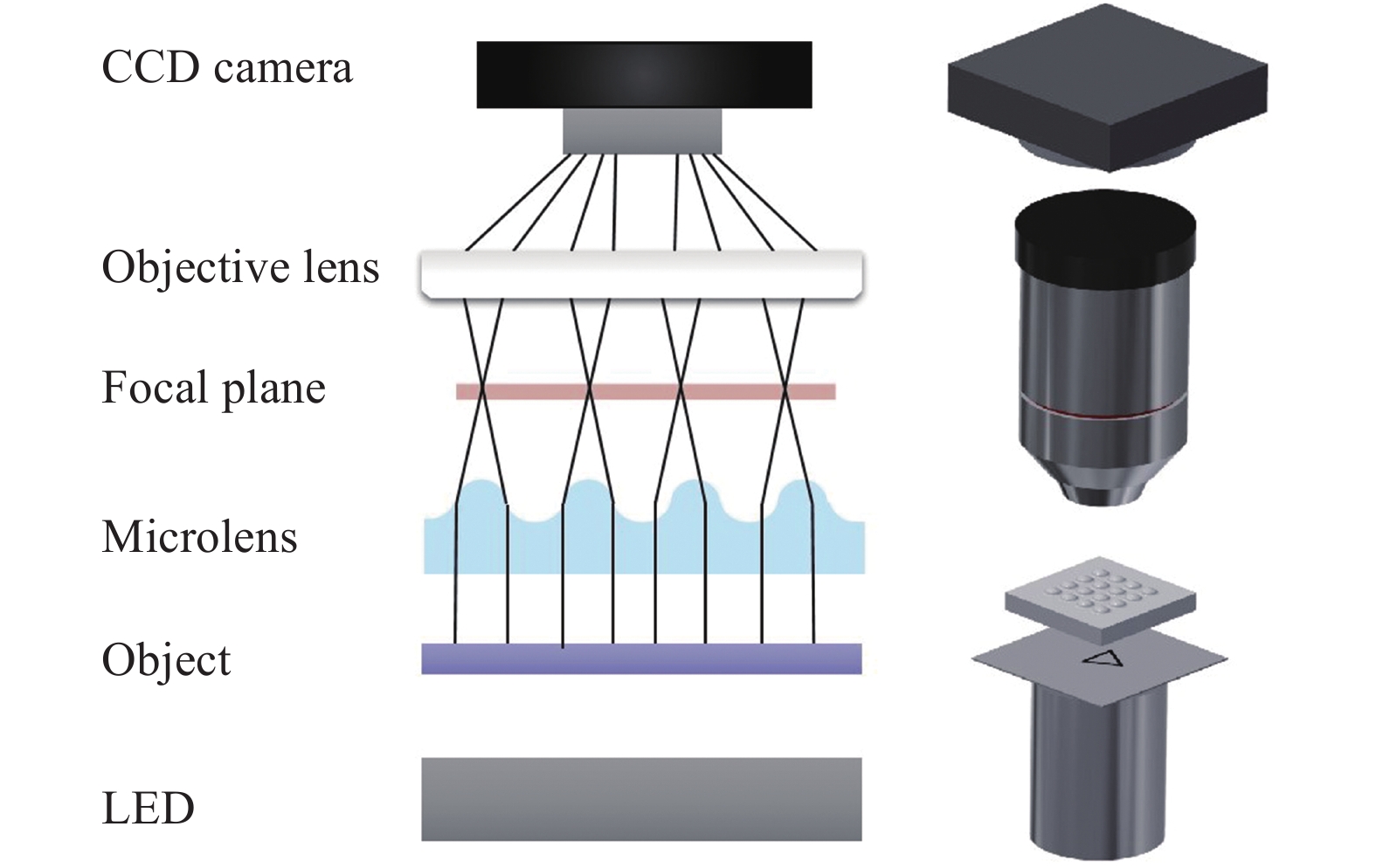
为了评估微透镜阵列的成像性能,搭建了如图3所示的成像系统。用白光LED照射物体,微透镜阵列置于物体后方以捕捉图像,实验中采用了USAF 1951标准的分辨率精度板作为观测目标对象。微透镜阵列的焦平面与物镜的焦平面对齐,使物镜从微透镜上获取清晰准确的图像。最后,利用电荷耦合器件(CCD)摄像机记录图像。
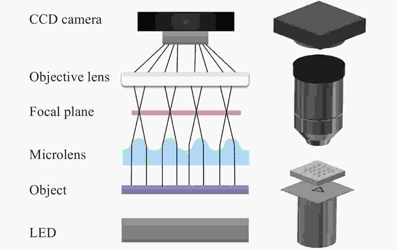
Figure 3. Imaging system of microlens arrays
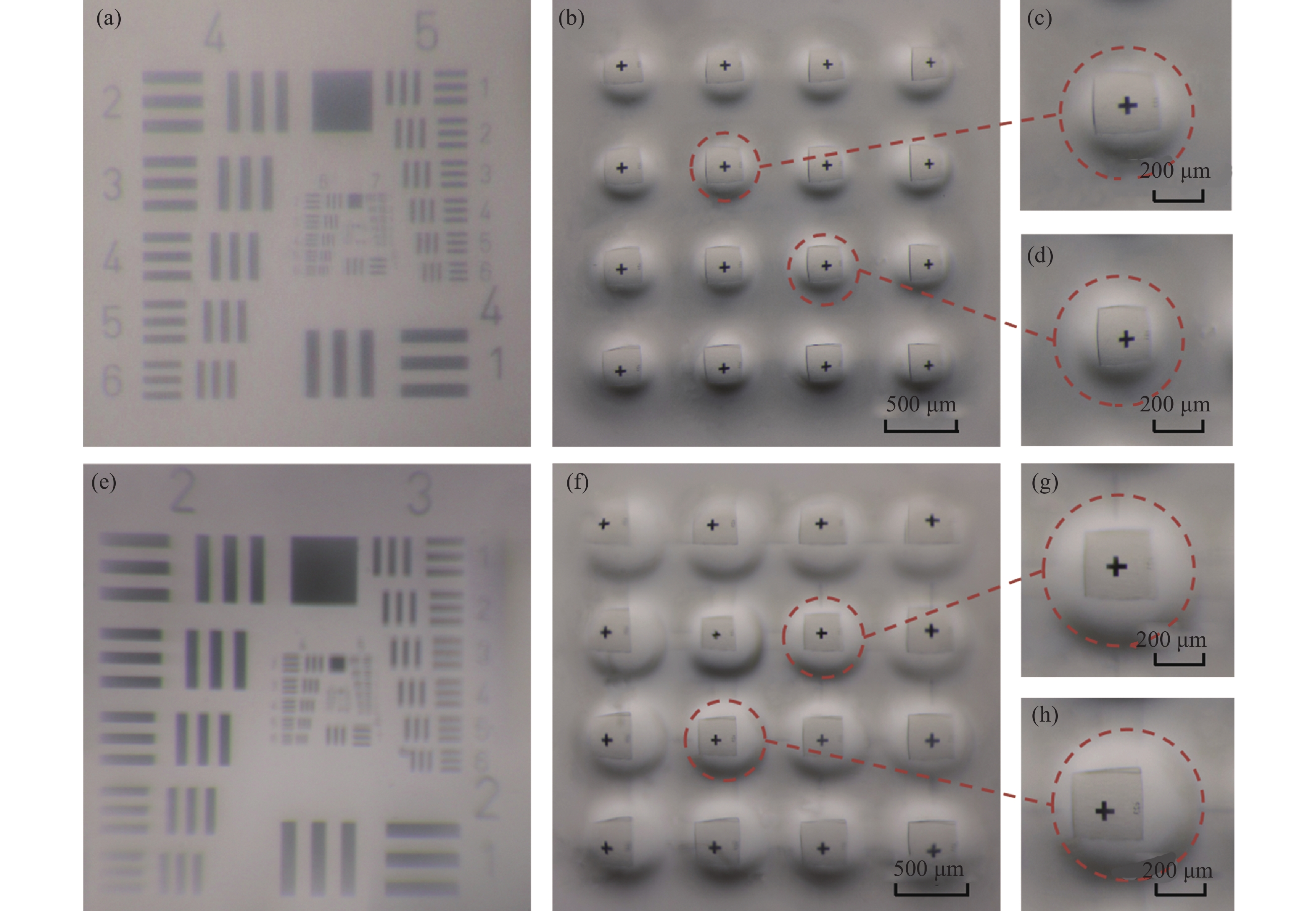
图4为通过尺寸300 μm和500 μm微柱上形成的微透镜阵列成像所获得的照片。从图4(a)中可以看出在USAF 1951年分辨率精度板上,通过微透镜阵列成像后的照片可以观察到第6组第1号元素的线对,由此得出尺寸为300 μm微柱上形成的微透镜阵列的分辨率可以达到8 μm。同样,从图4(e)中可以看出在USAF 1951年分辨率精度板上,通过微透镜阵列成像后的照片可以观察到到第4组第2号元素的线对,由此得出尺寸为500 μm微柱上形成的微透镜阵列的分辨率可以达到28 μm。
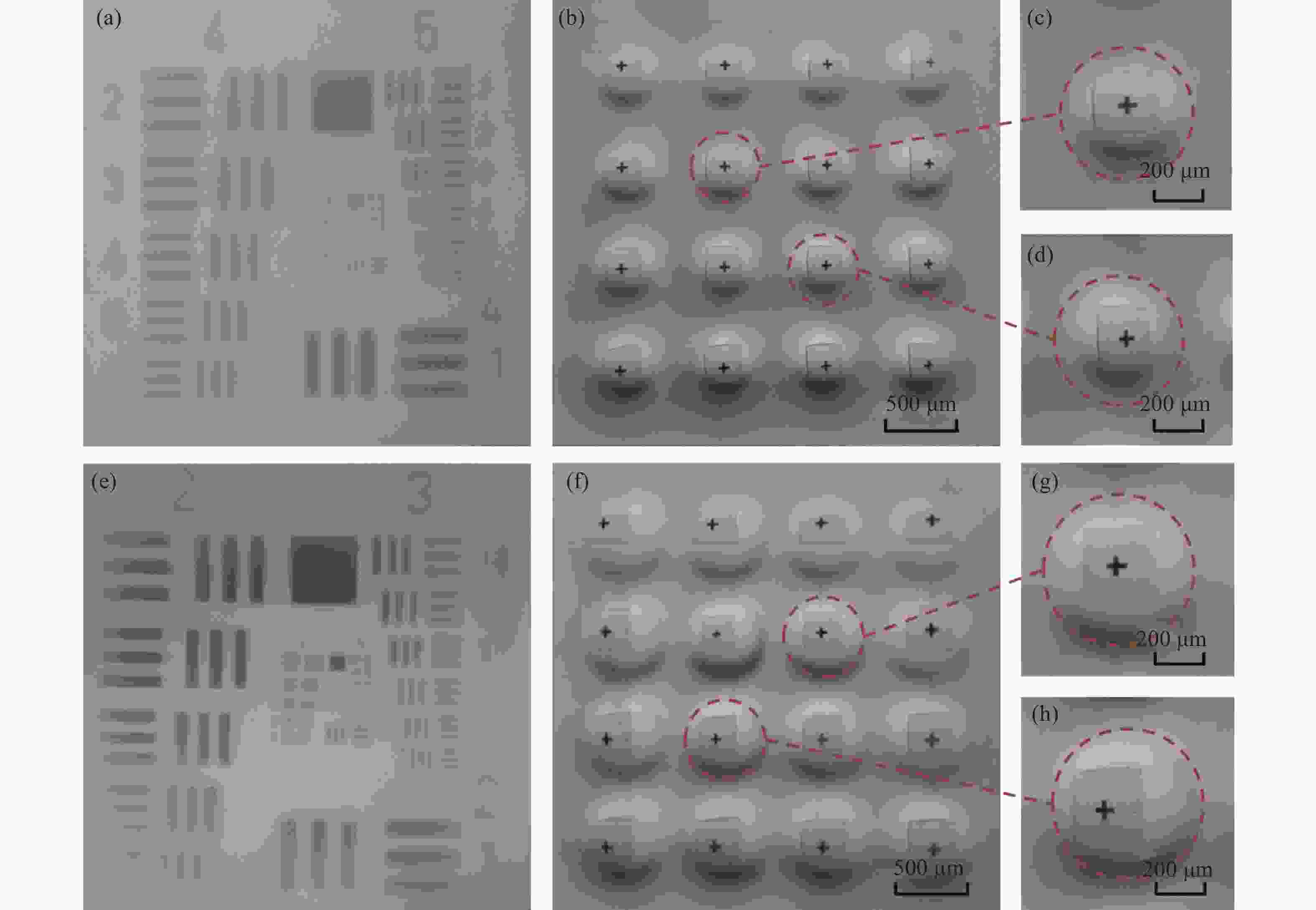
Figure 4. Images observed by using the 4×4 microlens array in 300 μm and 500 μm of the array of micro-posts. (a) Microscopic image of USAF 1951 resolution target obtained from a single microlens; (b)-(d) Images of the cross-shaped pattern obtained from the microlens array
此外,还测试了一组十字图案通过微透镜阵列成像的效果图,从图中可以看出一组十字形图案可以被明显观测到。其中通过尺寸为300 μm微柱上形成的微透镜阵列成像的十字图案自定义的线宽为240 μm,通过微透镜阵列成像的图片如图4(b)所示。通过尺寸为500 μm微柱上形成的微透镜阵列成像的十字图案自定义的线宽为280 μm,通过微透镜阵列成像的图片如图4(f)所示。由于待成像图案与微透镜阵列相对位置的限制,无法获取通过尺寸为700 μm微柱上形成的微透镜阵列的十字成像,但依然可以得出结论,通过这种工艺制备出的具有高填充因子的微透镜阵列满足不同待观测物体的观测要求。
分别任意取两组微透镜阵列中的两个微透镜所成的十字物像,如图4(c)、(d)、(g)、(h)所示。从图中可以分别看出两组微透镜阵列中的十字像均在每个微透镜中的位置略有不同,这是由于十字图案与微透镜的相对位置不相同。尽管如此,无论是从尺寸为300 μm微柱上形成的微透镜阵列观察到的十字图案还是从尺寸为500 μm微柱上形成的微透镜阵列观察到的十字图案在形状上具有高度的均一性,没有明显的失真现象。成像结果表明,实验中制备的微透镜阵列具有良好的成像性能,且可以通过调节制备过程中微透镜阵列的尺寸实现不同精度要求的物像观测。
-
文中提出了一种新型的微透镜阵列制备工艺,由预先制备的聚合物微柱阵列来实现微透镜阵列的制备。通过制备过程的光刻阶段中调节微柱的尺寸和微柱与微柱的间隔(微柱直径分别为300、500、700 μm),可以制备出不同直径、曲率半径和接触角等特性的微透镜阵列。通过实验得出结论,微透镜阵列的接触角随着微柱直径的减小而增加,微柱直径为300 μm的微透镜阵列分辨率最高。且这种方法制备的微透镜阵列具有高填充因子的性质和分布均匀的特点,由于模具中不含有间隔微透镜单元的结构,每个微透镜可以自然地在微柱阵列上成形,微透镜相互之间紧密相连,因此可以获得具有高填充因子的微透镜阵列。在微透镜阵列的光学成像性能方面,不同特性的微透镜阵列均表现出了良好的成像质量。文中主要研究了通过调控微孔模具的尺寸来操控微透镜阵列的制备,关于未来的研究方向,还可以研究温度对制备微透镜阵列的影响。在微孔模具尺寸与间隔不变的情况下,通过改变微孔间的温度操控微透镜阵列的曲率,从而实现微透镜阵列焦距的调控。此外,目前的微流控操纵技术制备的透镜大多为球面透镜,在未来的研究中,可以尝试制备非球面透镜,甚至自由曲面的透镜。通过这种方法制备的微透镜阵列,不仅可应用于制备更大面积的透镜阵列,还具有广泛的应用前景。例如,可以将这种微透镜阵列的制备工艺应用于蝇眼透镜,制备曲率可调控的蝇眼透镜,实现不同焦面的待观测物体的图像的捕获。
Rapid fabrication and characteristics analysis of high-filling-factor microlens array
doi: 10.3788/IRLA20200476
- Received Date: 2020-12-20
- Rev Recd Date: 2021-04-10
- Publish Date: 2021-10-20
-
Key words:
- microlens array /
- micro-fabrication /
- microfluid-manipulation techniques /
- high-filling-factor
Abstract: As a precise optical component, microlens array has applications in fields as optical information processing, optical sensing, optical computing, optical communications and high sensitivity imaging. Researchers have developed many advanced fabrication techniques, some of which already realized the preparation of the microlens array with required geometries, profile and optical properties. However, it would be extremely difficult to achieve a compact packing as such 3D micro-manufacturing techniques are hard to control. A novel rapid and low-cost microfluidic-manipulation based technique was proposed to fabricate high-filling-factor microlens array. A brief demonstration of the fabrication was given, which had excellence of suited to volume production and significant productivity boost. Meanwhile, the microlens arrays of three different properties were produced, which were realized by adjusting the size of the array of micro-posts whose sizes were 300, 500, 700 μm in diameter, respectively. The imaging system was set up to demonstrate the imaging performance of each of the microlens array, evaluating the precision of each microlens array and imaging uniformity of the microlens array. The results show that the fabricated microlens arrays have good imaging performance and have a promising prospect in the use of 3D imaging and optical uniformity.

 DownLoad: