


-
色散,作为基本的物理现象广泛存在于各种光学介质当中,其在很多领域都有着广泛的应用。在高速光纤通信中,色散被用来抑制非线性,同时可以用不同符号的色散进行相互补偿,扩展传输距离[1]。在微波光子学中,由于光纤色散引入的频率选择性衰落效应是实现微波光子滤波器的基本原理[2]。另外,在微波相控阵天线阵列中,利用光载微波信号实现真时延能有效地对抗宽带波束展宽效应,可以大大扩展微波相控阵天线的工作带宽[3-4]。在光纤系统中,目前常用的色散介质主要是光纤。虽然光纤具有低损耗大带宽的特性,但是由于单位长度色散值很低,通常需要很长的光纤来实现大色散,这样就增加了系统尺寸、非线性和不稳定性[5]。为解决这个难题,啁啾布拉格光纤光栅的概念被提出,利用光纤光栅的连续频率反射特性获得色散和延迟效应,具有小体积、低非线性的特点,在大规模微波光子相控阵天线中作为真延时器件而广泛使用[6-7]。但是,啁啾光纤光栅的工作带宽通常较小(<1 nm),而且容易受到外界干扰。近年来,随着集成光子学的蓬勃发展,集成平台上的波导布拉格光栅也随之成为研究的热点 [8]。相比起传统的使用紫外曝光制作的光纤布拉格光栅,集成平台上的啁啾布拉格光栅具有稳定性更好,集成度更高的优点。而在集成布拉格光栅中,集成环绕型啁啾布拉格光栅在加工稳定性和器件尺寸上都显示出了得天独厚的优势 [9],它在芯片上的排布不再是一根直线,而是被卷曲为圆环状排布。这种排布可以使整个器件的结构更加紧凑。在啁啾布拉格光栅的大多数应用中,都需要其具有较大的群延迟,因此这需要啁啾布拉格光栅的长度尽量的长。然而,到目前为止,片上集成啁啾布拉格光栅的长度仍然被局限在毫米量级,其群延迟大小最大也只在百ps量级。文中提出了一种新型的低损耗波导光栅制作方法,有效地增长了光栅长度,并实现了最大2440 ps的群时延,带宽达到9.4 nm。
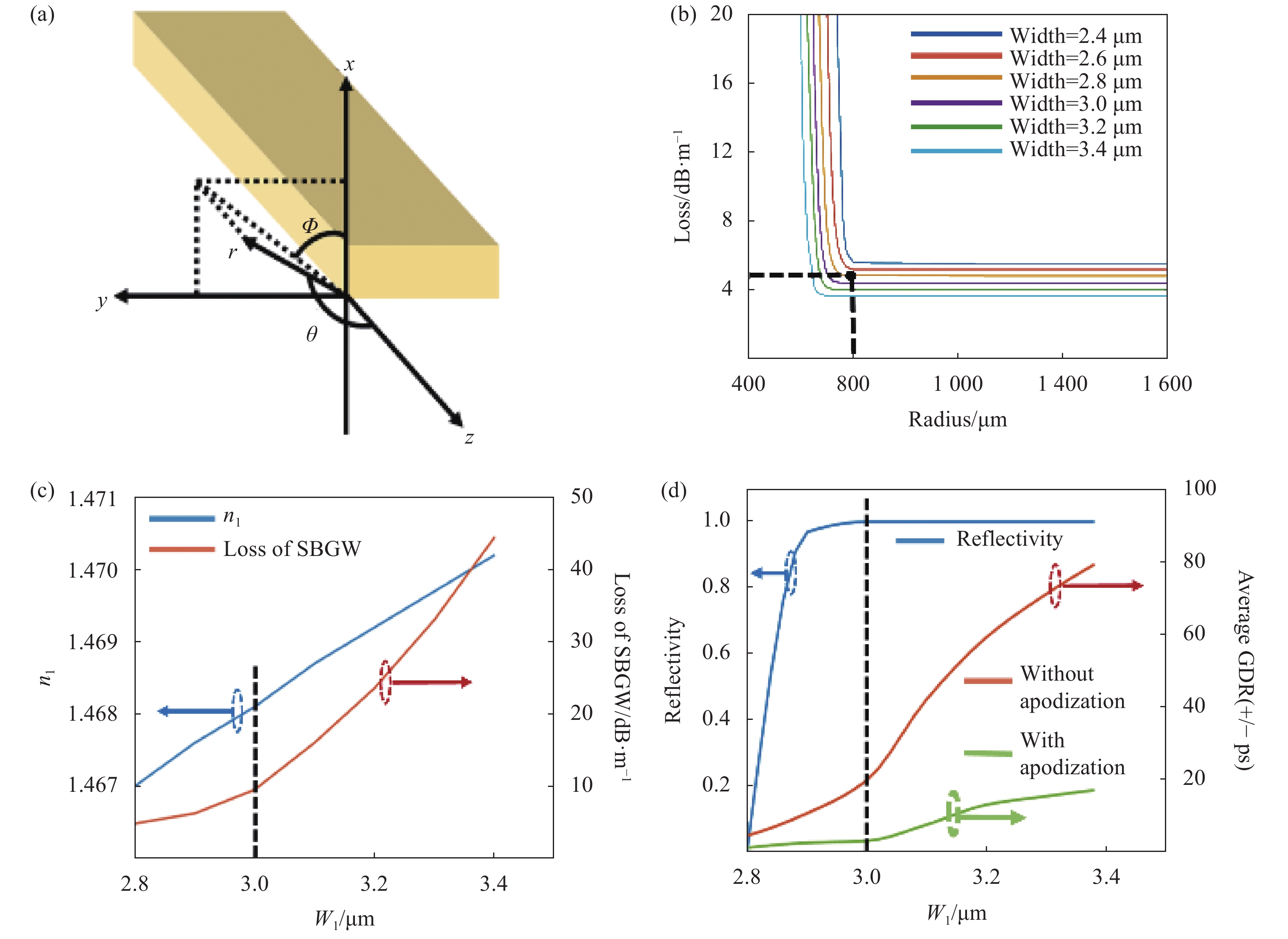
集成啁啾布拉格光栅的长度主要受限于光波导的损耗,而这其中由界面粗糙度带来的界面散射损耗和弯曲波导模式泄露带来的弯曲损耗是最重要的因素。笔者所在团队使用三维体积电流法[10]在特定粗糙度的情况下对集成平台上矩形波导的界面散射损耗做了分析,同时利用有效折射率法[11]将弯曲波导等效成直波导,从而得到了在厚度为90 nm的氮化硅平台上矩形波导的损耗随宽度和弯曲半径的变化关系,结果如图1(b)所示。可以看出波导的损耗是随着波导宽高比以及弯曲半径的增大而降低的。为了维持波导中单模传输的条件文中将波导的宽度设置为2.8 μm,最小弯曲半径设置为800 μm。

Figure 1. Loss analysis of waveguide and the influence of Δneff on grating performance. (a) Loss analysis coordinate system; (b) Loss changes with aspect ratio and bending radius of the waveguide; (c) Grating overall loss and neff1 change with w1; (d) Grating reflectivity and GDR change with w1
除了波导的损耗之外,另一个对布拉格光栅的性能具有较大影响的参数是其折射率调制深度。设啁啾布拉格光栅中心波导的宽度为w0,有效折射率为neff0,法向波导的宽度为w1,有效折射率为neff1。那么折射率调制深度可以被表示为
$ \Delta ne\!f\!\!f= (ne\!f\!\!{f}_{1}- $ $ ne\!f\!\!{f}_{0})/2 $ 。图1(c)和图1(d)显示了布拉格光栅的各项性能随Δneff的变化。可以看到,当w1增大时也即折射率调制深度增大时,啁啾布拉格光栅的损耗和群延迟振荡幅度会增加,所以折射率调制深度不宜过大。但在折射率调制深度太小的情况下,布拉格光栅的反射率可能会不足100%,这会带来额外的功率损失。因此折射率调制深度的最佳取值是啁啾布拉格光栅反射率刚好达到100%时的值,此时Δneff =5e-4。通过对波导损耗的分析确定了波导最优的宽高比以及弯曲半径,通过对折射率调制深度的分析,确定了其sidewall(城墙)型边缘的凸起程度。利用氮化硅加工平台和螺旋形光栅结构,实现了硅基集成的大色散啁啾布拉格光栅芯片,如图2所示,光栅最长达到了23.4 cm。而后对其进行加工测试,测试结果如图3(a)所示。由图3(a)可以看到啁啾布拉格光栅的带宽达到了约9.4 nm,色散值达到了259.57 ps/nm,群延迟达到了2.44 ns,群延迟振荡幅度(GDR)约为
$ \pm {\rm{32}}\;{\rm{ps}}$ 。
Figure 2. Silicon integrated chirp Bragg grating chip. (a) Micrograph; (b) SEM of waveguide; (c) SEM of spiral grating
虽然测试中得到的GDR的值相对于其整体群延迟大小来说已经比较优秀了,但是对绝大多数应用来说 GDR的值越小越好。降低GDR主要是采用在啁啾布拉格光栅的频域周期性的加矩形窗切趾来实现,最终实现了GDR成功降低至约
$ \pm {\rm{24}}\;{\rm{ps}}$ ,如图2(b)所示。另外,在实际加工过程中,加工误差会沿着光传播的方向不断累积,越靠近光栅末端则群延迟振荡会越大。这主要是因为光沿着光栅传播的越深入,那么它穿过的均匀布拉格光栅的个数就越多,在加工误差存在的情况下,被光栅不同位置误反射的概率就越大。如图2(c)所示,这是一个长度为13.8 cm的啁啾布拉格光栅的反射谱和群延迟曲线,除了长度之外,它的其他参数与前文中介绍的长度为23.4 cm的光栅基本相同,但是GDR却只有$ \pm {\rm{27}}\;{\rm{ps}}$ ,经过切趾之后其GDR甚至可以降低到大约$ \pm {\rm{8}}\;{\rm{ps}}$ 的水平,如图2(d)所示。因此,对于啁啾布拉格光栅来说,除了损耗之外,加工误差引起的性能恶化也是在设计其长度时必须要考虑的因素。综上所述,文中通过对集成平台上波导形状的合理设计以及折射率调制深度的深入分析实现了带宽9.4 nm,群延迟2.44 ns的啁啾布拉格光栅,这是目前报道过的片上啁啾布拉格光栅中所能实现的最大的群延迟。如表1所示,与其他集成光延时方案相比,文中提出的芯片在最大延时量、延时带宽积、单位面积延时带宽积等方面具有明显优势,在微波光子学、高速光纤通信系统及光信号处理领域有着非常广阔的应用前景。
Ref. Group Group delay
/psTunability
/psBandwidth
/nmSize
/mm2Delay bandwidth
product/ps·nmDelay bandwidth product
per unit area
/ps·nm·mm−2Material Technology [12] K.J.Vahala 68000 N/A Wideband 9025 - - Silicon Path select [13] S.S.Patel 2560 Tunable 0.2 1200 512 0.43 SiO2 [14] D.J.Blumenthal 12350 850 >40 3825 >494000 129.15 Silicon Nitride [15] T.Baba 54 Tunable 3 16.48 162 9.83 Silicon Slow light [16] R.T.Chen 216.7 Tunable 25 0.18 5417.5 30097 Silicon [17] D.V.Plant 96 Tunable 8 0.015 768 61200 Silicon Bragg grating [18] K.petermann 450 Tunable 1.2 >100 540 <0.54 Silicon [19] J P.Chen 110 10 0.08 ~1 8.8 ~8.8 Silicon Micro-ring [20] Andrea Melloni 800 100 0.08 ~1 64 ~64 Silicon Oxynitride - H.W.Chen(this work) 2440 N/A 9.4 9.07 22936 2528 Silicon Nitride Bragg grating Table 1. Performance comparison of different schemes to realize group delay

Figure 3. Chirped Bragg grating response and the apodized chirped Bragg grating response obtained in the experiment. (a) Chirped Bragg grating response with length of 23.4 cm; (b) Apodized chirped Bragg grating response with length of 23.4 cm; (c) Chirped Bragg grating response with length of 13.8 cm; (d) Apodized chirped Bragg grating response with length of 13.8 cm
Wideband large dispersion group delay chip based on silicon photonics integration (Invited)
doi: 10.3788/IRLA20211045
- Received Date: 2021-04-06
- Rev Recd Date: 2021-05-22
- Publish Date: 2021-07-25
-
Key words:
- integrated photonics /
- chirped Bragg grating /
- dispersion compensation
Abstract:
Content integrated, broadband, large group delay devices have important applications in microwave photonic filtering, true delay phased array antenna and other fields, which can effectively reduce the system size and power consumption. In this paper, a broadband large dispersion delay chip based on silicon-based photonic integration was proposed and implemented. By using ultra-low loss waveguide structure and side wall normal vector modulation structure, on-chip integration of large dispersion waveguide grating was realized. The dispersion was about 250 ps/nm, maximum group delay was 2440 ps and the bandwidth was more than 9.4 nm. The chip is expected to be used in microwave photonics, high-speed fiber communication system and other fields.


 DownLoad: