


 下载:
下载:


-
超快激光是指利用锁模技术产生的脉冲宽度极窄的超短脉冲激光,其脉冲宽度通常定义为皮秒(10−12 s)~飞秒(10−15 s)量级。早在20世纪60年代,研究者们就开始利用激光锁模技术来开发超快激光加工技术;1985年,由Strickland和Mourou等人发明的啁啾脉冲放大技术是超快激光的一项革命性进展,推动了其基础研究[1];1991年,Spence等人报道了一种脉冲宽度低于100 fs的自锁模的掺钛蓝宝石激光器[2],大大提升了超快激光运转的稳定性,推进了超快激光向飞秒激光领域发展;20世纪光纤啁啾脉冲放大器的研制和基于半导体泵浦的掺稀土激光介质的高功率超快激光系统的开发改善了超快激光系统的性能,为实现更可靠的超快激光加工作出了重大贡献。目前,超快激光器已被广泛应用于基础研究和实际应用。
作为一种加工技术,飞秒激光已被证明是在微纳米尺度上进行先进材料加工的有力工具。飞秒激光加工技术依赖于飞秒激光器和飞秒激光加工系统的发展。飞秒激光器主要分为染料激光器、固体激光器、光纤激光器和半导体激光器。目前,国内外各研究机构均开发出了一些高精度、高稳定性和易于操控的加工系统。例如,德国的 Kugler、美国的Oxford Lasers、日本的Cyber Laser、国内的大族激光等。未来,高功率激光器和易用的加工系统将使得飞秒激光加工从特种制造技术变成一个通用的微纳制造工具。
飞秒激光具有很多独特属性,如超短脉冲持续时间、极高的峰值强度、宽频率范围等,这些独特属性从根本上改变了激光与物质相互作用的方式,展现出了其在微纳制造领域中的独特优势和广泛的潜在应用。(1)在时间尺度上,飞秒激光的超短脉冲宽度限制了热影响区的形成,这对超高精度制造至关重要;(2)在空间尺度上,飞秒激光与材料作用体现出多种非线性过程,例如,非线性的光学吸收、非线性的化学反应和非线性的材料改性等,借助这些非线性过程可以打破光学衍射极限,实现纳米尺度微结构制备;(3)在材料的维度上,极高的峰值强度允许激光与几乎任何物质发生非线性相互作用,这种材料的广谱适用性丰富了可加工材料的种类,能够实现软、硬、脆等多种难加工材料的微结构制造。目前,飞秒激光已经能够实现对金属、氧化物、陶瓷、软材料(聚合物和生物组织)、硬脆材料(金刚石、蓝宝石等)等多类功能材料的精细加工[3-4]。
近年来,可加工材料种类的丰富和加工精度的提升也拓展了飞秒激光加工技术的应用领域,如在微光电、微机械、微传感、仿生微结构、微流控、微纳机器人等前沿领域的应用拓展[5-8]。飞秒激光具有真三维的微纳结构成型的能力,可通过编程设计实现各种精细微图案和微结构制造,可以在材料内部制备微纳结构,可以灵活地实现材料去除、材料改性以及材料沉积,能够满足各类微结构制造及微部件集成的技术需求。如今,飞秒激光加工技术已成为各类难加工材料、复杂微结构和超精密微器件制备的前沿核心技术。
文中综述了以飞秒激光为代表的非线性激光微纳制造的研究进展与应用,讨论了飞秒激光加工的技术特点和加工方式,详细介绍了飞秒激光加工在微纳光学、微流体器件、多功能结构化表面和生物医学工程领域的创新应用。最后,展望了飞秒激光加工技术的未来发展前景和挑战,探讨了飞秒激光制造工艺未来的研究方向。
-
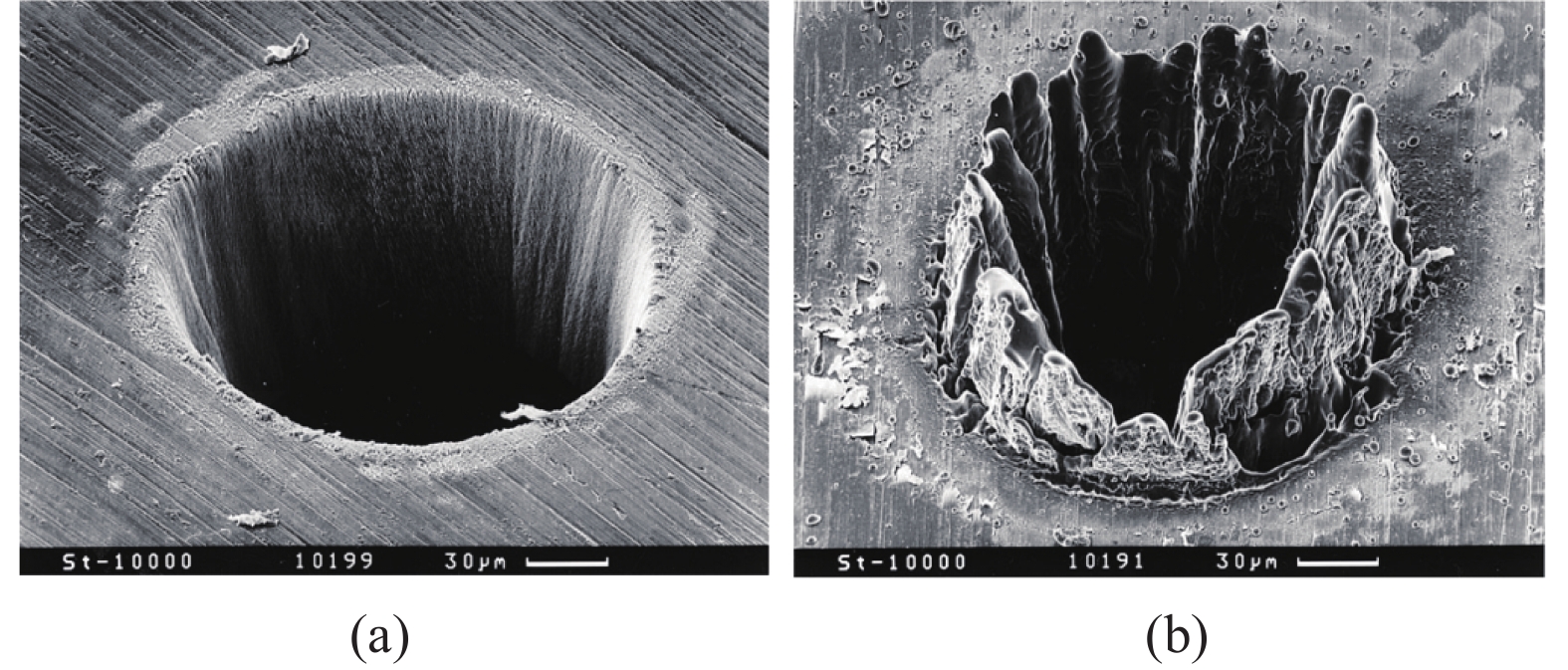
与纳秒或者更长脉冲的激光加工过程相比,飞秒激光加工通常被称为非热加工过程。这使飞秒激光在材料加工中展现出了更加优异的性能,能够实现高精度、高质量的微纳制造。对于长脉冲激光(例如大于1 ns),材料被加热后有足够的时间在聚焦体积内熔化,并扩散到周围材料中。熔融材料的一部分蒸发并以高速微滴的形式喷射,其余熔融材料重新凝固,这导致材料的加工质量较差,形成热影响区、浮渣和微裂纹等缺陷。相比之下,对于飞秒激光来说,由于其脉冲时间极短,热扩散的长度通常比激光穿透长度小得多。因此,飞秒激光可以诱导材料快速电离,并将辐照体积区域的材料直接转化为等离子体、蒸汽和纳米液滴的混合物,随后进行喷射。而在加工过程中产生的材料融化和热扩散可忽略不计,从而可以实现高清洁度和高精密的加工质量[9]。图1表明了长脉冲激光和飞秒激光加工之间的明显差异[10]。图1(a)和1(b)为利用飞秒激光(200 fs)和纳秒激光(3.3 ns)在100 μm厚的钢箔上钻孔的扫描电子显微镜(SEM)照片。从图中可以看出,飞秒激光烧蚀产生的是一个具有锋利边缘、陡壁和较小热影响区的烧蚀孔。而纳秒激光烧蚀则在烧蚀孔周围产生了严重的溶胀。虽然飞秒激光可以减少加工区域热影响区的形成,但重复频率高于几百赫兹的辐照也会产生热积累现象,从而形成一个比激光光斑尺寸大得多的显著热影响区[11-12]。因此,较高重复频率的飞秒激光辐照有时会导致烧蚀质量恶化。
-
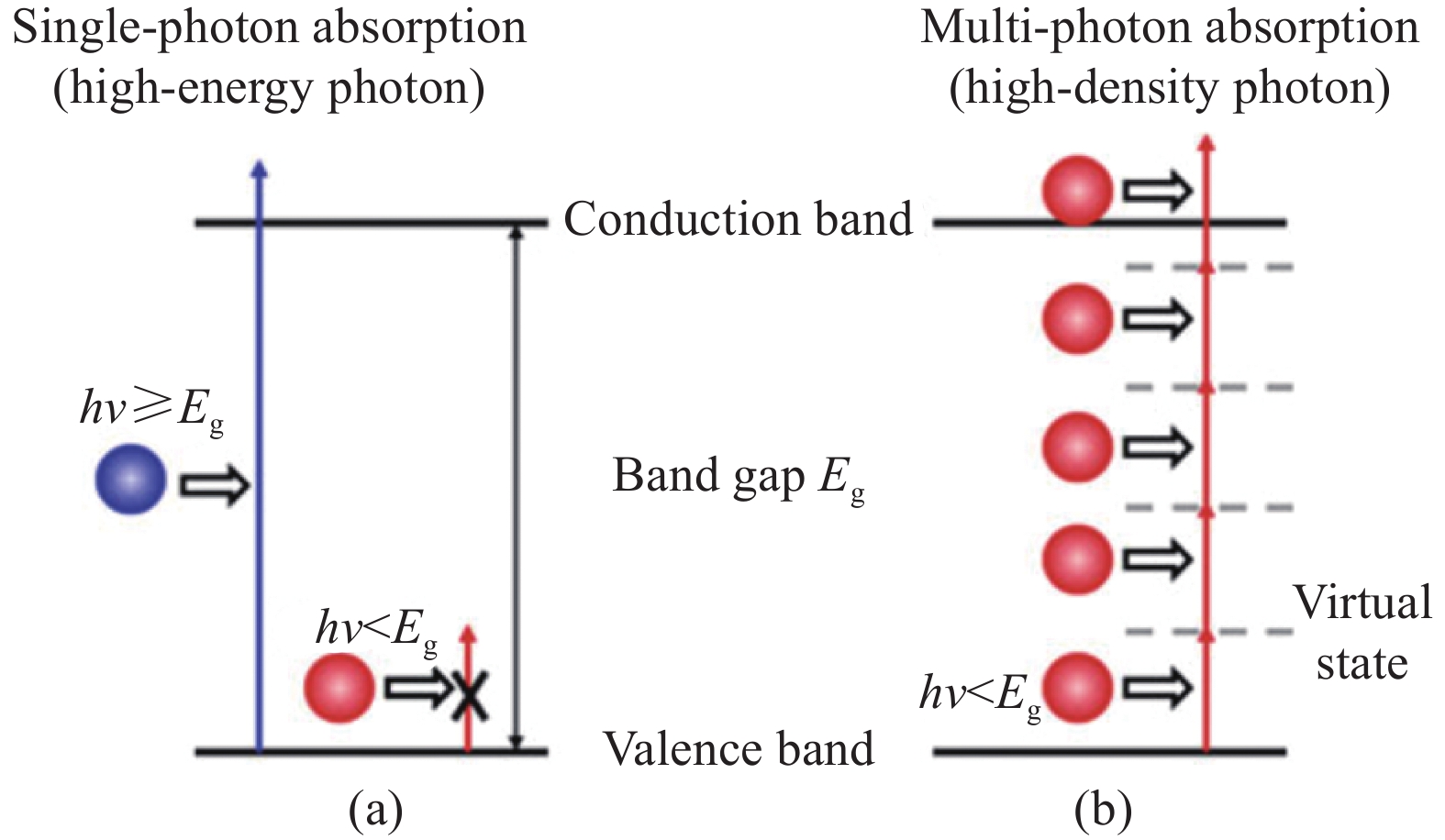
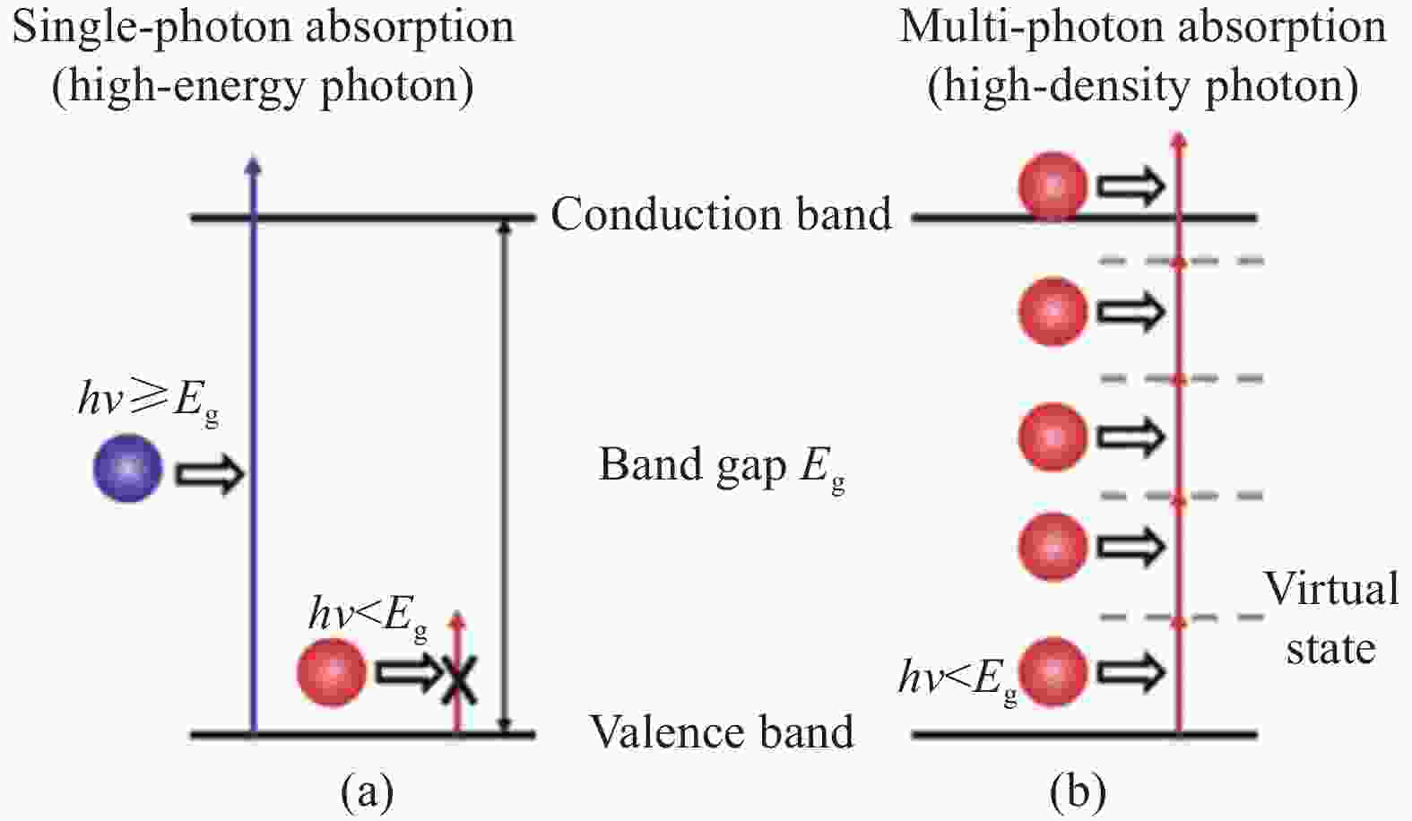
当飞秒激光照射到介质和宽带隙晶体等透明材料上时,由于激光峰值强度极高,会产生非线性吸收过程,从而引发强烈的光吸收。图2展示了电子激发过程的单光子和多光子吸收[13]。如图2 (a)所示,当单个光子能量大于材料带隙时会被吸收,并使一个电子被激发到导带;相反,当光子能量小于带隙时则不能激发电子,所以没有吸收。然而,当极高密度的光子入射到材料上时,即使能量小于材料带隙,一个电子也可以被同时吸收的多个光子激发(图2(b)),这种现象被称为多光子吸收。多光子吸收通常只能发生在激光焦点附近,在这种情况下,飞秒激光脉冲与透明材料之间的相互作用只能发生在焦点附近,此处的峰值强度最高。基于这一特点,飞秒激光可以实现透明材料内部的加工和改性,这是传统激光难以做到的。由此看来,飞秒激光与材料的非线性吸收是其能够满足三维成型、材料内部加工等特殊制造手段的根本原因。
由于极高峰值强度和非线性多光子吸收的特点,飞秒激光能够在透明材料内部以空间选择的方式进行三维加工,这也是飞秒激光另一显著特点之一[14-15]。非线性吸收发生的过程与激光强度密切相关,只有当激光强度超过特定的临界值时,才能有效地诱导非线性吸收发生,而这个临界值取决于加工材料和脉冲宽度。当具有足够脉冲能量的飞秒激光束聚焦在透明材料内部时,非线性吸收局限于材料内部焦点附近的区域,此时激光强度超过临界值。利用飞秒激光这一独特特性,再结合适当的刻蚀、退火工艺,就可以制备各类微光学部件、微流控器件和信息存储器件。目前,该技术已被广泛应用于光子器件、三维光波导、生物芯片制造及多维光存储等领域。
-
热影响区抑制和非线性多光子吸收的结合使得飞秒激光加工具有远超过衍射极限的空间分辨率。如1.1节所述,飞秒激光可以通过减少加工区域的热扩散来抑制热影响区的形成,由于热扩散可忽略不计,加工区域中的每一个像素几乎都与聚焦激光束的光斑大小相对应。光斑大小ω0由衍射极限决定(ω0=0.16λ/NA,其中λ是激光波长,NA为透镜的数值孔径)。因此,飞秒激光理论上可以进行不到半波长的空间分辨率的纳米制造。
利用非线性多光子吸收可以进一步提高空间分辨率。对于单光子吸收,其吸收激光能量的空间分布呈高斯分布。而多光子吸收的吸收能量分布要比单光子的分布更窄[16]。n光子吸收的有效光束尺寸ω可表示为:
$$ \omega = {\omega _0} / \sqrt n $$ 式中:ω0为聚焦激光束的实际光斑大小。由此可以看出多光子吸收可以克服激光束的衍射极限ω0,并达到亚衍射极限的分辨率。
此外,激光的阈值效应也可提升激光加工的分辨率。在包括烧蚀在内的很多加工过程中,激光强度存在一个阈值,只有超过此阈值,吸收光子能量才会发生反应。因此可以通过调节激光脉冲能量,使脉冲激光的能量尽量逼近阈值强度窗口,从而将加工尺寸减小到小于激光光斑尺寸,进一步提高加工精度。理论上,阈值效应对加工分辨率没有限制,通过对激光功率的稳定和控制,可以利用780 nm的飞秒激光获得比20 nm更好的分辨率[17]。但在实际应用中,飞秒激光输出功率的波动使得高分辨率的三维制造变得很困难,通常能够实现的空间分辨率为100~200 nm[18]。
-
飞秒激光加工按照加工方式可分为两种类型:飞秒激光直写加工和飞秒激光并行加工。飞秒激光直写通常通过单点曝光扫描,点动成线、线动成面,面动成体的方式实现微纳结构制备,具有加工灵活性强、空间分辨率高和可编程设计等优点,被广泛应用于制备光学波导、微透镜及各种三维微结构[19-21]。然而,由于飞秒激光直写的连续加工特性,其加工效率相对较低,在制备高精度、跨尺度的大尺寸微纳结构时受限。近年来,研究人员开发出各种高平均功率、高重复频率的飞秒激光器,极大地改善了这一问题,激光加工与干/湿法刻蚀相结合的复合制造技术也可以大幅度提升加工效率。为了从本质上提升激光加工的效率,飞秒激光并行加工技术受到了广泛关注。其中,激光分束并行加工、借助于空间光调制器的图案化加工以及全息激光加工等技术可以在实现大面积微结构制备的同时获得相对更高的效率。但其明显更加适用于周期性微纳结构制备,并不适用于任意复杂三维微结构的加工。在实际应用中,可以根据应用需求来选择合适的加工技术。
-
图3展示了一个典型的飞秒激光直写系统[22],主要由飞秒激光光源、光束控制/整形系统、显微物镜或用于产生紧聚焦光斑的非球面透镜,以及由计算机控制的用于样品三维平移的高精度XYZ平移台组成。由于飞秒激光的宽光谱特性,在加工聚焦时应尽量减小球差和色差。因此,通常选择商用显微物镜来进行加工,特别是在需要高空间分辨率时。另外,为了保证飞秒激光器的稳定运行,应该尽量减小激光器的脉冲宽度、脉冲能量和指向方向等参数的波动,飞秒激光器的输出能量在加工过程中应保持不变。而脉冲能量通常是通过半波片和偏振器来调节的,同时还可在偏振器后插入中性密度滤光片来实现更宽的可调谐范围。
飞秒激光直写制备二维和三维微结构通常有两种方法,一种是通过三维移动平台的运动,另一种是通过与变换平台相结合的振镜来实现的。前一种方法适用于阵列加工和对精度要求不高的应用[23-24],但对于大规模复杂微结构的快速、灵活微加工而言仍然十分缓慢。得益于高功率、高重复频率和小型化飞秒激光的高速发展[25-26],可以采用扫描振镜和压电片来实现高效率和高分辨率的微加工。利用双光子聚合技术可以简单地构建具有纳米精度的复杂三维微结构。在此基础上,研究者还可以调控三维结构内部的扫描参数,实现对微结构均匀性的调控。例如,如图4所示,吉林大学张永来教授课题组报道了一种“双三维”激光直写加工技术,成功实现了三维花瓣和机械手的制备,由于对内部结构进行了非均匀调控,所制备的结构可以被周围液体驱动,实现了从三维“雕塑”向“机器人”的转变[5]。飞秒激光烧蚀和改性可对多种材料进行加工,形成各种多级微结构、纳米沟槽和三维共振光学谐振腔等[27-29],广泛应用于浸润表面制备、光通信与生物医学领域。此外,飞秒激光直写技术正成为构建具有三维梯度密度的大规模多功能智能材料的一种极具吸引力的工具,可广泛应用于智能传感器、执行器和软体机器人的加工[30-31]。
-
为了使复杂微结构的制备过程更加高效灵活,研究人员开发了多种并行加工的方法,包括通过光学调制和衍射的多焦点并行处理、结构光、基于数字微镜器件的光刻技术(DMD)和液晶空间光调制器(LC-SLM)。其中,基于DMD和LC-SLM的方法可以动态调整加工图形以满足大多数应用的需求,因而得到了广泛的应用。
-
通过DMD调制形成任意二维图案,再通过合适的光化学、光物理机制将光场图案向材料图案整体转移,即可以实现大规模微结构阵列的高通量制备。需要注意的是,辐照在DMD上的光片应被整形成一个空间均匀的平头光束[32-33]。由于飞秒激光的高相干性,DMD上的微镜阵列也可作为衍射光栅。在不需要超分辨率的应用中,可以选择具有中等放大率的物镜来获得更大的视场和图案区域。由于DMD独特的优势,基于DMD的飞秒激光加工具有高通量、高对比度、快速响应和易于使用等优点。此外,DMD与数字化全息技术的结合可以实现光幅和相位的灵活调制,从而能够高效地打印各种复杂的高分辨率的三维结构[34-35]。最近,研究人员提出了一种基于DMD的时空同步聚焦的增材制造方法。该方法能够实现三维结构高通量超分辨率的并行加工。与现有的双光子聚合(TPP)技术相比,其打印速度提高了1000倍,轴向分辨率可达175 nm[36] 。
然而,入射激光在DMD上的衍射造成了显著的能量损失,因此飞秒激光的功率必须非常高。例如,当波长为800 nm的飞秒激光在DMD表面的入射角为57°、闪耀角为33°时,m=5阶的闪耀光束的能量为入射光束的75%。此外,激光从DMD表面的反射以及微镜之间的间隙同样会造成激光的能量损失。因此,DMD并行加工并不适用于需要较高功率的烧蚀加工,更适合于光聚合和激光改性加工。
-
与DMD的振幅调制不同,LC-SLM是通过改变液晶的分布来调节光场的相位,从而提高光能的利用率。LC-SLM与飞秒激光的结合是由日本德岛大学的研究人员首次提出的[37],由于其具有灵活加工的特性,基于空间光调制器的飞秒激光加工近年来受到了广泛的研究和关注。为了提高加工的精度、效率和分辨率,研究人员对空间光调制的全息算法和制造方法都进行了改进,以获得所需的图案化光束[38-39]。其中,结构化的激光微加工为构建特殊的微结构提供了一种快速灵活的解决方案。如图5所示,通过均匀的光强分布和可控参数的多样化,相位空间光调制器产生了马修光束,并制备出了复杂的微笼结构[40]。此外,利用非衍射的高质量光束可对各种形状的贝塞尔光束进行调制,用以制备高深宽比的微管、空心微螺旋结构和手性旋转结构[41-43]。

基于DMD和LC-SLM的飞秒激光加工可以快速、灵活地实现任意结构的图形加工。然而,高精度和大尺寸的同时实现是这两种方法在双光子聚合加工中面临的挑战。为了解决这一问题,Cheng等人提出了时空同步聚焦技术,可以在物镜聚焦处同时实现最短的激光脉冲宽度和最高的激光强度,从而有效提高了大规模三维微结构的分辨率[44-45]。通过这种方法,研究人员成功制备出了一个尺寸为3 cm×2.7 cm×1.1 cm的三维透明手,该透明手内部包含了完整的微通道血管系统[46]。
-
由于在整个脉冲持续时间内都具有良好的相干性,飞秒激光干涉为微加工提供了足够的能量密度。因此,可以在硬质材料表面或透明材料内部直接刻蚀或诱导大规模周期性微纳米结构。同时通过调节激光能量、入射角、干涉光束、聚焦透镜焦距、曝光时间及波长等参数,可对微纳米结构的周期、形态和尺寸进行调节。干涉光束一般由分光透镜和光栅产生。为了使激光干涉的加工系统更加简单、稳定并能实现灵活的图案化加工,研究者们进行了很多研究[43]。例如Li等人提出了一种基于迈克尔逊干涉仪的飞秒激光时空干涉方法,通过空间光调制器控制相位差,可使用单个激光脉冲在体材料上实现定制设计的灰度图案[47]。
直接飞秒激光干涉图案化加工已被广泛应用于纳米粒子尺寸分布裁剪、多功能金属表面修饰等领域[48]。利用分束器实现多光束干涉需要对光学系统进行精细调整,而利用光栅可以更简单地实现多光束干涉,且衍射产生的干涉区域大小与入射光的尺寸相近[49]。飞秒激光干涉具有一步加工、高效率、周期可控等优点,是构建周期性功能微纳米结构的可靠方法,目前已广泛应用在信息存储、生物医学工程和仿生智能表面等领域。
尽管与飞秒激光直写技术相比,激光并行加工已经在很大程度上提高了加工效率,然而受激光光源能量、激光加工系统条件等限制,其与光刻、压印等批量制造技术的效率相比依然相差很远。未来,飞秒激光加工效率的提升很大程度上依赖于高功率激光光源的发展和激光加工系统的改进。目前,激光加工技术主要用于特种材料加工与特殊器件制造。
-
如前所述,飞秒激光加工可以满足高精度三维结构制备、多材料微纳结构加工以及器件成型与集成的加工需求,因此,在各类微纳结构化功能部件的研制中展现出了很大的技术优势。在该节中,笔者针对一些典型应用领域的研究进展进行分类介绍。
-
微光学器件在显微成像、信息存储、光传感器等领域有着广泛的应用,利用飞秒激光加工可以实现各种二维或三维微光学器件的制备。微透镜阵列具有体积小、成本低、光学性能独特、易与其他系统集成等优点,在光调制、光学传感器、光学系统集成等领域发挥着不可替代的作用[50-53]。目前,基于飞秒激光加工的微透镜制备方法可分为增材制造、减材制造和激光诱导改性。微透镜阵列的增材制造主要是通过飞秒激光双光子聚合技术实现的。例如,吉林大学研究团队利用双光子聚合技术制备了一种基于仿生蛋白质的微透镜。该透镜在外界刺激下可动态调节焦距,同时具有独特的伸缩性、良好的生物相容性和生物可降解性[54]。该团队进一步利用激光加工技术制备了可变焦的仿生复眼,实现了大视场变焦成像的功能,如图6(a)所示[6]。在硬质材料上,飞秒激光减材制造也可以制备凹透镜阵列。为了实现较为光滑的透镜表面,这种制备方法通常需要与额外的刻蚀技术相结合,可以认为是一种复合制造技术。在湿法刻蚀和干法刻蚀的辅助下,飞秒激光烧蚀可在平面上加工各种类型的大规模微透镜,如凹面微透镜阵列、平面凸柱面微透镜阵列及透镜对透镜阵列等[55-56]。这类微透镜阵列不仅可以直接用于微光学系统,还可以做为模具实现微透镜整列的批量制造。例如,在熔点很高的蓝宝石表面制备微透镜阵列可以用于热熔玻璃的复制和仿生复眼的转写制备,如图6(b)[7]所示。增材制造和减材制造方法加工效率和灵活度高,适用于大多数材料,但制造工艺较为复杂。激光诱导改性的微透镜加工方法既不是增材也不是减材,它为规模化生产提供了一个合理的解决方案。例如,Zhang等人基于简单二维图案的激光诱导热变形制造了复杂的准三维表面结构,实现了万花筒式成像图案[57]。激光诱导改性方法所制备的微透镜阵列的表面粗糙度要明显高于基于增材和减材方法制备的微透镜。
光子晶体具有特殊的三维介电结构,可以通过产生带隙来阻止特定频率电磁波的传播。这种独特功能实现了集成光子学,展现其在波导、通信及激发分子化学反应中的应用潜力[58-60]。飞秒激光的高精度、真三维加工能力及可设计加工等优点使其已广泛应用在光子晶体加工方面。近几十年来,研究者们对利用飞秒激光制备光子晶体进行了深入的研究。利用飞秒激光多光子聚合制备的光子晶体其光子带隙已经从中红外扩展到可见光[61];通过飞秒激光选择性擦除可制备三维铌酸锂非线性光子晶体[62],同时通过飞秒激光的非线性全息可实现非线性光束整形,与传统二维技术相比,其制造效率提高了两个数量级。此外,飞秒激光直写已经成为光纤加工、特种光纤创新和应用的重要途径。例如,利用飞秒激光处理可在光纤芯和包层上进行微结构制备,从而实现了多功能光纤传感器[63];目前,研究者们已经在各类光纤上利用飞秒激光加工技术制备了光栅、悬臂梁、光学微腔等典型结构,实现了温度、压力、应力等多种信号的敏感探测[64]。
飞秒激光加工的另一个重要的应用是光栅和光波导加工。例如,Liu等人提出了一种飞秒激光光刻和后续反应离子刻蚀相结合的技术,在蓝宝石上制造出了闪耀光栅。借助飞秒激光光刻任意构建自由曲面三维微纳米结构的优势,通过反应离子刻蚀技术可将各种高度和周期的闪耀光栅转移到蓝宝石上[65];Hou等人将飞秒激光直写光波导技术与传统的超导纳米线结合在一起,制备了一种新型的飞秒激光直写波导耦合单光子探测器,可实现对阵列单光子的检测[66];He等人展示了利用飞秒激光直写技术在多模无芯光纤中制备单模螺旋布拉格光栅波导的方法[67],这种飞秒激光螺旋直写方法为创建布拉格光栅波导提供了一种简单的“一步法”,并且适用于多种器件,如蓝宝石光纤传感器、硅基光子集成电路和单片波导激光器等。
-
近年来,微流体器件由于其高活性、高敏感性和安全环保等一系列优点受到了广泛的关注和研究。微流体器件是芯片上实验室的关键组成部分。芯片上实验室是集成了生物、化学、光学、医学等学科实验室功能的微型实验室,可用于反应、检测、分析、分离和生化材料合成等实验,具有高敏高效、低消耗等优点[68]。生物芯片的广泛应用也刺激了微流体器件制造技术的发展,例如紫外光、软光刻、X射线光刻及纳米压印等方法都已成功用于平面微流控通道的构建[22]。然而这些方法难以制备具有复杂三维拓扑结构的精细微流控芯片。飞秒激光加工技术的三维加工能力、高分辨率和高精度等优点使其成为制造三维微流控芯片的一种强有力的工具。
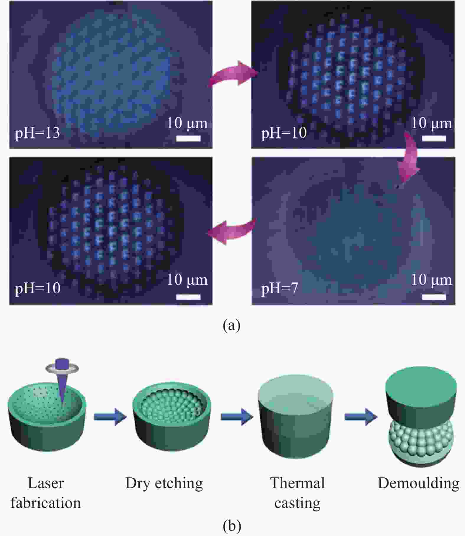
飞秒激光可在多种材料内部进行微纳结构加工的能力使得目前微流体器件的制备材料体系十分多样化,可以满足不同应用场景的需求。最常见的制备材料为玻璃和聚合物材料[69-72]。Cheng课题组展示了利用飞秒激光直写在多孔玻璃内制备的三维微流体通道。通过在水下对多孔玻璃进行飞秒激光烧蚀以及随后的高温退火,可在玻璃内制造出长度和几何形状任意的微通道[69]。该方法无需额外的堆叠和键合程序,可实现三维微流控系统的快速成型,提高了制备效率、灵活性和制造精度,降低了制造成本。Tanaka等人提出了一种利用飞秒激光加工制备全玻璃的超薄柔性多层微流控芯片的方法[70]。该微流控芯片由上下两层具有出入孔的玻璃基板和中间层具有微通道的玻璃基板组成,其厚度仅为12 μm。该制造方法明显降低了柔性玻璃微流体器件的厚度限制,并为制造超薄玻璃微流控器件提供了一种强有力的技术支撑。Roth等人报道了一种利用飞秒激光在聚甲基丙烯酸甲酯(PMMA)材料内部直接产生三维微通道的方法,如图7所示[71]。PMMA中的微通道是通过两步过程构建的:首先飞秒激光辐照样品,聚焦体积周围的非线性吸收触发PMMA材料改性,将焦点在材料内部进行三个维度的平移以获得三维通道结构;随后将样品进行退火,改性区域在退火温度下发生降解,在样品内部膨胀并形成了微流体通道。通过控制激光功率、写入速度和扫描次数,可以调节微通道的高度、宽度和长宽比等尺寸,从而实现任意三维微通道结构的构建。
此外,在面对一些特殊的应用需求,例如在高压和高温条件下工作的微流控芯片,传统材料由于其自身材料特性的限制无法满足这类需求。目前,一些具有优越机械性能的材料,如蓝宝石和金刚石已被研究者们开发并用于微流体器件的制备中[73-74]。Aryana等人利用飞秒激光在蓝宝石内部刻蚀出各种几何形状的微流控通道,在键合后形成密封的微流控装置[73]。通过空气和乙醇的自吸实验和破坏性机械实验证实了所制备通道的机械强度和密封性。使用飞秒激光进行光学微加工和键合为蓝宝石基微流控系统的制备提供了一个可集成的途径,同时为创造可在极端环境下观察流体动力学的机械和化学抵抗性设备提供了可能性。
-
飞秒激光能够构建多种周期、形貌不一的微纳米结构[75-76]。其中,激光诱导的周期性表面结构,即LIPSS结构是研究最广泛的结构之一。LIPSS结构被认为是入射激光束与表面散射或反射的光相干涉形成的,也被称为表面波纹。目前,利用飞秒激光可在金属、半导体、聚合物和电介质等多种材料表面诱导出LIPSS结构[77-80],其空间周期远小于激光波长,波纹方向取决于所加工材料的类型。对于金属和半导体,LIPSS结构通常垂直于激光束的偏振方向,而对于电介质,其方向既可以是垂直的,也可以是平行的:通过将激光束变为椭圆偏振,可以使波纹发生旋转;而对于圆偏振光束,则会产生均匀分布的凸点。另外,双光束辐照的方法也可以改变LIPSS结构的方向。通过精确控制两个入射脉冲的相位差,可使在硅表面形成的LIPSS方向旋转90°[81]。LIPSS结构的形成机制已被广泛研究,包括二次谐波的产生[82]、表面等离子体激元与飞秒激光的干涉[83]、纳米等离子体的形成[84]和表面不稳定性的自组织[85]等,然而目前尚无统一的结论。
LIPSS结构在很多领域都有着潜在的应用,如降低微纳米组件间的粘附力、提高浸润性、增加薄膜和医疗植入物间的附着力以及表面着色等。在不锈钢表面形成的LIPSS结构可用来进行彩印[86],其颜色效应是通过表面周期性纳米结构的光衍射实现的。依赖于偏振方向的纳米结构取向的空间控制能够在金属表面成功压印出彩色图像。Jiang等人受具有美丽结构色和独特疏水特性的蝴蝶翅膀启发,利用飞秒激光在铜箔表面制备了纳米级LIPSS结构,如图8所示[8]。该结构与激光扫描出的微米条纹结合构成了多级微纳米复合结构,在展现了结构色的同时也赋予了铜箔超疏水特性。进一步,以该结构化铜箔为基底,通过CVD方法制备出了具有相同结构的石墨烯薄膜。

另一种有趣且实用的结构是由飞秒激光在卤素气体(如SF6和Cl2)中进行数百次脉冲辐照形成的、微米级准有序的锥形阵列[87-88]。所形成的微锥结构的大小和形状取决于激光能量密度、波长、脉冲持续时间以及所处气体环境。这种微锥结构可以在不同的材料表面产生,并展示出了不同的功能性。例如研究人员利用飞秒激光在硅片表面诱导出微锥结构,由于该结构大大减少了入射光的反射,因而使硅表面由原来的金属镜面变成了深哑光黑色,称为黑硅[89]。此外,利用飞秒激光还可加工出多孔的网状结构,用于调控材料表面的浸润特性。Yong等人利用飞秒激光在尼龙6材料表面制备了多孔的网状微纳结构,可用于构建超滑表面,应用在液滴操控、抗结冰、防污垢等领域[90]。
-
在过去的20年里,飞秒激光已经成为生物医学工程领域的主流加工方法,并在临床实践中占有一席之地。在不破坏细胞活力的情况下,在亚细胞水平上改变生物介质是飞秒激光在生物医学研究中的突出特点之一,同时高精度和适度的热影响区是飞秒激光应用于临床研究的主要因素,尤其是眼科。例如,飞秒激光目前已经广泛应用于视力矫正手术、前板层角膜移植、角膜植入物通道创建以及白内障手术中。激光原位角膜磨平术是一种视力矫正手术,该手术通过机械切片机形成角膜瓣,并用准分子激光光消融基质组织,其中飞秒激光被引入以取代机械微角膜刀,从而实现更加精准有效的手术效果。与机械角膜成形术相比,飞秒激光生成的角膜瓣具有很多优点,包括在手术过程中的高精度、更均匀的厚度以及降低眼压和感染风险等[91-92]。在下一代的小切口晶状体摘除术中,仅需用飞秒激光在角膜内部直接创建通道就可重塑角膜,而无需去除角膜最外层的上皮组织。
飞秒激光在生物医学中另一项独特应用是医疗微设备的制造,如生物微型支架、生物显微成像以及体内给药系统等[93-95]。研究人员报道了一种利用双光子聚合技术制备的可植入体内的微型止回阀门,该元件用于防止人体静脉中的血液发生逆流[94]。该阀门在开启时血液向前流动,而在关闭时可以有效地防止血液回流。同时,由于双光子聚合加工的灵活特性,可以根据患者不同的要求调整设计尺寸,从而改变微型阀门的尺寸,而整个制造过程仅需几分钟。此外,利用飞秒激光对生物相容性材料进行加工也可用于制备生物微型支架,这类微型支架在细胞组织再生、血管重构和形成、细胞附着转移等方面展现出了巨大的应用潜力。
-
超快激光具有超快、超强和超精细等特点,将超快激光用作加工工具可以打破传统微纳制造的局限,通过激光与材料的非线性作用,实现特殊材料、复杂结构和特种器件的激光制造,开辟了特种微纳制造的新途径。该文聚焦飞秒激光微纳加工技术,综述了飞秒激光加工的技术特点、材料加工方式以及前沿应用案例。作为前沿加工技术,飞秒激光加工具有热影响区小、与材料相互作用呈非线性过程、超出衍射极限的高分辨率加工等特点,可以实现对各种材料的高质量、高精度微纳米加工和三维微纳结构制造。
飞秒激光对材料的加工方式灵活多样,既可实现增材、减材和等材制造,又能够以激光直写和激光并行加工的方式制备微纳结构。其中,飞秒激光直写通常用于复杂、不规则的微纳结构加工,具有较高的空间分辨率、加工灵活性和自由度,然而鉴于其逐点加工的技术特点,加工效率较低;飞秒激光并行加工包括基于数字微镜器件的光刻技术、空间光调制器和激光干涉加工等方法,具有较高的加工效率,但无法加工任意三维微结构。目前,飞秒激光已经广泛应用于多个前沿科学领域:利用飞秒激光可以制备各种微光学器件,如微透镜阵列、仿生复眼、光波导和超表面等;利用其高精度、高分辨率和三维加工能力,飞秒激光可以制备或集成微加热器、微搅拌器、微筛分部件和三维微流控通道等微流控、光流控芯片;此外,飞秒激光还可以制备不同类型的表面微纳米结构,实现抗反射、增透、超疏水、抗结冰等功能;不仅如此,飞秒激光在生物医学领域也得到了前沿应用,在如眼科手术、生物微型支架、细胞培养基底和生物显微成像等领域中,展现出了广阔的应用前景。
近年来,飞秒激光加工技术得到了飞速的发展,加工精度下探至几十纳米,加工效率呈数量级提升;飞秒激光瞬时功率大,可以与大多数材料发生非线性相互作用,对可加工材料具有普适性,可以对包括金属、碳材料、氧化物、聚合物、玻璃、蓝宝石、金刚石等多种材料进行加工;同时,飞秒激光可实现高精度、真三维加工,这是很多微纳加工技术不具备的特性;目前,飞秒激光加工应用领域逐年扩增,除了上述微光学、微流控、多功能微纳米结构及生物医学工程应用之外,在一些新兴领域也发挥着巨大的作用,例如,超表面制备、微纳机器人制造和多维光信息存储等。尽管如此,飞秒激光加工技术仍然是一项新颖的技术,面向未来,仍然存在诸多的难点需要攻克。例如,飞秒激光与物质间的相互作用机制十分复杂,针对不同材料加工中共性和个性化的科学问题,仍需要研究者通过建立不同的物理模型来给出解释;飞秒激光加工技术的进步也同时依赖激光光源的不断发展,大功率的飞秒激光光源是实现飞秒激光的加工质量、加工效率和加工分辨率提升的根本动力;对于飞秒激光加工来讲,加工精度、加工效率和加工尺度之间一直存在矛盾。近几年,飞秒激光加工精度已经提升至纳米量级。而以并行加工策略为代表的新技术也一定程度上提升了制备效率。相比之下,飞秒激光的加工尺度还有待提高,受高精度三维移动平台和光学系统的限制,加工尺度通常较小,这严重限制了其实际应用。实现加工尺度从微米、毫米尺度到宏观大面积(厘米、米)的拓展是飞秒激光加工技术未来的发展方向之一,这很大程度上依赖于更加先进的飞秒激光加工系统。此外,飞秒激光在一些新兴领域的应用还值得研究者们的不断探索。笔者相信飞秒激光加工技术未来一定会有更广阔的应用舞台。
Progress and application of nonlinear laser manufacturing (Invited)
-
摘要: 超快激光是指脉冲宽度极窄的激光,其瞬时功率极高,与物质之间的相互作用呈现出非线性、非平衡、多尺度的状态。超快激光具有超快(脉冲持续时间短)、超强(瞬时功率高)、超精细(加工结构精细)等特点,由此实现的非线性激光制造技术可以打破传统微纳制造的局限,实现各类难加工材料和复杂微纳结构的超精细制造,精度可达亚微米至纳米量级,在微光学、生物医学、智能电子器件等前沿领域体现出了独特的应用价值。文中主要聚焦飞秒激光微纳加工技术前沿,简要概括了飞秒激光加工的特点;介绍了飞秒激光加工的主要技术手段,包括飞秒激光直写和飞秒激光并行加工;讨论了飞秒激光加工技术的前沿应用领域,如微纳光学器件、微流体器件、多功能结构化表面、生物医学工程等;最后,对飞秒激光加工制造技术未来的发展趋势和研究方向进行展望。Abstract: Ultrafast lasers refer to lasers with very narrow widths. Ultrafast laser has extremely high instantaneous power, and its interaction with matter presents a non-linear, nonequilibrium and multi-scale state. With the unique characteristics of ultrafast(short pulse duration), ultrahigh (high instantaneous power) and ultrafine (fine processing structure), the realized nonlinear laser manufacturing technology can break the limitations of traditional micro-nano manufacturing and realize the ultrafine processing of various difficult-to-machine materials and complex micronano structures. It demonstrates unique application value in frontier fields such as microoptics, biomedicine, and intelligent electronic devices with precision ranging from sub-micron to nanoscale. The frontiers of femtosecond laser micro/nano machining technology was focused on. Firstly, the processing characteristics of femtosecond laser technology and the main processing methods were introduced, including femtosecond laser direct writing and femtosecond laser parallel processing. Then, the frontier application fields of femtosecond laser processing technology were discussed, such as micro-nano optical devices, microfluidic devices, multifunctional structured surfaces and biomedical engineering. Finally, the future development trend and research direction of femtosecond laser processing technology were prospected.
-
Key words:
- ultrafast laser /
- femtosecond laser /
- nonlinear interaction /
- micro-nano manufacturing /
- 3D fabrication
-


-
[1] Strickland D, Mourou G. Compression of amplified chirped optical pulses [J]. Optics Communications, 1985, 55(6): 447-449. doi: 10.1016/0030-4018(85)90151-8 [2] Spence D E, Kean P N, Sibbett W. 60-fsec pulse generation from a self-mode-locked Ti: sapphire laser [J]. Optics Letters, 1991, 16(1): 42. doi: 10.1364/OL.16.000042 [3] Wang F Y, Zou T T, Xin W, et al. Control of the wettability of graphene oxide surface with femtosecond laser irradiation (Invited) [J]. Infrared and Laser Engineering, 2020, 49(12): 20201064. (in Chinese) doi: 10.3788/IRLA20201064 [4] Yue D M, Sun H L, Yang X, et al. Annular drilling process and quality control neural network model of stainless steel micro-hole with femtosecond laser [J]. Infrared and Laser Engineering, 2021, 50(10): 20200446. (in Chinese) doi: 10.3788/IRLA20200446 [5] Zhang Y L, Tian Y, Wang H, et al. Dual-3D femtosecond laser nanofabrication enables dynamic actuation [J]. ACS Nano, 2019, 13(4): 4041-4048. doi: 10.1021/acsnano.8b08200 [6] Ma Z C, Hu X Y, Zhang Y L, et al. Smart compound eyes enable tunable imaging [J]. Advanced Functional Materials, 2019, 29(38): 1903340. doi: 10.1002/adfm.201903340 [7] Liu X Q, Yang S N, Yu L, et al. Rapid engraving of artificial compound eyes from curved sapphire substrate [J]. Advanced Functional Materials, 2019, 29(18): 1900037. doi: 10.1002/adfm.201900037 [8] Jiang H B, Zhang Y L, Liu Y, et al. Bioinspired few-layer graphene prepared by chemical vapor deposition on femtosecond laser-structured Cu foil [J]. Laser & Photonics Reviews, 2016, 10(3): 441-450. [9] Lei S T, Zhao X, Yu X M, et al. Ultrafast laser applications in manufacturing processes: A state-of-the-art review [J]. Journal of Manufacturing Science and Engineering, 2020, 142(3): 031005. doi: 10.1115/1.4045969 [10] Chichkov B N, Momma C, Nolte S, et al. Femtosecond, picosecond and nanosecond laser ablation of solids [J]. Applied Physics A, 1996, 63(2): 109-115. doi: 10.1007/BF01567637 [11] Eaton S M, Zhang H B, Herman P R. Heat accumulation effects in femtosecond laser-written waveguides with variable repetition rate [J]. Optics Express, 2005, 13(12): 4708-4716. doi: 10.1364/OPEX.13.004708 [12] Eaton S M, Zhang H, Ng M L, et al. Transition from thermal diffusion to heat accumulation in high repetition rate femtosecond laser writing of buried optical waveguides [J]. Optics Express, 2008, 16(13): 9443-9458. doi: 10.1364/OE.16.009443 [13] Sugioka K, Cheng Y. Femtosecond laser three-dimensional micro- and nanofabrication [J]. Applied Physics Reviews, 2014, 1(4): 041303. doi: 10.1063/1.4904320 [14] Davis K M, Miura K, Sugimoto N, et al. Writing waveguides in glass with a femtosecond laser [J]. Optics Letters, 1996, 21(21): 1729-1731. doi: 10.1364/OL.21.001729 [15] Glezer E N, Milosavljevic M, Huang L, et al. Three-dimensional optical storage inside transparent materials [J]. Optics Letters, 1996, 21(24): 2023-2025. doi: 10.1364/OL.21.002023 [16] Sugioka K, Cheng Y. Femtosecond Laser 3 D Micromachining for Microfluidic and Optofluidic Applications [M]//Springer Briefs in Applied and Technology. London: Springer, 2014: 24-25. [17] Tan D F, Li Y, Qi F J, et al. Reduction in feature size of two-photon polymerization using SCR500 [J]. Applied Physics Letters, 2007, 90(7): 071106. doi: 10.1063/1.2535504 [18] Kawata S, Sun H B, Tanaka T, et al. Finer features for functional microdevices [J]. Nature, 2001, 412(6848): 697-698. doi: 10.1038/35089130 [19] Sugioka K, Cheng Y, Midorikawa K. Three-dimensional micromachining of glass using femtosecond laser for lab-on-a-chip device manufacture [J]. Applied Physics A-Materials Science & Processing, 2005, 81(1): 1-10. [20] Straub M, Afshar M, Feili D, et al. Periodic nanostructures on Si(100) surfaces generated by high-repetition rate sub-15 fs pulsed near-infrared laser light [J]. Optics Letters, 2012, 37(2): 190-192. doi: 10.1364/OL.37.000190 [21] Li L J, Fourkas J T. Multiphoton polymerization [J]. Materials Today, 2007, 10(6): 30-37. doi: 10.1016/S1369-7021(07)70130-X [22] Zhang Y L, Chen Q D, Xia H, et al. Designable 3D nanofabrication by femtosecond laser direct writing [J]. Nano Today, 2010, 5(5): 435-448. doi: 10.1016/j.nantod.2010.08.007 [23] Ye S, Cao Q, Wang Q S, et al. A highly efficient, stable, durable, and recyclable filter fabricated by femtosecond laser drilling of a titanium foil for oil-water separation [J]. Scientific Reports, 2016, 6: 37591. doi: 10.1038/srep37591 [24] Shi X S, Li X, Jiang L, et al. Femtosecond laser rapid fabrication of large-area rose-like micropatterns on freestanding flexible graphene films [J]. Scientific Reports, 2015, 5: 17557. doi: 10.1038/srep17557 [25] Marchese S V, Baer C R E, Engqvist A G, et al. Femtosecond thin disk laser oscillator with pulse energy beyond the 10-microjoule level [J]. Optics Express, 2008, 16(9): 6397-6407. doi: 10.1364/OE.16.006397 [26] Kleinbauer J, Eckert D, Weiler S, et al. 80 W ultrafast CPA-free disk laser [C]//Proceedings of SPIE, 2008, 6871 : 68711B. [27] Yong J L, Chen F, Li M J, et al. Remarkably simple achievement of superhydrophobicity, superhydrophilicity, underwater superoleophobicity, underwater superoleophilicity, underwater superaerophobicity, and underwater superaerophilicity on femtosecond laser ablated PDMS surfaces [J]. Journal of Materials Chemistry A, 2017, 5(48): 25249-25257. doi: 10.1039/C7TA07528F [28] Lin J T, Yu S J, Ma Y G, et al. On-chip three-dimensional high-Q microcavities fabricated by femtosecond laser direct writing [J]. Optics Express, 2012, 20(9): 10212-10217. doi: https://doi.org/10.1364/OE.20.010212 [29] Xu H L, Sun H B. Femtosecond laser 3D fabrication of whispering-gallery-mode microcavities [J]. Science China-Physics Mechanics & Astronomy, 2015, 58(11): 114202. doi: https://doi.org/10.1007/s11433-015-5720-5 [30] Huang T Y, Huang H W, Jin D D, et al. Four-dimensional micro-building blocks [J]. Science Advances, 2020, 6(3): eaav8219. doi: 10.1126/sciadv.aav8219 [31] Lv C, Sun X C, Xia H, et al. Humidity-responsive actuation of programmable hydrogel microstructures based on 3D printing [J]. Sensors and Actuators B-Chemical, 2018, 259: 736-744. doi: 10.1016/j.snb.2017.12.053 [32] Mills B, Grant-Jacob J A, Feinaeugle M, et al. Single-pulse multiphoton polymerization of complex structures using a digital multimirror device [J]. Optics Express, 2013, 21(12): 14853-14858. doi: 10.1364/OE.21.014853 [33] Mills B, Heath D J, Feinaeugle M, et al. Laser ablation via programmable image projection for submicron dimension machining in diamond [J]. Journal of Laser Applications, 2014, 26(4): 041501. doi: 10.2351/1.4893749 [34] Wang D, Wen C Y, Chang Y N, et al. Ultrafast laser-enabled 3D metal printing: A solution to fabricate arbitrary submicron metal structures [J]. Precision Engineering, 2018, 52: 106-111. doi: https://doi.org/10.1016/j.precisioneng.2017.11.015 [35] Guo Y M, Wang Y, Hu Q L, et al. High-resolution femtosecond laser beam shaping via digital holography [J]. Optics Letters, 2019, 44(4): 987-990. doi: 10.1364/OL.44.000987 [36] Saha S K, Wang D, Nguyen V H, et al. Scalable submicrometer additive manufacturing [J]. Science, 2019, 366(6461): 105-109. doi: 10.1126/science.aax8760 [37] Hasegawa S, Hayasaki Y, Nishida N. Holographic femtosecond laser processing with multiplexed phase Fresnel lenses [J]. Optics Letters, 2006, 31(11): 1705-1707. doi: 10.1364/OL.31.001705 [38] Zhang C C, Hu Y L, Du W Q, et al. Optimized holographic femtosecond laser patterning method towards rapid integration of high-quality functional devices in microchannels [J]. Scientific Reports, 2016, 6: 33281. doi: 10.1038/srep33281 [39] Xu B, Ji S Y, Pan D, et al. Hybrid femtosecond laser fabrication of a size-tunable microtrap chip with a high-trapping retention rate [J]. Optics Letters, 2020, 45(5): 1071-1074. doi: 10.1364/OL.386095 [40] Wang C W, Yang L, Hu Y L, et al. Femtosecond mathieu beams for rapid controllable fabrication of complex microcages and application in trapping microobjects [J]. ACS Nano, 2019, 13(4): 4667-4676. doi: 10.1021/acsnano.9b00893 [41] Ji S Y, Yang L, Zhang C C, et al. High-aspect-ratio microtubes with variable diameter and uniform wall thickness by compressing Bessel hologram phase depth [J]. Optics Letters, 2018, 43(15): 3514-3517. doi: 10.1364/OL.43.003514 [42] Xin C, Yang L, Li J W, et al. Conical hollow microhelices with superior swimming capabilities for targeted cargo delivery [J]. Advanced Materials, 2019, 31(25): 1808226. doi: 10.1002/adma.201808226 [43] Ni J C, Wang C W, Zhang C C, et al. Three-dimensional chiral microstructures fabricated by structured optical vortices in isotropic material [J]. Light: Science & Applications, 2017, 6: e17011. [44] Chu W, Tan Y X, Wang P, et al. Centimeter-height 3D printing with femtosecond laser two-photon polymerization [J]. Advanced Materials Technologies, 2018, 3(5): 1700396. doi: 10.1002/admt.201700396 [45] Wang P, Chu W, Li W B, et al. Three-dimensional laser printing of macro-scale glass objects at a micro-scale resolution [J]. Micromachines, 2019, 10(9): 565. doi: 10.3390/mi10090565 [46] Lin Z J, Xu J, Song Y P, et al. Freeform microfluidic networks encapsulated in laser-printed 3D macroscale glass objects [J]. Advanced Materials Technologies, 2020, 5(2): 1900989. doi: 10.1002/admt.201900989 [47] Li B H, Jiang L, Li X W, et al. Flexible gray-scale surface patterning through spatiotemporal-interference-based femto-second laser shaping [J]. Advanced Optical Materials, 2018, 6(24): 1801021. doi: 10.1002/adom.201801021 [48] Jurkeviciute A, Klimaite G, Tamulevicius T, et al. Tailoring of silver nanoparticle size distributions in hydrogenated amorphous diamond-like carbon nanocomposite thin films by direct femtosecond laser interference patterning [J]. Advanced Engineering Materials, 2020, 22(3): 1900951. doi: 10.1002/adem.201900951 [49] Jia X, Jia T Q, Zhang S A, et al. Manipulation of cross-linked micro/nanopatterns on ZnO by adjusting the femtosecond-laser polarizations of four-beam interference [J]. Applied Physics A-Materials Science & Processing, 2014, 114(4): 1333-1338. [50] Shrestha S, Overvig A C, Lu M, et al. Broadband achromatic dielectric metalenses [J]. Light: Science & Applications, 2018, 7: 85. [51] Nagelberg S, Zarzar L D, Nicolas N, et al. Reconfigurable and responsive droplet-based compound micro-lenses [J]. Nature Communications, 2017, 8: 14673. doi: 10.1038/ncomms14673 [52] Thiele S, Arzenbacher K, Gissibl T, et al. 3D-printed eagle eye: Compound microlens system for foveated imaging [J]. Science Advances, 2017, 3(2): e1602655. doi: 10.1126/sciadv.1602655 [53] Su Y H, Qin T T, Xu B, et al. Patterned microlens processed using two-photon polymerization of femtosecond laser and its imaging test [J]. Optics and Precision Engineering, 2020, 28(12): 2629-2635. (in Chinese) doi: 10.37188/OPE.20202812.2629 [54] Sun Y L, Li Q, Sun S M, et al. Aqueous multiphoton lithography with multifunctional silk-centred bio-resists [J]. Nature Communications, 2015, 6: 8612. doi: 10.1038/ncomms9612 [55] Yang Q, Tong S Y, Chen F, et al. Lens-on-lens microstructures [J]. Optics Letters, 2015, 40(22): 5359-5362. doi: 10.1364/OL.40.005359 [56] Sohn I B, Choi H K, Noh Y C, et al. Laser assisted fabrication of micro-lens array and characterization of their beam shaping property [J]. Applied Surface Science, 2019, 479: 375-385. doi: 10.1016/j.apsusc.2019.02.083 [57] Zhang H R, Yang F Y, Dong J J, et al. Kaleidoscopic imaging patterns of complex structures fabricated by laser-induced deformation [J]. Nature Communications, 2016, 7: 13743. doi: 10.1038/ncomms13743 [58] Bauser H C, Bukowsky C R, Phelan M, et al. Photonic crystal waveguides for >90% light trapping efficiency in luminescent solar concentrators [J]. ACS Photonics, 2020, 7(8): 2122-2131. doi: 10.1021/acsphotonics.0c00593 [59] Li M X, Ling J W, He Y, et al. Lithium niobate photonic-crystal electro-optic modulator [J]. Nature Communications, 2020, 11(1): 4123. doi: 10.1038/s41467-020-17950-7 [60] Fenzl C, Hirsch T, Wolfbeis O S. Photonic crystals for chemical sensing and biosensing [J]. Angewandte Chemie-International Edition, 2014, 53(13): 3318-3335. doi: 10.1002/anie.201307828 [61] Liu Z S, Zhou X Y, Jia X H, et al. Visible light perovskite-coated photonic crystal surface-emitter on SOI [J]. Semiconductor Science and Technology, 2020, 35(7): 075019. doi: 10.1088/1361-6641/ab8840 [62] Wei D Z, Wang C W, Wang H J, et al. Experimental demonstration of a three-dimensional lithium niobate nonlinear photonic crystal [J]. Nature Photonics, 2018, 12(10): 596-600. doi: 10.1038/s41566-018-0240-2 [63] Kalli K, Theodosiou A, Ioannou A, et al. Femtosecond laser processing of optical fibres for novel sensor development [C]//Proceedings of the 25 th International Conference on Optical Fibre Sensors (OFS), 2017: 10323. [64] Ming X Y, Guo Q, Xue Z K, et al. A femtosecond laser-inscribed fine-core long-period grating with low temperature sensitivity [J]. Chinese Optics, 2020, 13(4): 737-744. (in Chinese) doi: 10.37188/CO.2020-0015 [65] Liu X Q, Cheng R, Zheng J X, et al. Wear-resistant blazed gratings fabricated by etching-assisted femtosecond laser lithography [J]. Journal of Lightwave Technology, 2021, 39(14): 4690-4694. doi: 10.1109/JLT.2021.3066976 [66] Hou X T, Xu X Y, Xu G Z, et al. Waveguide-coupled superconducting nanowire single-photon detectors based on femtosecond laser direct writing [J]. Optics Express, 2021, 29(5): 7746-7756. doi: 10.1364/OE.419724 [67] He J, He J, Xu X Z, et al. Single-mode helical Bragg grating waveguide created in a multimode coreless fiber by femtosecond laser direct writing [J]. Photonics Research, 2021, 9(10): 2052-2059. doi: 10.1364/PRJ.434719 [68] Song Y J, Zhang Y Q, Bernard P E, et al. Multiplexed volumetric bar-chart chip for point-of-care diagnostics [J]. Nature Communications, 2012, 3: 1283. doi: 10.1038/ncomms2292 [69] Liao Y, Song J X, Li E, et al. Rapid prototyping of three-dimensional microfluidic mixers in glass by femtosecond laser direct writing [J]. Lab on a Chip, 2012, 12(4): 746-749. doi: 10.1039/c2lc21015k [70] Yalikun Y, Hosokawa Y, Iino T, et al. An all-glass 12 μm ultra-thin and flexible microfluidic chip fabricated by femtosecond laser processing [J]. Lab on a Chip, 2016, 16(13): 2427-2433. doi: 10.1039/C6LC00132G [71] Roth G L, Esen C, Hellmann R. Femtosecond laser direct generation of 3 D-microfluidic channels inside bulk PMMA [J]. Optics Express, 2017, 25(15): 18442-18450. doi: 10.1364/OE.25.018442 [72] Xu B, Shi Y, Lao Z X, et al. Real-time two-photon lithography in controlled flow to create a single-microparticle array and particle-cluster array for optofluidic imaging [J]. Lab on a Chip, 2018, 18(3): 442-450. doi: 10.1039/C7LC01080J [73] Elgohary A, Block E, Squier J, et al. Fabrication of sealed sapphire microfluidic devices using femtosecond laser micromachining [J]. Applied Optics, 2020, 59(30): 9285-9291. doi: 10.1364/AO.400184 [74] Bharadwaj V, Jedrkiewicz O, Hadden J P, et al. Femtosecond laser written photonic and microfluidic circuits in diamond [J]. Journal of Physics-Photonics, 2019, 1(2): 022001. doi: 10.1088/2515-7647/ab0c4e [75] Zhang C Y, Liu H Y, Man W Q, et al. Femtosecond laser induced surface micro-and nano-structures by orthogonal scanning processing [J]. Optics and Precision Engineering, 2017, 25(12): 3063-3069. (in Chinese) doi: 10.3788/OPE.20172512.3063 [76] Li C, Stoian R, Cheng G H. Laser-induced periodic surface structures with ultrashort laser pulse [J]. Chinese Optics, 2018, 11(1): 1-17. (in Chinese) doi: 10.3788/co.20181101.0001 [77] Lim H U, Kang J, Guo C L, et al. Manipulation of multiple periodic surface structures on metals induced by femtosecond lasers [J]. Applied Surface Science, 2018, 454: 327-333. doi: 10.1016/j.apsusc.2018.05.158 [78] Nivas J J J, Anoop K K, Bruzzese R, et al. Direct femtosecond laser surface structuring of crystalline silicon at 400 nm [J]. Applied Physics Letters, 2018, 112(12): 121601. doi: 10.1063/1.5011134 [79] Rebollar E, de Aldana J R V, Perez-Hernandez J A, et al. Ultraviolet and infrared femtosecond laser induced periodic surface structures on thin polymer films [J]. Applied Physics Letters, 2012, 100(4): 041106. doi: 10.1063/1.3679103 [80] Hohm S, Rohloff M, Rosenfeld A, et al. Dynamics of the formation of laser-induced periodic surface structures on dielectrics and semiconductors upon femtosecond laser pulse irradiation sequences [J]. Applied Physics A-Materials Science & Processing, 2013, 110(3): 553-557. [81] Fraggelakis F, Stratakis E, Loukakos P A. Control of periodic surface structures on silicon by combined temporal and polarization shaping of femtosecond laser pulses [J]. Applied Surface Science, 2018, 444: 154-160. doi: 10.1016/j.apsusc.2018.02.258 [82] Borowiec A, Haugen H K. Subwavelength ripple formation on the surfaces of compound semiconductors irradiated with femtosecond laser pulses [J]. Applied Physics Letters, 2003, 82(25): 4462-4464. doi: 10.1063/1.1586457 [83] Miyaji G, Miyazaki K. Origin of periodicity in nanostructuring on thin film surfaces ablated with femtosecond laser pulses [J]. Optics Express, 2008, 16(20): 16265-16271. doi: 10.1364/OE.16.016265 [84] Bhardwaj V R, Simova E, Rajeev P P, et al. Optically produced arrays of planar nanostructures inside fused silica [J]. Physical Review Letters, 2006, 96(5): 057404. doi: 10.1103/PhysRevLett.96.057404 [85] Reif J, Costache F, Henyk M, et al. Ripples revisited: non-classical morphology at the bottom of femtosecond laser ablation craters in transparent dielectrics [J]. Applied Surface Science, 2002, 197: 891-895. [86] Dusser B, Sagan Z, Soder H, et al. Controlled nanostructrures formation by ultra fast laser pulses for color marking [J]. Optics Express, 2010, 18(3): 2913-2924. doi: 10.1364/OE.18.002913 [87] Her T H, Finlay R J, Wu C, et al. Microstructuring of silicon with femtosecond laser pulses [J]. Applied Physics Letters, 1998, 73(12): 1673-1675. doi: 10.1063/1.122241 [88] Her T H, Finlay R J, Wu C, et al. Femtosecond laser-induced formation of spikes on silicon [J]. Applied Physics A-Materials Science & Processing, 2000, 70(4): 383-385. [89] Vorobyev A Y, Guo C L. Direct creation of black silicon using femtosecond laser pulses [J]. Applied Surface Science, 2011, 257(16): 7291-7294. doi: 10.1016/j.apsusc.2011.03.106 [90] Yong J L, Chen F, Yang Q, et al. Nepenthes inspired design of self-repairing omniphobic slippery liquid infused porous surface (SLIPS) by femtosecond laser direct writing [J]. Advanced Materials Interfaces, 2017, 4(20): 1700552. doi: 10.1002/admi.201700552 [91] Soong H K, Malta J B. Femtosecond lasers in ophthalmology [J]. American Journal of Ophthalmology, 2009, 147(2): 189-197. doi: 10.1016/j.ajo.2008.08.026 [92] Juhasz E, Filkorn T, Kranitz K, et al. Analysis of planned and postoperatively measured flap thickness after LASIK using the lensx multifunctional femtosecond laser system [J]. Journal of Refractive Surgery, 2014, 30(9): 622-626. doi: 10.3928/1081597X-20140827-01 [93] Farsari M, Chichkov B N. Two-photon fabrication [J]. Nature Photonics, 2009, 3(8): 450-452. doi: 10.1038/nphoton.2009.131 [94] Ovsianikov A, Malinauskas M, Schlie S, et al. Three-dimensional laser micro- and nano-structuring of acrylated poly(ethylene glycol) materials and evaluation of their cytoxicity for tissue engineering applications [J]. Acta Biomaterialia, 2011, 7(3): 967-974. doi: 10.1016/j.actbio.2010.10.023 [95] Tayalia P, Mendonca C R, Baldacchini T, et al. 3D cell-migration studies using two-photon engineered polymer scaffolds [J]. Advanced Materials, 2008, 20(23): 4494-4498. doi: 10.1002/adma.200801319 -

 点击查看大图
图(8)
计量
- 文章访问数: 494
- HTML全文浏览量: 176
- PDF下载量: 173
- 被引次数: 0


